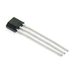
DRV5053
SLIS153D – MAY 2014 – REVISED FEBRUARY 2023
DRV5053 Analog-Bipolar Hall Effect Sensor
1 Features
3 Description
•
•
The DRV5053 device is a chopper-stabilized Hall IC
that offers a magnetic sensing solution with superior
sensitivity stability over temperature and integrated
protection features.
•
•
•
•
•
•
•
•
Linear output hall sensor
Superior temperature stability
– Sensitivity ±10% over temperature
High sensitivity options:
– –11 mV/mT (OA, see Figure 17)
– –23 mV/mT (PA)
– –45 mV/mT (RA)
– –90 mV/mT (VA)
– +23 mV/mT (CA)
– +45 mV/mT (EA)
Supports a wide voltage range
– 2.5 V to 38 V
– No external regulator required
Wide operating temperature range
– TA = –40 to 125°C (Q, see Figure 17)
Amplified output stage
– 2.3-mA sink, 300-µA source
Output voltage: 0.2 V to approximately 1.8 V
– B = 0 mT, OUT = 1 V
Fast power-on: 35 µs
Small package and footprint
– Surface mount 3-pin SOT-23 (DBZ)
• 2.92 mm × 2.37 mm
– Through-hole 3-pin TO-92 (LPG)
• 4.00 mm × 3.15 mm
Protection features:
– Reverse supply protection (up to –22 V)
– Supports up to 40-V load dump
– Output short-circuit protection
– Output current limitation
The 0-V to 2-V analog output responds linearly to the
applied magnetic flux density, and distinguishes the
polarity of magnetic field direction. A wide operating
voltage range from 2.5 V to 38 V with reverse polarity
protection up to –22 V makes the device suitable for a
wide range of industrial and consumer applications.
Internal protection functions are provided for reverse
supply conditions, load dump, and output short circuit
or overcurrent.
Package Information(1)
PART NUMBER
DRV5053
(1)
PACKAGE
BODY SIZE (NOM)
SOT-23 (3)
2.92 mm × 1.30 mm
TO-92 (3)
4.00 mm × 3.15 mm
For all available packages, see the orderable addendum at
the end of the data sheet.
2 Applications
•
•
•
•
Flow Meters
Docking Adjustment
Vibration Correction
Damper Controls
VOUT (V)
VMAX
VQ
VMIN
BMIN (N)
B (mT)
BMAX (S)
Output State
Device Packages
An IMPORTANT NOTICE at the end of this data sheet addresses availability, warranty, changes, use in safety-critical applications,
intellectual property matters and other important disclaimers. PRODUCTION DATA.
�DRV5053
www.ti.com
SLIS153D – MAY 2014 – REVISED FEBRUARY 2023
Table of Contents
1 Features............................................................................1
2 Applications..................................................................... 1
3 Description.......................................................................1
4 Revision History.............................................................. 2
5 Pin Configuration and Functions...................................3
6 Specifications.................................................................. 4
6.1 Absolute Maximum Ratings........................................ 4
6.2 ESD Ratings............................................................... 4
6.3 Recommended Operating Conditions.........................4
6.4 Thermal Information....................................................4
6.5 Electrical Characteristics.............................................5
6.6 Switching Characteristics............................................5
6.7 Magnetic Characteristics.............................................5
6.8 Typical Characteristics................................................ 7
7 Detailed Description........................................................8
7.1 Overview..................................................................... 8
7.2 Functional Block Diagram........................................... 8
7.3 Feature Description.....................................................9
7.4 Device Functional Modes..........................................11
8 Application and Implementation.................................. 12
8.1 Application Information............................................. 12
8.2 Typical Applications.................................................. 12
8.3 Power Supply Recommendations.............................14
9 Device and Documentation Support............................15
9.1 Device Support......................................................... 15
9.2 Receiving Notification of Documentation Updates....15
9.3 Support Resources................................................... 15
9.4 Trademarks............................................................... 16
9.5 Electrostatic Discharge Caution................................16
9.6 Glossary....................................................................16
10 Mechanical, Packaging, and Orderable
Information.................................................................... 16
4 Revision History
Changes from Revision C (December 2015) to Revision D (February 2023)
Page
• Updated the numbering format for tables, figures, and cross-references throughout the document .................1
• Changed the Device Information table title to Package Information ..................................................................1
• Moved the Power Supply Recommendations section to the Application and Implementation section.............14
Changes from Revision B (September 2014) to Revision C (December 2015)
Page
• Corrected body size of SOT-23 package and SIP package name to TO-92 ..................................................... 1
• Added BMAX to Absolute Maximum Ratings ...................................................................................................... 4
• Removed table note from junction temperature .................................................................................................4
• Updated the typical value for BN and VN for each version.................................................................................. 5
• Updated Figure 6-6 ............................................................................................................................................7
• Updated the Functional Block Diagram ............................................................................................................. 8
• Updated Output Stage ..................................................................................................................................... 11
• Updated package tape and reel options for M and blank ................................................................................ 15
Changes from Revision A (August 2014) to Revision B (September 2014)
Page
• Updated high sensitivity options ........................................................................................................................ 1
• Updated the sensitivity device values and typicals. Updated typical and max values for DRV5053VA: –80
mV/mT ............................................................................................................................................................... 5
• Updated Typical Characteristics graphs ............................................................................................................ 7
Changes from Revision * (May 2014) to Revision A (August 2014)
Page
• Updated device status to production data ......................................................................................................... 1
• Changed the maximum TJ value from 175°C to 150°C ..................................................................................... 4
• Updated Magnetic Characteristics table. ........................................................................................................... 5
2
Submit Document Feedback
Copyright © 2023 Texas Instruments Incorporated
Product Folder Links: DRV5053
�DRV5053
www.ti.com
SLIS153D – MAY 2014 – REVISED FEBRUARY 2023
5 Pin Configuration and Functions
For additional configuration information, see Device Markings and Mechanical, Packaging, and Orderable
Information.
OUT
2
GND
3
1
1
2
3
VCC
Figure 5-1. DBZ Package 3-Pin SOT-23 Top View
VCC
OUT
GND
Figure 5-2. LPG Package 3-Pin TO-92 Top View
Table 5-1. Pin Functions
PIN
NAME
TYPE
DESCRIPTION
DBZ
LPG
GND
3
2
GND
VCC
1
1
Power
2.5 V to 38 V power supply. Bypass this pin to the GND pin with a 0.01-μF (minimum)
ceramic capacitor rated for VCC.
OUT
2
3
Output
Hall sensor analog output. 1 V output corresponds to B = 0 mT
Ground pin
Submit Document Feedback
Copyright © 2023 Texas Instruments Incorporated
Product Folder Links: DRV5053
3
�DRV5053
www.ti.com
SLIS153D – MAY 2014 – REVISED FEBRUARY 2023
6 Specifications
6.1 Absolute Maximum Ratings
over operating free-air temperature range (unless otherwise noted)(1)
VCC
MIN
MAX
UNIT
–22(2)
40
V
Voltage ramp rate (VCC), VCC < 5 V
Power supply voltage
Unlimited
Voltage ramp rate (VCC), VCC > 5 V
0
Output pin voltage
Output pin reverse current during reverse supply condition
V/µs
2
–0.5
2.5
V
0
–20
mA
Magnetic flux density, BMAX
Unlimited
Operating junction temperature, TJ
–40
150
°C
Storage temperature, Tstg
–65
150
°C
(1)
(2)
Operation outside the Absolute Maximum Ratings may cause permanent device damage. Absolute Maximum Ratings do not imply
functional operation of the device at these or any other conditions beyond those listed under Recommended Operating Conditions.
If used outside the Recommended Operating Conditions but within the Absolute Maximum Ratings, the device may not be fully
functional, and this may affect device reliability, functionality, performance, and shorten the device lifetime.
Specified by design. Only tested to –20 V.
6.2 ESD Ratings
VALUE
V(ESD)
(1)
(2)
Electrostatic
discharge
Human body model (HBM), per ANSI/ESDA/JEDEC JS-001, all pins(1)
±2500
Charged device model (CDM), per ANSI/ESDA/JEDEC JS-002, all pins(2)
±500
UNIT
V
JEDEC document JEP155 states that 500-V HBM allows safe manufacturing with a standard ESD control process.
JEDEC document JEP157 states that 250-V CDM allows safe manufacturing with a standard ESD control process.
6.3 Recommended Operating Conditions
over operating free-air temperature range (unless otherwise noted)
MIN
MAX
UNIT
VCC
Power supply voltage
2.5
38
V
VOUT
Output pin voltage (OUT)
0
2
V
ISOURCE
Output pin current source (OUT)
0
300
µA
ISINK
Output pin current sink (OUT)
0
2.3
mA
TA
Operating ambient temperature
–40
125
°C
6.4 Thermal Information
DRV5053
THERMAL METRIC(1)
LPG (TO-92)
UNIT
3 PINS
3 PINS
RθJA
Junction-to-ambient thermal resistance
333.2
180
°C/W
RθJC(top)
Junction-to-case (top) thermal resistance
99.9
98.6
°C/W
RθJB
Junction-to-board thermal resistance
66.9
154.9
°C/W
ψJT
Junction-to-top characterization parameter
4.9
40
°C/W
ψJB
Junction-to-board characterization parameter
65.2
154.9
°C/W
(1)
4
DBZ (SOT-23)
For more information about traditional and new thermal metrics, see the Semiconductor and IC Package Thermal Metrics application
report, SPRA953.
Submit Document Feedback
Copyright © 2023 Texas Instruments Incorporated
Product Folder Links: DRV5053
�DRV5053
www.ti.com
SLIS153D – MAY 2014 – REVISED FEBRUARY 2023
6.5 Electrical Characteristics
over operating free-air temperature range (unless otherwise noted)
PARAMETER
TEST CONDITIONS
MIN
TYP
MAX
UNIT
POWER SUPPLIES (VCC)
VCC
VCC operating voltage
ICC
Operating supply current
ton
Power-on time
2.5
VCC = 2.5 V to 38 V, TA = 25°C
38
2.7
VCC = 2.5 V to 38 V, TA = 125°C
3
3.6
35
50
V
mA
µs
PROTECTION CIRCUITS
VCCR
Reverse supply voltage
IOCP,SOURCE
Overcurrent protection level
Sourcing current
–22
300
µA
V
IOCP,SINK
Overcurrent protection level
Sinking current
2.3
mA
6.6 Switching Characteristics
over operating free-air temperature range (unless otherwise noted)
PARAMETER
TEST CONDITIONS
MIN
TYP
MAX
13
25
UNIT
ANALOG OUTPUT (OUT)
td
Output delay time
TA = 25°C
µs
6.7 Magnetic Characteristics
over operating free-air temperature range (unless otherwise noted)
PARAMETER
VQ
Quiescent output
ƒBW
Bandwidth(3)
TEST CONDITIONS
B = 0 mT
TA = –40°C to 125°C
MIN
TYP
MAX
UNIT(2)
0.9
1.02
1.15
V
20
BN
Input-referred noise(1)
COUT = 50 pF
TA = –40°C to 125°C
Le
Linearity(4)
–BSAT < B < BSAT
VOUT MIN
Output saturation voltage (minimum) B < –BSAT
VOUT MAX
Output saturation voltage (maximum) B > BSAT
0.40
kHz
0.49
0.79
mTpp
0.2
V
1%
1.8
V
DRV5053OA: –11 mV/mT
S
Sensitivity
VCC = 3.3 V
TA ≈ –40°C to 125°C
VN
Output-referred noise
VCC = 3.3 V; ROUT = 10 kΩ;
COUT = 50 pF
TA ≈ –40°C to 125°C
BSAT
Input saturation field
VCC = 3.3 V
TA ≈ –40°C to 125°C
–17.5
–11
–5
mV/mT
5
mVpp
73
mT
DRV5053PA: –23 mV/mT
S
Sensitivity
VCC = 3.3 V
TA ≈ –40°C to 125°C
VN
Output-referred noise
VCC = 3.3 V; ROUT = 10 kΩ;
COUT = 50 pF
TA ≈ –40°C to 125°C
11
mVpp
BSAT
Input saturation field
VCC = 3.3 V
TA ≈ –40°C to 125°C
35
mT
–35
–23
–10
mV/mT
Submit Document Feedback
Copyright © 2023 Texas Instruments Incorporated
Product Folder Links: DRV5053
5
�DRV5053
www.ti.com
SLIS153D – MAY 2014 – REVISED FEBRUARY 2023
over operating free-air temperature range (unless otherwise noted)
PARAMETER
TEST CONDITIONS
MIN
TYP
MAX
UNIT(2)
–70
–45
–20
mV/mT
DRV5053RA: –45 mV/mT
S
Sensitivity
VCC = 3.3 V
TA ≈ –40°C to 125°C
VN
Output-referred noise
VCC = 3.3 V; ROUT = 10 kΩ;
COUT = 50 pF
TA ≈ –40°C to 125°C
22
mVpp
BSAT
Input saturation field
VCC = 3.3 V
TA ≈ –40°C to 125°C
18
mT
DRV5053VA: –90 mV/mT
S
Sensitivity
VCC = 3.3 V
TA ≈ –40°C to 125°C
VN
Output-referred noise
VCC = 3.3 V; ROUT = 10 kΩ;
COUT = 50 pF
TA ≈ –40°C to 125°C
BSAT
Input saturation field
VCC = 3.3 V
TA ≈ –40°C to 125°C
–140
–90
–45
mV/mT
44
mVpp
9
mT
DRV5053CA: 23 mV/mT
S
Sensitivity
VCC = 3.3 V
TA ≈ –40°C to 125°C
VN
Output-referred noise
VCC = 3.3 V; ROUT = 10 kΩ;
COUT = 50 pF
TA ≈ –40°C to 125°C
11
mVpp
BSAT
Input saturation field
VCC = 3.3 V
TA ≈ –40°C to 125°C
35
mT
10
23
35
mV/mT
DRV5053EA: 45 mV/mT
S
Sensitivity
VCC = 3.3 V
TA ≈ –40°C to 125°C
VN
Output-referred noise
VCC = 3.3 V; ROUT = 10 kΩ;
COUT = 50 pF
TA ≈ –40°C to 125°C
22
mVpp
BSAT
Input saturation field
VCC = 3.3 V
TA ≈ –40°C to 125°C
18
mT
(1)
(2)
(3)
(4)
6
20
45
70
mV/mT
Not tested in production; limits are based on characterization data.
1 mT = 10 Gauss
Bandwidth describes the fastest changing magnetic field that can be detected and translated to the output.
Linearity describes the change in sensitivity across the B-range. The sensitivity near BSAT is typically within 1% of the sensitivity near
B = 0 mT.
Submit Document Feedback
Copyright © 2023 Texas Instruments Incorporated
Product Folder Links: DRV5053
�DRV5053
www.ti.com
SLIS153D – MAY 2014 – REVISED FEBRUARY 2023
6.8 Typical Characteristics
3.5
TA ± ƒ&
TA = 25°C
TA = 75°C
TA = 125°C
Supply Current (mA)
Supply Current (mA)
3.5
3
2.5
2
0
10
20
Supply Voltage (V)
30
VCC = 2.5 V
VCC = 3.3 V
VCC = 13.2 V
VCC = 38 V
3
2.5
2
-50
40
-25
Figure 6-1. ICC vs VCC
60
DRV5053EA
125
150
D010
DRV5053EA
40
Magnetic Sensitivity (mV/mT)
40
M a g n e tic S e n s itivity (m V /m T )
25
50
75
100
Ambient Temperature (qC)
Figure 6-2. ICC vs Temperature
60
DRV5053CA
20
0
DRV5053OA
DRV5053PA
-20
DRV5053RA
-40
-60
-80
0
DRV5053CA
20
0 DRV5053OA
-20 DRV5053PA
-40
DRV5053RA
-60
-80
DRV5053VA
-100
DRV5053VA
-120
-50
-100
10
20
Supply Voltage (V)
30
40
1.03
0.65
Input-Referred Noise (mTpp)
0.7
1.025
1.02
1.015
1.01
TA ± ƒ&
TA = 25°C
TA = 85°C
TA = 125°C
125
D002
0.6
0.55
0.5
0.45
0.4
0.35
1
0.3
-50
0.995
10
100
Figure 6-4. Sensitivity vs Temperature
1.035
0
0
25
50
75
Ambient Temperature (°C)
VCC = 3.3 V
Figure 6-3. Sensitivity vs VCC
1.005
-25
D001
TA = 25°C
Quiescent Voltage VQ (V)
0
D009
20
Supply Voltage (V)
TA = 25°C
Figure 6-5. VQ vs VCC
30
-25
40
D003
0
25
50
75
Ambient Temperature (°C)
100
125
D004
VCC = 3.3 V
Figure 6-6. BN vs Temperature
Submit Document Feedback
Copyright © 2023 Texas Instruments Incorporated
Product Folder Links: DRV5053
7
�DRV5053
www.ti.com
SLIS153D – MAY 2014 – REVISED FEBRUARY 2023
7 Detailed Description
7.1 Overview
The DRV5053 device is a chopper-stabilized Hall sensor with an analog output for magnetic sensing
applications. The DRV5053 device can be powered with a supply voltage between 2.5 V and 38 V, and will
survive –22 V reverse battery conditions continuously. Note that the DRV5053 device will not be operating when
approximately –22 V to 2.4 V is applied to VCC (with respect to GND). In addition, the device can withstand
supply voltages up to 40 V for transient durations.
The output voltage is dependent on the magnetic field perpendicular to the package. The absence of a magnetic
field will result in OUT = 1 V. A magnetic field will cause the output voltage to change linearly with the magnetic
field.
The field polarity is defined as follows: a south pole near the marked side of the package is a positive magnetic
field. A north pole near the marked side of the package is a negative magnetic field.
For devices with a negative sensitivity (that is, DRV5053RA: –40 mV/mT), a south pole will cause the output
voltage to drop below 1 V, and a north pole will cause the output to rise above 1 V.
For devices with a positive sensitivity (that is, DRV5053EA: +40 mV/mT), a south pole will cause the output
voltage to rise above 1 V, and a north pole will cause the output to drop below 1 V.
7.2 Functional Block Diagram
2.5 ± 38 V
CVCC
VCC
Regulated Supply
Bias
Offset Cancel
Hall Element
Temperature
Compensation
+
-
OUT
Output
Driver
COUT
Optional RC Filtering
GND
8
Submit Document Feedback
ROUT
Equivalent
impedance to
ground
Copyright © 2023 Texas Instruments Incorporated
Product Folder Links: DRV5053
�DRV5053
www.ti.com
SLIS153D – MAY 2014 – REVISED FEBRUARY 2023
7.3 Feature Description
7.3.1 Field Direction Definition
Figure 7-1 shows the positive magnetic field defined as a south pole near the marked side of the package.
SOT-23 (DBZ)
TO-92 (LPG, LPE)
B > 0 mT
B < 0 mT
B > 0 mT
B < 0 mT
N
S
N
S
S
N
S
N
1
2
3
1
2
3
(Bottom view)
N = North pole, S = South pole
Figure 7-1. Field Direction Definition
7.3.2 Device Output
The DRV5053 device output is defined below for negative sensitivity (that is, –45 mV/mT, RA) and positive
sensitivity (that is, +45 mV/mT, EA):
VOUT (V)
VMAX
VQ
VMIN
–BSAT (N)
B (mT)
BSAT (S)
Figure 7-2. DRV5053 – Negative Sensitivity
VOUT (V)
VMAX
VQ
VMIN
–BSAT (N)
B (mT)
BSAT (S)
Figure 7-3. DRV5053 – Positive Sensitivity
Submit Document Feedback
Copyright © 2023 Texas Instruments Incorporated
Product Folder Links: DRV5053
9
�DRV5053
www.ti.com
SLIS153D – MAY 2014 – REVISED FEBRUARY 2023
7.3.3 Power-On Time
After applying VCC to the DRV5053 device, ton must elapse before OUT is valid. Figure 7-4 shows Case 1 and
Figure 7-5 shows Case 2. The output is defined assuming a negative sensitivity device and a constant magnetic
field –BSAT < B < BSAT.
Case #1
VCC
t (s)
B (mT)
BSAT
t (s)
-BSAT
OUT
90%
Invalid Output
Valid Output
t (s)
tON
Figure 7-4. Case 1: Power On When B < 0, North
Case #2
VCC
t (s)
B (mT)
BSAT
t (s)
-BSAT
OUT
Invalid Output
Valid Output
10%
t (s)
tON
Figure 7-5. Case 2: Power On When B > 0, South
10
Submit Document Feedback
Copyright © 2023 Texas Instruments Incorporated
Product Folder Links: DRV5053
�DRV5053
www.ti.com
SLIS153D – MAY 2014 – REVISED FEBRUARY 2023
7.3.4 Output Stage
The DRV5053 output stage is capable of up to 300-μA of current source or 2.3-mA sink. For proper operation,
ensure that equivalent output load ROUT > 10 kΩ.
The capacitive load directly present on the OUT pin should be less than 10 nF to ensure the internal operational
amplifier is stable. If an external RC filter is added to reduce noise, it is acceptable to use a resistor ≥ 200 Ω with
a capacitor ≤ 0.1 µF. For an application example, see Filtered Typical Application.
7.3.5 Protection Circuits
An analog current limit circuit limits the current through the output driver. The driver current will be clamped to
IOCP.
7.3.5.1 Overcurrent Protection (OCP)
An analog current-limit circuit limits the current through the FET. The driver current is clamped to IOCP. During
this clamping, the rDS(on) of the output FET is increased from the nominal value.
7.3.5.2 Load Dump Protection
The DRV5053 device operates at DC VCC conditions up to 38 V nominally, and can additionally withstand VCC =
40 V. No current-limiting series resistor is required for this protection.
7.3.5.3 Reverse Supply Protection
The DRV5053 device is protected in the event that the VCC pin and the GND pin are reversed (up to –22 V).
Note
In a reverse supply condition, the OUT pin reverse-current must not exceed the ratings specified in the
Absolute Maximum Ratings.
FAULT
CONDITION
DEVICE
DESCRIPTION
RECOVERY
FET overload (OCP)
ISINK ≥ IOCP
Operating
Output current is clamped to IOCP
IO < IOCP
Load Dump
38 V < VCC < 40 V
Operating
Device will operate for a transient duration
VCC ≤ 38 V
Reverse Supply
–22 V < VCC < 0 V
Disabled
Device will survive this condition
VCC ≥ 2.5 V
7.4 Device Functional Modes
The DRV5053 device is active only when VCC is between 2.5 V and 38 V.
When a reverse supply condition exists, the device is inactive.
Submit Document Feedback
Copyright © 2023 Texas Instruments Incorporated
Product Folder Links: DRV5053
11
�DRV5053
www.ti.com
SLIS153D – MAY 2014 – REVISED FEBRUARY 2023
8 Application and Implementation
Note
Information in the following applications sections is not part of the TI component specification,
and TI does not warrant its accuracy or completeness. TI’s customers are responsible for
determining suitability of components for their purposes, as well as validating and testing their design
implementation to confirm system functionality.
8.1 Application Information
The DRV5053 device is used in magnetic-field sensing applications.
8.2 Typical Applications
8.2.1 Typical Application With No Filter
2
OUT
3
VCC
1
VCC
C1
0.01 µF
(minimum)
Figure 8-1. Typical Application Schematic – No Filter
8.2.1.1 Design Requirements
For this design example, use the parameters listed in Table 8-1 as the input parameters.
Table 8-1. Design Parameters
DESIGN PARAMETER
REFERENCE
EXAMPLE VALUE
System bandwidth
ƒBW
15 kHz
8.2.1.2 Detailed Design Procedure
The DRV5053 has internal filtering that limits the bandwidth to at least 20 kHz. For this application no external
components are required other than the C1 bypass capacitor, which is 0.01 µF minimum. If the analog output
OUT is tied to a microcontroller ADC input, the equivalent load must be R > 10 kΩ and C < 10 nF.
Table 8-2. External Components
COMPONENT
PIN 1
PIN 2
RECOMMENDED
C1
VCC
GND
A 0.01-µF (minimum) ceramic capacitor rated for VCC
12
Submit Document Feedback
Copyright © 2023 Texas Instruments Incorporated
Product Folder Links: DRV5053
�DRV5053
www.ti.com
SLIS153D – MAY 2014 – REVISED FEBRUARY 2023
8.2.1.3 Application Curve
Figure 8-2. 10-kHz Switching Magnetic Field
8.2.2 Filtered Typical Application
For lower noise on the analog output OUT, additional RC filtering can be added to further reduce the bandwidth.
C2
1500 pF
2
OUT
R1
10 kΩ
3
1
VCC
VCC
C1
0.01 µF
(minimum)
Figure 8-3. Filtered Typical Application Schematic
8.2.2.1 Design Requirements
For this design example, use the parameters listed in Table 8-3 as the input parameters.
Table 8-3. Design Parameters
DESIGN PARAMETER
REFERENCE
EXAMPLE VALUE
System bandwidth
ƒBW
5 kHz
Submit Document Feedback
Copyright © 2023 Texas Instruments Incorporated
Product Folder Links: DRV5053
13
�DRV5053
www.ti.com
SLIS153D – MAY 2014 – REVISED FEBRUARY 2023
8.2.2.2 Detailed Design Procedure
In this example we will add an external RC filter in order to reduce the output bandwidth.
In order to preserve the signal at the frequencies of interest, we will conservatively select a low-pass filter
bandwidth (–3-dB point) at twice the system bandwidth (10 kHz).
10 kHz
1
2p ´ R1 ´ C2
(1)
If we guess R1 = 10 kΩ, then C2 < 1590 pF. So we select C2 = 1500 pF.
8.2.2.2.1 Typical Noise Versus Cutoff Frequency
RC filters are an effective way to reduce the noise present on OUT. The following shows typical noise
measurements for different cutoff frequencies using the DRV5053VA.
Table 8-4. DRV5053VA Typical Noise Data
R (Ω)
C (µF)
fCUTOFF (kHz)
NOISE (mVpp)
163
0.1
9.8
30.4
349
0.1
4.6
22.8
750
0.1
2.1
15.2
1505
0.1
1.1
9.7
3322
0.1
0.5
5.3
7510
0.1
0.2
2.5
8.2.2.3 Application Curves
0
-2
Magnitude (dB)
-4
-6
-8
-10
-12
.
.
.
.
-14
100
200
500 1000 2000
5000 10000
Frequency (Hz)
R1 = 10-kΩ pullup
Figure 8-4. 5-kHz Switching Magnetic Field
100000
D011
C2 = 680 pF
Figure 8-5. Low-Pass Filtering
8.3 Power Supply Recommendations
The DRV5053 device is designed to operate from an input voltage supply (VM) range between 2.5 V and 38 V. A
0.01-µF (minimum) ceramic capacitor rated for VCC must be placed as close to the DRV5053 device as possible.
14
Submit Document Feedback
Copyright © 2023 Texas Instruments Incorporated
Product Folder Links: DRV5053
�DRV5053
www.ti.com
SLIS153D – MAY 2014 – REVISED FEBRUARY 2023
9 Device and Documentation Support
9.1 Device Support
9.1.1 Device Nomenclature
Figure 9-1 shows a legend for reading the complete device name for the DRV5053 device.
DRV5053
(RA)
(Q)
(DBZ)
(R)
()
Prefix
DRV5053: Analog linear Hall sensor
AEC-Q100
Q1: Automotive qualification
Blank: Non-auto
Sensitivity
OA: ±11 mV/mT
PA: ±23 mV/mT
RA: ±45 mV/mT
VA: ±90 mV/mT
CA: +23 mV/mT
EA: +45 mV/mT
Tape and Reel
R: 3000 pcs/reel
T: 250 pcs/reel
M: 3000 pcs/box (ammo)
Blank: 1000 pcs/bag (bulk)
Package
DBZ: 3-pin SOT-23
LPG: 3-pin TO-92
Temperature Range
Q: ±40 to 125°C
E: ±40 to 150°C
Figure 9-1. Device Nomenclature
9.1.2 Device Markings
Marked Side Front
Marked Side
3
1
1
2
3
2
Marked Side
1
2
3
(Bottom view)
Figure 9-2. SOT-23 (DBZ) Package
Figure 9-3. TO-92 (LPG) Package
9.2 Receiving Notification of Documentation Updates
To receive notification of documentation updates, navigate to the device product folder on ti.com. Click on
Subscribe to updates to register and receive a weekly digest of any product information that has changed. For
change details, review the revision history included in any revised document.
9.3 Support Resources
TI E2E™ support forums are an engineer's go-to source for fast, verified answers and design help — straight
from the experts. Search existing answers or ask your own question to get the quick design help you need.
Submit Document Feedback
Copyright © 2023 Texas Instruments Incorporated
Product Folder Links: DRV5053
15
�DRV5053
www.ti.com
SLIS153D – MAY 2014 – REVISED FEBRUARY 2023
Linked content is provided "AS IS" by the respective contributors. They do not constitute TI specifications and do
not necessarily reflect TI's views; see TI's Terms of Use.
9.4 Trademarks
TI E2E™ is a trademark of Texas Instruments.
All trademarks are the property of their respective owners.
9.5 Electrostatic Discharge Caution
This integrated circuit can be damaged by ESD. Texas Instruments recommends that all integrated circuits be handled
with appropriate precautions. Failure to observe proper handling and installation procedures can cause damage.
ESD damage can range from subtle performance degradation to complete device failure. Precision integrated circuits may
be more susceptible to damage because very small parametric changes could cause the device not to meet its published
specifications.
9.6 Glossary
TI Glossary
This glossary lists and explains terms, acronyms, and definitions.
10 Mechanical, Packaging, and Orderable Information
The following pages include mechanical, packaging, and orderable information. This information is the most
current data available for the designated devices. This data is subject to change without notice and revision of
this document. For browser-based versions of this data sheet, refer to the left-hand navigation.
16
Submit Document Feedback
Copyright © 2023 Texas Instruments Incorporated
Product Folder Links: DRV5053
�PACKAGE OPTION ADDENDUM
www.ti.com
26-Jan-2023
PACKAGING INFORMATION
Orderable Device
Status
(1)
Package Type Package Pins Package
Drawing
Qty
Eco Plan
(2)
Lead finish/
Ball material
MSL Peak Temp
Op Temp (°C)
Device Marking
(3)
Samples
(4/5)
(6)
DRV5053CAQDBZR
ACTIVE
SOT-23
DBZ
3
3000
RoHS & Green
NIPDAUAG | SN
Level-1-260C-UNLIM
-40 to 125
(+ALCA, 1LX2)
Samples
DRV5053CAQDBZT
ACTIVE
SOT-23
DBZ
3
250
RoHS & Green
NIPDAUAG | SN
Level-1-260C-UNLIM
-40 to 125
(+ALCA, 1LX2)
Samples
DRV5053CAQLPG
ACTIVE
TO-92
LPG
3
1000
RoHS & Green
SN
N / A for Pkg Type
-40 to 125
+ALCA
Samples
DRV5053CAQLPGM
ACTIVE
TO-92
LPG
3
3000
RoHS & Green
SN
N / A for Pkg Type
-40 to 125
+ALCA
Samples
DRV5053EAQDBZR
ACTIVE
SOT-23
DBZ
3
3000
RoHS & Green
NIPDAUAG | SN
Level-1-260C-UNLIM
-40 to 125
(+ALEA, 1LZ2)
Samples
DRV5053EAQDBZT
ACTIVE
SOT-23
DBZ
3
250
RoHS & Green
NIPDAUAG | SN
Level-1-260C-UNLIM
-40 to 125
(+ALEA, 1LZ2)
Samples
DRV5053EAQLPG
ACTIVE
TO-92
LPG
3
1000
RoHS & Green
SN
N / A for Pkg Type
-40 to 125
+ALEA
Samples
DRV5053EAQLPGM
ACTIVE
TO-92
LPG
3
3000
RoHS & Green
SN
N / A for Pkg Type
-40 to 125
+ALEA
Samples
DRV5053OAQDBZR
ACTIVE
SOT-23
DBZ
3
3000
RoHS & Green
NIPDAUAG | SN
Level-1-260C-UNLIM
-40 to 125
(+ALOA, 1M12)
Samples
DRV5053OAQDBZT
ACTIVE
SOT-23
DBZ
3
250
RoHS & Green
NIPDAUAG | SN
Level-1-260C-UNLIM
-40 to 125
(+ALOA, 1M12)
Samples
DRV5053OAQLPG
ACTIVE
TO-92
LPG
3
1000
RoHS & Green
SN
N / A for Pkg Type
-40 to 125
+ALOA
Samples
DRV5053OAQLPGM
ACTIVE
TO-92
LPG
3
3000
RoHS & Green
SN
N / A for Pkg Type
-40 to 125
+ALOA
Samples
DRV5053PAQDBZR
ACTIVE
SOT-23
DBZ
3
3000
RoHS & Green
NIPDAUAG | SN
Level-1-260C-UNLIM
-40 to 125
(+ALPA, 1M22)
Samples
DRV5053PAQDBZT
ACTIVE
SOT-23
DBZ
3
250
RoHS & Green
NIPDAUAG | SN
Level-1-260C-UNLIM
-40 to 125
(+ALPA, 1M22)
Samples
DRV5053PAQLPG
ACTIVE
TO-92
LPG
3
1000
RoHS & Green
SN
N / A for Pkg Type
-40 to 125
+ALPA
Samples
DRV5053PAQLPGM
ACTIVE
TO-92
LPG
3
3000
RoHS & Green
SN
N / A for Pkg Type
-40 to 125
+ALPA
Samples
DRV5053RAQDBZR
ACTIVE
SOT-23
DBZ
3
3000
RoHS & Green
NIPDAUAG | SN
Level-1-260C-UNLIM
-40 to 125
(+ALRA, 1M32)
Samples
DRV5053RAQDBZT
ACTIVE
SOT-23
DBZ
3
250
RoHS & Green
NIPDAUAG | SN
Level-1-260C-UNLIM
-40 to 125
(+ALRA, 1M32)
Samples
DRV5053RAQLPG
ACTIVE
TO-92
LPG
3
1000
RoHS & Green
SN
N / A for Pkg Type
-40 to 125
+ALRA
Samples
DRV5053RAQLPGM
ACTIVE
TO-92
LPG
3
3000
RoHS & Green
SN
N / A for Pkg Type
-40 to 125
+ALRA
Samples
Addendum-Page 1
�PACKAGE OPTION ADDENDUM
www.ti.com
Orderable Device
26-Jan-2023
Status
(1)
Package Type Package Pins Package
Drawing
Qty
Eco Plan
(2)
Lead finish/
Ball material
MSL Peak Temp
Op Temp (°C)
Device Marking
(3)
Samples
(4/5)
(6)
DRV5053VAQDBZR
ACTIVE
SOT-23
DBZ
3
3000
RoHS & Green
NIPDAUAG | SN
Level-1-260C-UNLIM
-40 to 125
(+ALVA, 1M42)
Samples
DRV5053VAQDBZT
ACTIVE
SOT-23
DBZ
3
250
RoHS & Green
NIPDAUAG | SN
Level-1-260C-UNLIM
-40 to 125
(+ALVA, 1M42)
Samples
DRV5053VAQLPG
ACTIVE
TO-92
LPG
3
1000
RoHS & Green
SN
N / A for Pkg Type
-40 to 125
+ALVA
Samples
DRV5053VAQLPGM
ACTIVE
TO-92
LPG
3
3000
RoHS & Green
SN
N / A for Pkg Type
-40 to 125
+ALVA
Samples
(1)
The marketing status values are defined as follows:
ACTIVE: Product device recommended for new designs.
LIFEBUY: TI has announced that the device will be discontinued, and a lifetime-buy period is in effect.
NRND: Not recommended for new designs. Device is in production to support existing customers, but TI does not recommend using this part in a new design.
PREVIEW: Device has been announced but is not in production. Samples may or may not be available.
OBSOLETE: TI has discontinued the production of the device.
(2)
RoHS: TI defines "RoHS" to mean semiconductor products that are compliant with the current EU RoHS requirements for all 10 RoHS substances, including the requirement that RoHS substance
do not exceed 0.1% by weight in homogeneous materials. Where designed to be soldered at high temperatures, "RoHS" products are suitable for use in specified lead-free processes. TI may
reference these types of products as "Pb-Free".
RoHS Exempt: TI defines "RoHS Exempt" to mean products that contain lead but are compliant with EU RoHS pursuant to a specific EU RoHS exemption.
Green: TI defines "Green" to mean the content of Chlorine (Cl) and Bromine (Br) based flame retardants meet JS709B low halogen requirements of