User's Guide
SBOU078 – June 2009
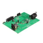
PGA2505EVM
This document provides the information needed to set up and operate the PGA2505EVM evaluation
module (EVM) and accompanying software. For a detailed description of the PGA2505 device, please
refer to the product data sheet available from the Texas Instruments web site at www.ti.com. Additional
support documents are listed in the section of this guide entitled Related Documentation from Texas
Instruments.
1
2
3
4
5
6
Contents
Preface ........................................................................................................................ 2
Introduction ................................................................................................................... 3
Getting Started ............................................................................................................... 6
Setup Guide .................................................................................................................. 7
Software Installation and Operation ..................................................................................... 10
Schematic, PCB Layout, and Bill of Materials .......................................................................... 15
List of Figures
1
2
3
4
5
6
7
8
9
10
11
12
13
14
15
16
PGA2505 Functional Block Diagram ...................................................................................... 3
PGA2505 Serial Port Protocol ............................................................................................. 4
Functional Block Diagram for the PGA2505EVM........................................................................ 6
Recommended Power-Supply Connections.............................................................................. 7
Microphone Input Connector Configuration .............................................................................. 8
Preamp Output Connector Configuration ................................................................................. 9
PGA2505EVM Software Setup Screen.................................................................................. 11
PGA2505EVM Software Installation Directory Screen ................................................................ 11
PGA2505EVM Software Program Group Selection Panel ............................................................ 12
File Version Conflict Dialog Window ..................................................................................... 12
PGA2505EVM Software Setup Completion ............................................................................ 13
Applications Software Device Panel ..................................................................................... 13
Schematic ................................................................................................................... 15
PGA2505EVM PCB Silkscreen ........................................................................................... 16
PGA2505EVM PCB Top Layer (Component Side) .................................................................... 17
PGA2505EVM PCB Bottom Layer (Solder Side) ...................................................................... 18
List of Tables
1
2
3
Absolute Maximum Operating Conditions ................................................................................ 7
Jumper Configuration Quick Reference ................................................................................. 10
PGA2505EVM Bill of Materials ........................................................................................... 19
Microsoft, Windows are registered trademarks of Microsoft Corporation.
All other trademarks are the property of their respective owners.
SBOU078 – June 2009
Submit Documentation Feedback
PGA2505EVM
1
�Preface
www.ti.com
1
Preface
1.1
How to Use This Manual
Throughout this document, the abbreviation EVM and the term evaluation module are synonymous with
the PGA2505EVM.
Section 2 provides an overview for the PGA2505 digitally-controlled microphone preamplifier. The
PGA2505EVM block diagram and primary features are also discussed.
Section 3 provides general information regarding EVM handling and unpacking, as well as the absolute
operating conditions for the EVM.
Section 4 provides descriptions of the primary hardware functions, as well as hardware configuration
details for the EVM.
Section 5 provides the information required to install and operate the PGA2505EVM applications software
using a personal computer running the Microsoft® Windows® 9x, 2000, or XP operating systems.
Section 6 includes the EVM electrical schematic, printed circuit board (PCB) layout, and the bill of
materials.
1.2
Related Documentation From Texas Instruments
The following documents provide information regarding Texas Instruments integrated circuits used in the
assembly of the PGA2505EVM. These documents are available from the TI web site. The last character of
the literature number corresponds to the document revision, which is current at the time of the writing of
this User’s Guide. Newer revisions may be available from the TI web site at http://www.ti.com/ or call the
Texas Instruments Literature Response Center at (800) 477–8924 or the Product Information Center at
(972) 644–5580. When ordering, identify the document(s) by both title and literature number.
1.3
Document
Literature Number
PGA2505 Product Data Sheet
SBOS396
SN74AHCT541 Product Data Sheet
SCLS269O
Information About Cautions and Warnings
This book contains caution statements. The information in a caution is provided for your protection. Please
read each caution carefully.
CAUTION
This is an example of a caution statement. A caution statement describes a
situation that could potentially damage your software or equipment.
1.4
If You Need Assistance
If you have questions either regarding the use of this evaluation module or the information contained in the
accompanying documentation, please contact the Texas Instruments Product Information Center at (972)
644–5580 or visit the TI Semiconductor Online Technical Support pages at www.ti.com.
2
PGA2505EVM
SBOU078 – June 2009
Submit Documentation Feedback
�Introduction
www.ti.com
1.5
FCC Warning
This equipment is intended for use in a laboratory test environment only. It may generate, use, or radiate
radio frequency energy and has not been tested for compliance with the limits of computing devices
pursuant to subpart J of part 15 of the FCC regulations, which are designed to provide reasonable
protection against radio frequency interference. Operation of this equipment in other environments may
cause interference with radio communications, in which case the user at his own expense will be required
to take whatever measures may be required to correct this interference.
2
Introduction
This chapter provides a brief technical overview for the PGA2505 digitally-controlled microphone
preamplifier, as well as a general description and feature list for the PGA2505EVM.
2.1
PGA2505 Product Overview
The PGA2505 is a digitally-controlled, microphone preamplifier integrated circuit designed for amplifying
the output of dynamic and condenser microphones and driving high-performance audio analog-to-digital
(A/D) converters. A functional block diagram of the PGA2505 is shown in Figure 1.
GPO1
CS
GPO2
SCLK
SERIAL
PORT and
LOGIC
CONTROL
GPO3
GPO4
SDI
SDO
OVR
VCOMIN
VOUT+
VIN+
PGA
VOUT-
VIN(1)
Gain Range
AGND
VA+
VA-
(2)
CS1
DGND
DC
Servo
VD-
CS2
(1)
Gain Range: 0dB, or +9dB to +60dB (3dB/step).
(2)
CS1 and CS2 are external dc servo integrator capacitors, and are connected across the CS11/CS12 and
CS21/CS22 pins, respectively.
Figure 1. PGA2505 Functional Block Diagram
The analog input to the preamplifier is provided differentially at the VIN+ and VIN– inputs (pins 24 and 23,
respectively). The programmable gain amplifier can be programmed to either unity gain, or adjustable over
the full 9dB to 60dB range in 3dB steps. The differential output of the PGA2505 is made available at
VOUT+ and VOUT– (pins 15 and 14, respectively). Gain is controlled using a serial port interface (SPI).
SBOU078 – June 2009
Submit Documentation Feedback
PGA2505EVM
3
�Introduction
www.ti.com
The four-wire serial port interface is used to program the PGA2505 gain and support functions. A 16-bit
control word is used to program these functions, as Figure 2 illustrates. A serial data output pin provides
support for daisy-chaining multiple PGA2505 devices on a single serial interface bus.
CS
SCLK
SDI
Data Ignored
DC
CM
ZC
OR
D4
D3
D2
D1
0
0
G5
G4
G3
G2
G1
G0
Data Ignored
SDO
High Impedance
DC
CM
ZC
OR
D4
D3
D2
D1
0
0
G5
G4
G3
G2
G1
G0
High Impedance
DC Servo Enable
(Active Low)
CM Servo Enable
(Active High)
Zero Crossing Detect
(Active High)
Over-Range Indicator Bit
(0 = 5.1VRMS, 1 = 4.0VRMS)
Data for GPO4
Preamplifier Gain
where N = G[5:0]DEC
For N = 0
Gain = 0dB
For N = 1 to 17
Gain (dB) = 6 + 3N
For N = 18 to 31
Gain = 60dB
Data for GPO3
Data for GPO2
Data for GPO1
Figure 2. PGA2505 Serial Port Protocol
The differential analog output of the PGA2505 is constantly monitored by a dc servo amplifier loop. When
enabled, the purpose of the servo loop is to minimize the dc offset voltage present at the analog outputs
by feeding back an error signal to the input stage of the programmable gain amplifier. The error signal is
then used to correct the offset. The DC servo may be disabled by setting the DC bit in the serial control
word to '1', as shown in Figure 2.
Two external capacitors are required for the dc servo loop to function properly, with one capacitor
connected between CS11 and CS12 (pins 21 and 20), and the second capacitor connected between CS21
and CS22 (pins 19 and 18). Capacitor values up to 4.7µF are recommended. However, larger valued
capacitors can be used, but will result in longer settling times for the dc servo loop. A value of 1µF is
sufficient for use in most microphone preamplifier applications.
The PGA2505 also includes a common-mode servo function. This function can be enabled and disabled
using the CM bit in the serial control word. When enabled, the CM servo provides common-mode negative
feedback at the input differential pair, resulting in very low common-mode input impedance. Note that the
differential input impedance is not affected by this feedback. This function is useful when the source is
floating, or has a high common-mode output impedance, such as with a decoupling capacitor. In this case,
the only connection between the source and the ground will be through the PGA2505 preamplifier input
resistance.
With CM enabled, input common-mode parasitic current is determined by high output impedance of the
source, not by input impedance of the amplifier. Therefore, input common-mode interference can be
reduced by lowering the common-mode input impedance without increasing the input common-mode
current. Increasing common-mode current degrades common-mode rejection. Using the common-mode
servo loop, overall common-mode rejection (or CMRR) can be improved by suppressing low and medium
frequency common-mode interference.
The common-mode servo function is designed to operate with a total common-mode input capacitance
(including the microphone cable capacitance) of up to 10nF. Beyond this limit, stable servo operation is
not ensured.
The common-mode voltage control input, named VCOMIN (pin 22), allows the PGA2505 output and input to
be dc-biased to a common-mode voltage between 0V and +2.5V. This architecture allows for a dc-coupled
interface between the PGA2505 preamplifier output and the inputs of common single-supply audio
analog-to-digital (A/D) converters.
4
PGA2505EVM
SBOU078 – June 2009
Submit Documentation Feedback
�www.ti.com
Introduction
The zero-crossing control bit, ZC in the serial control word, is provided for enabling and disabling the
internal zero-crossing detector function. Setting the ZC bitt high enables the function. Zero-crossing
detection is used to ensure gain changes on zero crossings of the analog input signal. This limits the glitch
energy associated with the switched gain network, thereby minimizing audible artifacts at the preamplifier
output. Because zero-crossing detection can add some delay when performing gain changes (up to 16ms
maximum for a detector timeout event), there may be some cases where the user may wish to disable this
function. Forcing the ZC bit low disables zero-crossing detection, and gain changes will occur immediately
when programmed.
A timeout function is implemented when ZC is held low, ensuring a maximum timeout detection limit of
16ms.
An over-range indicator output, OVR, is provided at pin 6. The over-range output is forced high when the
preamplifier output voltage exceeds one of two preset thresholds. The threshold is programmed through
the serial port interface using the OR bit. If OR = '0', then the threshold is set to 5.1VRMS differential, which
is approximately 1dB below the specified output voltage range. If OR = '1', then the threshold is set to
4.0VRMS differential, which is approximately 3dB below the maximum specified output voltage range.
The PGA2505 includes four general-purpose programmable digital outputs, named GPO1 through GPO4
(pins 2 through 5, respectively), which are controlled via the serial port interface. All four pins are
CMOS-logic-level outputs. These pins may be used to control relay drivers or switches used for external
preamplifier functions, including input pads, filtering, polarity reversal, or phantom power.
2.2
PGA2505EVM Features
The PGA2505EVM provides a convenient platform for evaluating the performance and features of the
PGA2505 device. Key EVM features include the following:
• Accepts either XLR- or TRS-balanced input connections
• Configurable front-end circuit options for prototyping pads and filters
• XLR-balanced output with flexible output loading options
• Buffered PC parallel and DATA_IN ports provide host interface connections
• DATA_OUT port allows daisy-chaining of multiple PGA2505EVM boards
• Register readback function supports host interface diagnostic capability
• LED indicators for GPOs and the over-range output (OVR)
• Common-mode voltage input (VCOMIN) terminal
• Includes applications software that is compatible with most personal computers with a built-in parallel
port and equipped with Microsoft Windows 9x, 2000, or XP operating systems
• Requires +5V and –5V analog supplies, as well as a +5V digital supply
SBOU078 – June 2009
Submit Documentation Feedback
PGA2505EVM
5
�Getting Started
2.3
www.ti.com
PGA2505EVM Block Diagram
The primary functions of the PGA2505EVM are shown in Figure 3. Configurable input and output circuitry
provide convenient prototype options, while the buffered host interface supports the supplied applications
software and alternate host configurations.
+48V
Phantom
Power
+
Microphone
Input
Preamplifier
Output
Protection Diodes
and
Configurable
Input Circuitry
PGA2505
Configurable
Output Circuitry
+
PC
Parallel Port
DB25
DATA_IN
Port
HDR
DATA_OUT
Port
HDR
Buffer
SN74AHCT541
To GPO and Over Range
Indicators and Test Points
Figure 3. Functional Block Diagram for the PGA2505EVM
3
Getting Started
This chapter provides information about handling and unpacking the PGA2505EVM, as well as the
absolute operating conditions for the board.
3.1
Electrostatic Discharge Warning
Many of the components on the PGA2505EVM are susceptible to damage by electrostatic discharge
(ESD). Customers are advised to observe proper ESD handling precautions when unpacking and handling
the EVM. Failure to observe ESD handling procedures may result in damage to the EVM components.
CAUTION
Failure to observe ESD handling procedures may result in damage to the EVM.
3.2
Unpacking the EVM
Upon opening the PGA2505EVM package, please verify that the following items are included:
• One PGA2505EVM evaluation module
• One CD-ROM, containing the applications software and support documents
• One straight-through cable, DB25 male to DB25 female, for PC parallel port interface
• One printed PGA2505EVM Evaluation Module User’s Guide (TI literature number SBOU078)
• One printed PGA2505 data sheet (TI literature number SBOS396)
If any of these items are missing, please contact the Texas Instruments Product Information Center at
(972) 644–5580 to inquire about replacements.
6
PGA2505EVM
SBOU078 – June 2009
Submit Documentation Feedback
�Setup Guide
www.ti.com
3.3
Absolute Operating Conditions Warning
CAUTION
Exceeding the absolute operating conditions may result in permanent damage
to the EVM and/or the equipment attached to it.
The user should be aware of the absolute maximum operating conditions for the evaluation module.
Table 1 summarizes the critical parameters.
Table 1. Absolute Maximum Operating Conditions
Parameter
Power-Supply Voltages
Maximum Condition
(1)
VA+
+5.5V dc
VA–
–5.5V dc
VCOM
–0.3V dc to (VA+) + 0.3V dc
VCC
+5.5V dc
Phantom Power
+50V dc
Microphone Input (J1), XLR, or TRS
(2)
Maximum Input Voltage, Differential
20.0VPP (or 7.0VRMS)
Digital Input Voltage (2)
Parallel Port (J5), DATA_IN (J6), and
DATA_OUT (J7)
(1)
(2)
4
–0.3V Minimum to +5.5V
Referenced to the GND terminal of connector J4.
Assumes VA+ = +5.0V and VA– = –5.0V.
Setup Guide
This chapter provides descriptions of the hardware components that make up the PGA2505EVM. In
addition, configuration information for power supplies, analog input and output connections, and jumpers
are provided.
4.1
Analog and Digital Power Supplies
All analog and digital power supplies are connected through terminal block J4. Figure 4 shows the
recommended power-supply connections.
VCOMIN
Power Supply
Common-Mode Voltage
Input (0V to +2.5V)
+5V Digital
Chassis (Earth) Ground
Common Ground
+5V Analog
-5V Analog
Phantom Power
Source, +48V
J2
Primary
Power Supply
J4
VCC EGND GND VCOM VA+
VA-
Figure 4. Recommended Power-Supply Connections
SBOU078 – June 2009
Submit Documentation Feedback
PGA2505EVM
7
�Setup Guide
www.ti.com
The PGA2505EVM requires two analog power supplies and one digital power supply. The analog power
supplies are VA+ and VA–, respectively. VA+ is typically set to +5.0V, while VA– is typically set to –5.0V.
The analog supplies power the PGA2505 microphone preamplifier integrated circuit. The digital power
supply, VCC, is typically set to +5.0V. The VCC supply powers the PGA2505 and the SN74AHCT541
buffer IC (U2) and the associated pull-up resistors for the digital section of the board.
An optional third analog power supply may be used for the PGA2505 common-mode dc voltage input,
VCOMIN (pin 22). The common-mode input can be connected to analog ground by shorting pins 3 and 4 of
Jumper JMP3. Alternatively, the common-mode input can be connected to the VCOM supply terminal of
connector J4 by shorting pins 1 and 2 of Jumper JMP3. The VCOM supply will typically be set to a dc
voltage within the 0V to +2.5V range (with respect to GND). The common-mode voltage biases both the
output and input terminals of the PGA2505, with the output pins being biased to the VCOMIN voltage level
and the input pins being biased to approximately (VCOMIN – 0.65V).
The GND terminal of connector J4 serves as the common ground connection for both the analog and
digital sections of the PGA2505EVM. The EGND (earth ground) terminal should be connected to the earth
or chassis ground of the power supply. The common ground (GND) and earth ground (EGND) are
connected to one another using a 0.1µF capacitor (C3).
4.2
Microphone Input
Dynamic and condenser microphones or audio test equipment are connected to the PGA2505EVM input
through combo connector J1. The combo connector combines both a 3-pin female XLR and a 1/4-inch
TRS jack for connecting to microphones and test signal sources. Both the XLR and TRS jacks are wired
for a balanced input. Figure 5 illustrates the combo connector pin configuration for the PGA2505EVM.
1
2
3
Hot (+), to VIN+
Cold (-), to VINShield, to EGND
R
T
S
Hot (+), to VIN+
Cold (-), to VINShield, to EGND
Figure 5. Microphone Input Connector Configuration
The microphone input includes 1000pF capacitors configured as an electromagnetic interference (EMI)
filter to help suppress electromagnetic interference present at the preamplifier input. Additional filtering
may be required in the end application circuit, depending on the operating environment.
4.3
Phantom Power Connections
The PGA2505EVM supports connection of a phantom power source across the inputs of the preamplifier
using terminal block J2. The voltage source is connected to the hot (+) and cold (–) sides of the
preamplifier input through 6.81kΩ resistors. Phantom power may be operated at voltages up to +50V .
Phantom power is required for condenser microphones, but should not be applied when using dynamic
microphones, because they may be subject to damage if phantom voltage is applied. When using a
dynamic microphone, terminals 3 and 4 of jumper JMP1 should be shorted, while terminals 1 and 2
remain open. When using a condenser microphone that requires a phantom power source, terminals 1
and 2 of jumper JMP1 should be shorted, while terminals 3 and 4 remain open.
4.4
DC Blocking Capacitors
Capacitors C19 and C20 are used as dc blocking capacitors. They provide ac-coupling to the microphone
input, as well as blocking the phantom voltage from reaching the PGA2505 input terminals when using a
condenser microphone. The blocking capacitors are selected in order to not degrade the dynamic
performance of the PGA2505. The surface-mount aluminum electrolytic capacitors shown in the Bill of
Materials (see Table 3) are installed by default at the factory. The PGA2505EVM also supports the use of
through-hole capacitors for C19 and C20. If using an alternative capacitor, use components rated for a
working voltage (WV) of 50WV minimum, with 63WV or higher recommended for long-term reliability.
8
PGA2505EVM
SBOU078 – June 2009
Submit Documentation Feedback
�Setup Guide
www.ti.com
4.5
Protection Network
Resistors R7 and R8, along with Schottky diodes D6 through D9, provide input protection for the PGA2505
preamplifier when using phantom power (during the turn-on phase), or when the input voltage exceeds the
VA+ or VA– power supplies by more than 350mV (the approximate turn-on voltage of the Schottky
diodes). Zener diodes D10 and D11 are provided to protect the VA+ and VA– power supplies from
exceeding the absolute maximum supply voltage.
A common fault condition is for either the hot (+) or cold (–) input of the preamplifier to be shorted to
ground. With phantom voltage applied, this configuration will cause the blocking capacitors to discharge,
with a large surge current presented at the PGA2505 input pins. Without the protection network, the
PGA2505 would be permanently damaged by the surge current, which can reach several amperes in peak
magnitude. The Schottky diodes are forced into conduction during this fault condition, steering most of the
charge away from the PGA2505 device and towards the power supplies. The series resistors can be set to
a value that will help limit the input current, although care must taken to avoid adding too much resistance,
because the added noise can degrade the overall performance of the preamplifier.
The Schottky diodes add a nonlinear capacitance to the input circuit, which can result in additional
distortion. However, with the relatively small input voltage swing present when the preamplifier is set to
gains between 9dB and 60dB, the effect on the THD+N of the PGA2505 is small or negligible. For
unity-gain applications, where the voltage swing may become large enough in magnitude to transition over
a greater portion of the diodes nonlinear capacitance, the THD+N ratio may degrade by as much as 3dB
from the published typical performance specifications.
4.6
Configurable Input Circuitry
The configurable portion of the input circuit includes R5, R6, R10, R11, R14, R15, CC1, CC2, and jumper
JMP2. These components support the prototyping of additional circuitry, such as pads and filters. During
assembly at the factory, resistors R5 and R6 are not installed, while R10, R11, R14, R15, CC1, and CC2 are
replaced by wire shunts.
4.7
Configurable Output Circuitry and Preamp Output Connector
The configurable portion of the output circuit includes R1, R2, R3, R12, R13, C23, C24, and C25. These
components support prototyping of additional circuitry, such as pads and filters, as well as the emulation
of various loading conditions. During assembly at the factory, resistors R12 and R13 are replaced by wire
shunts. Resistors R1 through R3, as well as capacitors C23 through C25, are not installed.
The differential preamplifier output is provided at connector J3, which is a 3-pin male XLR connector.
Figure 6 illustrates the pin connections for connector J3.
1
2
3
Hot (+), to VOUT+
Cold (-), to VOUTShield, to GND
Figure 6. Preamp Output Connector Configuration
4.8
Host Interface
The PGA2505EVM supports an external host interface to the PGA2505 serial port using connectors J5
through J7. A PC parallel port may be connected to connector J5, using the straight-through cable
supplied with the EVM package. The PC parallel port is used as the communications interface for the
applications software provided with the EVM. Section 5 provides details for installing and using the
applications software.
The DATA_IN header (J6) may be used as an alternative host interface connection, and is designed
primarily for interfacing to microprocessors, digital signal processors, or other host devices in either end
equipment or hardware development platforms.
The DATA_OUT header (J7) is designed primarily for cascading multiple PGA2505EVM boards in a
daisy-chain fashion. Daisy-chaining is described in more detail in the PGA2505 product data sheet.
SBOU078 – June 2009
Submit Documentation Feedback
PGA2505EVM
9
�Software Installation and Operation
4.9
www.ti.com
Jumper Quick Reference
Table 2 provides a quick configuration reference of the jumper settings for the PGA2505EVM. Factory
default settings are also indicated.
Table 2. Jumper Configuration Quick Reference
Jumper Configuration
Jumper JMP1: Phantom Power
Pins 1 to 2
Pins 3 to 4
Phantom Power Disabled, Connected to
GND (default)
Open
Short
Phantom Power Enabled, Connected to
J2 Terminal Block
Short
Open
Jumper JMP3: VCOMIN Input Connection
Pins 1 to 2
Pins 3 to 4
VCOMIN (pin 22) Connected to GND
(default)
Open
Short
VCOMIN (pin 22) Connected to the VCOM
Terminal of J4
Short
Open
Jumper J9: Register Read-Back
Pins 1 to 2
Register Read-Back Function Disabled
Open
Register Read-Back Function Enabled
(default)
Short
Jumpers JMP4 through JMP8, as well as JMP10, are shorted on the PCB layout. They
may be cut and replaced by jumpers if desired.
Jumper JMP2 is provided in order to add flexibility for the configurable input circuitry.
This jumper is left open by default.
5
Software Installation and Operation
This chapter provides instructions for installing the PGA2505EVM application software and using the
software to control the PGA2505 gain and support functions.
5.1
Applications Software Overview
The applications software supplied with the PGA2505EVM allows the user to control the board via a PC
equipped with a parallel printer port running the Microsoft Windows 9x, 2000, or XP operating systems.
The software is supplied on the accompanying CD-ROM, while a straight-through cable (DB25 male to
DB25 female) is provided for interfacing between the EVM and the PC parallel port. The applications
software provides a simple graphical user interface with which the user can program the PGA2505 16-bit
control word. All programmable functions are supported.
10
PGA2505EVM
SBOU078 – June 2009
Submit Documentation Feedback
�Software Installation and Operation
www.ti.com
5.2
Software Installation
The applications software is provided on the accompanying CD-ROM. Follow these steps to install the
applications software:
Step 1. Insert the accompanying CD-ROM disc into the PC CD-ROM drive.
Step 2. Locate and double-click the setup.exe file on the CD-ROM disc.
This step will start the Texas Instruments PGA2505EVM software installation process. It is
recommended that you close any applications that you are running and click OK to continue the setup
as shown in Figure 7.
Figure 7. PGA2505EVM Software Setup Screen
Step 3.
The PGA2505EVM install software will prompt you for an installation directory; click on the
computer system button to continue, as shown in Figure 8, or the Change Directory button to
change the installation directory.
Figure 8. PGA2505EVM Software Installation Directory Screen
SBOU078 – June 2009
Submit Documentation Feedback
PGA2505EVM
11
�Software Installation and Operation
space
Step 4.
www.ti.com
The PGA2505EVM software installation will prompt you for a Program Group. Click on
Continue to continue the installation or select a different Program Group from the available
selections, as shown in Figure 9.
Figure 9. PGA2505EVM Software Program Group Selection Panel
Step 5.
Step 6.
The PGA2505EVM installation software will then install the applications software from the
PGA2505EVM.CAB and the SETUP.LST files.
If a file being copied is an older version than the existing file on your system, you can retain
your existing file by clicking Yes as shown in Figure 10.
Figure 10. File Version Conflict Dialog Window
12
PGA2505EVM
SBOU078 – June 2009
Submit Documentation Feedback
�Software Installation and Operation
www.ti.com
space
Step 7.
Click OK to complete the installation, as Figure 11 shows.
Figure 11. PGA2505EVM Software Setup Completion
This process completes the installation of the PGA2505EVM applications software. A folder under
C:/Program Files is now created with the PGA2505EVM.exe file to run the EVM.
5.3
Using the Applications Software
The program is executed by selecting the PGA2505EVM in the shortcut created during the installation
process. The Device panel, shown in Figure 12, will appear on the screen. The PC Interface drop-down
menu allows the user to select the parallel port used for communications with the PGA2505EVM.
Figure 12. Applications Software Device Panel
SBOU078 – June 2009
Submit Documentation Feedback
PGA2505EVM
13
�Software Installation and Operation
www.ti.com
If the parallel port configuration is unknown, then click the System Info tab on the upper left corner. The
computer system summary should be displayed; find the parallel port under the Ports section of
Components.
The Device panel includes a Clear button, which is used to set the PGA2505 16-bit control word to the
reset default conditions. The default conditions are:
• DC servo enabled (DC bit set to '0').
• Common-mode servo disabled (CM bit set to '0').
• Zero-crossing detector disabled
• Overload indicator level set to 5.1VRMS or 1dB below the output range (OR bit set to '0')
• General-purpose digital output bits GPO1 through GPO4 are all set to '0'.
• Gain set to 0dB (gain bits G0 through G5 are all set to '0').
The Soft Mode Control is broken up into two sections. The first section includes check boxes for toggling
the state of the DC servo (DC), common-mode servo (CM), zero-crossing detector (ZC), over-range
indicator (OR), and GPO1 through GPO4 control bits. An empty checkbox sets the state of the
corresponding bit to '0'. Clicking on the checkbox sets the corresponding control bit to '1'. Clicking on the
checkbox again will clear the control bit, setting it to '0'.
The Manual Control section of the PGA2505EVM allows the user to input the control word by toggling the
individual bits of the serial word. In manual control, the bits are toggled and the word is sent after the
Update button is clicked. Note that both the SDI bus data and the manual control display are updated
upon the completion of a write to the PGA2505, regardless of whether it comes from Soft Mode Control or
the Manual Control
The SDO pin output is provided with a corresponding text display, and may be used to read and display
the control word value in hexadecimal data format. A readback function is provided primarily as a software
and hardware diagnostic function, because it allows the user to determine if the PGA2505 control word is
being programmed correctly. This function can be used to debug hardware and cable connection
problems, or to help identify possible software compatibility issues. In order to readback the last command
sent to the serial interface, clicking the slider without changing the gain will rewrite the last command and
force the last command onto SDO.
14
PGA2505EVM
SBOU078 – June 2009
Submit Documentation Feedback
�-
T
S
R
3
G
1
2
OFF
R1
*
R3
*
1000pF
C10
R2
*
C22
1000pF
C21
1000pF
C25
*
C23
*
R4
*
C24
*
R17
6.81K
R16
6.81K
0
R13
0
R12
47uF
C20
47uF
C19
NOTE: An asterisk (*) symbol indicates that a component is
not normally installed during assembly.
3
J3
PREAMP OUT
ON
JMP1
1
0.1uF
C1
+
PHANTOM POWER
2
MICROPHONE INPUT
J1
J2
2
1
3
1
4
2
4
D11
-VA
BZX85C5V6
10
R8
10
R7
+VA
D10
-VA
+VA
D7
D9
D8
R5
*
2
PARALLEL PORT
J5
1
14
2
15
3
16
4
17
5
18
6
19
7
20
8
21
9
22
10
23
11
24
12
25
13
Normally, Cc1 and Cc2 are
replaced by wire jumpers.
R15
0
R11
JMP2
0
R6
*
1
R14
0
R10
0
D6 BZX85C5V6
1
*
Cc2
*
AGND
TP9
2
TP3
VCC
TP8
VIN-
TP5
C8
0.1uF
VCOM
VCC
TP7
VIN+
TP2
EGND
C15
4.7uF
0.1uF
VCC
-VA
JMP3
DATA_IN
J6
GND
RN2
47K
1
3
TP4
VA+
+VA
VCC
6
TP1
AGND
EGND
5
C3
VA-
VA+
VCOM
GND
4
0.1uF
JMP10
Cc1
J4
C2
POWER
10K
RN1
2
4
TP6
VA-
RB
SCLK
CS
0.1uF
C9
+VA
4.7uF
0.1uF
C17
C5
4.7uF
C16
0.1uF
C4
DATA_OUT
J7
GND
C12
-VA
2
3
4
5
6
7
8
9
1
19
0.1uF 0.1uF
C11
SDI (N+1)
C26
4.7uF
C6
0.1uF
C7
0.1uF
24
23
22
21
20
19
18
17
16
15
14
13
GND
VCC
Y1
Y2
Y3
Y4
Y5
Y6
Y7
Y8
4.7uF
C18
1
2
3
4
5
6
7
8
9
10
11
12
VCC
10
20
18
17
16
15
14
13
12
11
0.1uF
SN74AHCT541PW
A1
A2
A3
A4
A5
A6
A7
A8
OE1
OE2
U2
R9 10
C27
4.7uF
C14
AGND
GPO1
GPO2
GPO3
GPO4
OVR
DGND
SDI
CS
SCLK
SDO
VD-
PGA2505DB
VIN+
VINVCOMIN
CS11
CS12
CS21
CS22
VAVA+
VOUT+
VOUTVA-
U1
D1
1
JMP9
SDO_RB
2
JMP5
R19
475
D3
GPO2
C13
0.1uF
JMP4
R18
475
D2
GPO1
2
1
3
CS
SDI (N)
SCLK
RB
2
1
2
1
3
5
7
9
JMP6
R20
475
D4
GPO3
2
1
1
2
4
6
8
10
JMP7
R21
475
D5
GPO4
2
1
SBOU078 – June 2009
Submit Documentation Feedback
1
3
5
7
9
JMP8
R22
475
OVR
2
6.1
1
6
2
4
6
8
10
www.ti.com
Schematic, PCB Layout, and Bill of Materials
Schematic, PCB Layout, and Bill of Materials
This chapter provides the electrical schematic and physical PCB layout information for the PGA2505EVM.
The Bill of Materials is included for component reference.
Schematic
The complete electrical schematic for the PGA2505EVM is shown in Figure 13. Refer to the Bill of
Materials in Table 3 for descriptions of components shown in the schematic.
Figure 13. Schematic
PGA2505EVM
15
�Schematic, PCB Layout, and Bill of Materials
6.2
www.ti.com
PCB Layout
The PGA2505EVM is a two-layer printed circuit board using both through-hole and surface-mount
components. The silkscreen, top, and bottom layer plots are shown in Figure 14 through Figure 16,
respectively.
Figure 14. PGA2505EVM PCB Silkscreen
16
PGA2505EVM
SBOU078 – June 2009
Submit Documentation Feedback
�Schematic, PCB Layout, and Bill of Materials
www.ti.com
Figure 15. PGA2505EVM PCB Top Layer (Component Side)
SBOU078 – June 2009
Submit Documentation Feedback
PGA2505EVM
17
�Schematic, PCB Layout, and Bill of Materials
www.ti.com
Figure 16. PGA2505EVM PCB Bottom Layer (Solder Side)
18
PGA2505EVM
SBOU078 – June 2009
Submit Documentation Feedback
�Schematic, PCB Layout, and Bill of Materials
www.ti.com
6.3
Bill of Materials
Table 3. PGA2505EVM Bill of Materials
Item
Reference
Designator
Value
Qty Per
Board
Manufacturer
1
10
R7 – R9
3
Vishay Dale or
Equivalent
2
475
R18 – R22
5
Panasonic or
Equivalent
3
6.81k
R16, R17
2
Vishay Dale or
Equivalent
4
10k
RN1
1
5
47k
RN2
6
0
7
Mfg Part Number
Description
CMF5510R000BEEK
1/4W .1% Metal Film Axial
Resistor
ERJ-6ENF4750V
1/10W 1% Chip Resistor
CMF556K8100BEEK
1/4W .1% Metal Film Axial
Resistor
CTS
742C083103JPTR
1/16W 5% Isolated Resistor
Array
1
CTS
742C083473JPTR
1/16W 5% Isolated Resistor
Array
R10 – R15, CC1,
CC2
8
Yaego
ZOR-25-B-52
0Ω Jumper, 1/4W Carbon Film,
Axial, ±100ppm/°C
1000pf
C10, C21, C22
3
TDK
C2012C0G1H102JT
50V Ceramic Chip Capacitor, ±
5%,NPO
8
0.1µF
C1 – C9,
C11 – C14
13
TDK
C2012X7R2A104KT
100V Ceramic Chip Capacitor,
±10%, X7R
9
4.7µF
C15 – C18,
C26, C27
6
Kemet
T494A475M025AT
25V Low ESR Tantalum Chip
Capacitor, ±10%
10
47µF
C19, C20
2
Panasonic
EEE-FK1J470P
63V Aluminum Electrolytic
Capacitor, ±20%
D1 – D5
5
Lumex
SML-LX1206IC-TR
Red LED, SMT
MBRA120ET3G
Schottky Power Rectifier
Diode, SMT
11
12
D6 – D9
4
ON
Semiconductor
13
D10, D11
2
Fairchild
BZX85C5V6
DIODE ZENER 1W 5.6V 5%
DO-41
14
U1
1
Texas
Instruments
PGA2505IDB
Digitally Controlled Microphone
Preamplifier
15
U2
1
Texas
Instruments
SN74AHCT541PW
Octal Buffer/Driver
16
J1
1
Neutrik
NCJ6FI-H
Combo Connector, Female
XLR + TRS
17
J2
1
Weidmuller
1699670000
3.5mm, 2 Position Terminal
Block
18
J3
1
ITT Cannon
XLB-3-32PCV-M01
XLB Male Connector, w/
Ground Lug
19
J4
1
Weidmuller
996772
3.5mm, 6 Position Terminal
Block
20
J5
1
AMP/Tyco
5747842-6
DB25 RA Male Connector, w/
Boardlocks
21
J6, J7
2
Samtec
TSW-105-07-G-D
5x2 Header , 0 .1" spacing
22
JMP2, JMP9
2
Samtec
TSW-102-07-G-S
2 Position Jumper , 0 .1"
spacing
23
JMP1, JMP3
2
Samtec
TSW-102-07-G-D
2x2 Header , 0 .1" spacing
3
Keystone
Electronics
5006
Compact Test Point Terminal
SNT-100-BK-G-H
Shorting Jumper
SJ-5003
Rubber Feet, Adhesive Backed
24
TP7 – TP9
25
4
Samtec
26
4
3M Bumpon
SBOU078 – June 2009
Submit Documentation Feedback
PGA2505EVM
19
�EVALUATION BOARD/KIT IMPORTANT NOTICE
Texas Instruments (TI) provides the enclosed product(s) under the following conditions:
This evaluation board/kit is intended for use for ENGINEERING DEVELOPMENT, DEMONSTRATION, OR EVALUATION PURPOSES
ONLY and is not considered by TI to be a finished end-product fit for general consumer use. Persons handling the product(s) must have
electronics training and observe good engineering practice standards. As such, the goods being provided are not intended to be complete
in terms of required design-, marketing-, and/or manufacturing-related protective considerations, including product safety and environmental
measures typically found in end products that incorporate such semiconductor components or circuit boards. This evaluation board/kit does
not fall within the scope of the European Union directives regarding electromagnetic compatibility, restricted substances (RoHS), recycling
(WEEE), FCC, CE or UL, and therefore may not meet the technical requirements of these directives or other related directives.
Should this evaluation board/kit not meet the specifications indicated in the User’s Guide, the board/kit may be returned within 30 days from
the date of delivery for a full refund. THE FOREGOING WARRANTY IS THE EXCLUSIVE WARRANTY MADE BY SELLER TO BUYER
AND IS IN LIEU OF ALL OTHER WARRANTIES, EXPRESSED, IMPLIED, OR STATUTORY, INCLUDING ANY WARRANTY OF
MERCHANTABILITY OR FITNESS FOR ANY PARTICULAR PURPOSE.
The user assumes all responsibility and liability for proper and safe handling of the goods. Further, the user indemnifies TI from all claims
arising from the handling or use of the goods. Due to the open construction of the product, it is the user’s responsibility to take any and all
appropriate precautions with regard to electrostatic discharge.
EXCEPT TO THE EXTENT OF THE INDEMNITY SET FORTH ABOVE, NEITHER PARTY SHALL BE LIABLE TO THE OTHER FOR ANY
INDIRECT, SPECIAL, INCIDENTAL, OR CONSEQUENTIAL DAMAGES.
TI currently deals with a variety of customers for products, and therefore our arrangement with the user is not exclusive.
TI assumes no liability for applications assistance, customer product design, software performance, or infringement of patents or
services described herein.
Please read the User’s Guide and, specifically, the Warnings and Restrictions notice in the User’s Guide prior to handling the product. This
notice contains important safety information about temperatures and voltages. For additional information on TI’s environmental and/or
safety programs, please contact the TI application engineer or visit www.ti.com/esh.
No license is granted under any patent right or other intellectual property right of TI covering or relating to any machine, process, or
combination in which such TI products or services might be or are used.
FCC Warning
This evaluation board/kit is intended for use for ENGINEERING DEVELOPMENT, DEMONSTRATION, OR EVALUATION PURPOSES
ONLY and is not considered by TI to be a finished end-product fit for general consumer use. It generates, uses, and can radiate radio
frequency energy and has not been tested for compliance with the limits of computing devices pursuant to part 15 of FCC rules, which are
designed to provide reasonable protection against radio frequency interference. Operation of this equipment in other environments may
cause interference with radio communications, in which case the user at his own expense will be required to take whatever measures may
be required to correct this interference.
EVM WARNINGS AND RESTRICTIONS
It is important to operate this EVM within the input voltage range of –5V to +5V and the output voltage range of –5V to +5V, and 0V to +50V
for the phantom power.
Exceeding the specified input range may cause unexpected operation and/or irreversible damage to the EVM. If there are questions
concerning the input range, please contact a TI field representative prior to connecting the input power.
Applying loads outside of the specified output range may result in unintended operation and/or possible permanent damage to the EVM.
Please consult the EVM User's Guide prior to connecting any load to the EVM output. If there is uncertainty as to the load specification,
please contact a TI field representative.
During normal operation, some circuit components may have case temperatures greater than +40°C. The EVM is designed to operate
properly with certain components above +85°C as long as the input and output ranges are maintained. These components include but are
not limited to linear regulators, switching transistors, pass transistors, and current sense resistors. These types of devices can be identified
using the EVM schematic located in the EVM User's Guide. When placing measurement probes near these devices during operation,
please be aware that these devices may be very warm to the touch.
Mailing Address: Texas Instruments, Post Office Box 655303, Dallas, Texas 75265
Copyright © 2009, Texas Instruments Incorporated
�IMPORTANT NOTICE
Texas Instruments Incorporated and its subsidiaries (TI) reserve the right to make corrections, modifications, enhancements, improvements,
and other changes to its products and services at any time and to discontinue any product or service without notice. Customers should
obtain the latest relevant information before placing orders and should verify that such information is current and complete. All products are
sold subject to TI’s terms and conditions of sale supplied at the time of order acknowledgment.
TI warrants performance of its hardware products to the specifications applicable at the time of sale in accordance with TI’s standard
warranty. Testing and other quality control techniques are used to the extent TI deems necessary to support this warranty. Except where
mandated by government requirements, testing of all parameters of each product is not necessarily performed.
TI assumes no liability for applications assistance or customer product design. Customers are responsible for their products and
applications using TI components. To minimize the risks associated with customer products and applications, customers should provide
adequate design and operating safeguards.
TI does not warrant or represent that any license, either express or implied, is granted under any TI patent right, copyright, mask work right,
or other TI intellectual property right relating to any combination, machine, or process in which TI products or services are used. Information
published by TI regarding third-party products or services does not constitute a license from TI to use such products or services or a
warranty or endorsement thereof. Use of such information may require a license from a third party under the patents or other intellectual
property of the third party, or a license from TI under the patents or other intellectual property of TI.
Reproduction of TI information in TI data books or data sheets is permissible only if reproduction is without alteration and is accompanied
by all associated warranties, conditions, limitations, and notices. Reproduction of this information with alteration is an unfair and deceptive
business practice. TI is not responsible or liable for such altered documentation. Information of third parties may be subject to additional
restrictions.
Resale of TI products or services with statements different from or beyond the parameters stated by TI for that product or service voids all
express and any implied warranties for the associated TI product or service and is an unfair and deceptive business practice. TI is not
responsible or liable for any such statements.
TI products are not authorized for use in safety-critical applications (such as life support) where a failure of the TI product would reasonably
be expected to cause severe personal injury or death, unless officers of the parties have executed an agreement specifically governing
such use. Buyers represent that they have all necessary expertise in the safety and regulatory ramifications of their applications, and
acknowledge and agree that they are solely responsible for all legal, regulatory and safety-related requirements concerning their products
and any use of TI products in such safety-critical applications, notwithstanding any applications-related information or support that may be
provided by TI. Further, Buyers must fully indemnify TI and its representatives against any damages arising out of the use of TI products in
such safety-critical applications.
TI products are neither designed nor intended for use in military/aerospace applications or environments unless the TI products are
specifically designated by TI as military-grade or "enhanced plastic." Only products designated by TI as military-grade meet military
specifications. Buyers acknowledge and agree that any such use of TI products which TI has not designated as military-grade is solely at
the Buyer's risk, and that they are solely responsible for compliance with all legal and regulatory requirements in connection with such use.
TI products are neither designed nor intended for use in automotive applications or environments unless the specific TI products are
designated by TI as compliant with ISO/TS 16949 requirements. Buyers acknowledge and agree that, if they use any non-designated
products in automotive applications, TI will not be responsible for any failure to meet such requirements.
Following are URLs where you can obtain information on other Texas Instruments products and application solutions:
Products
Amplifiers
Data Converters
DLP® Products
DSP
Clocks and Timers
Interface
Logic
Power Mgmt
Microcontrollers
RFID
RF/IF and ZigBee® Solutions
amplifier.ti.com
dataconverter.ti.com
www.dlp.com
dsp.ti.com
www.ti.com/clocks
interface.ti.com
logic.ti.com
power.ti.com
microcontroller.ti.com
www.ti-rfid.com
www.ti.com/lprf
Applications
Audio
Automotive
Broadband
Digital Control
Medical
Military
Optical Networking
Security
Telephony
Video & Imaging
Wireless
www.ti.com/audio
www.ti.com/automotive
www.ti.com/broadband
www.ti.com/digitalcontrol
www.ti.com/medical
www.ti.com/military
www.ti.com/opticalnetwork
www.ti.com/security
www.ti.com/telephony
www.ti.com/video
www.ti.com/wireless
Mailing Address: Texas Instruments, Post Office Box 655303, Dallas, Texas 75265
Copyright © 2009, Texas Instruments Incorporated
�