PGA309
www.ti.com
SBOS292C – DECEMBER 2003 – REVISED JANUARY 2011
Voltage Output
Programmable Sensor Conditioner
Check for Samples: PGA309
FEATURES
DESCRIPTION
•
•
•
•
The PGA309 is a programmable analog signal
conditioner designed for bridge sensors. The analog
signal path amplifies the sensor signal and provides
digital calibration for zero, span, zero drift, span drift,
and sensor linearization errors with applied stress
(pressure, strain, etc.). The calibration is done via a
One-Wire digital serial interface or through a
Two-Wire
industry-standard
connection.
The
calibration parameters are stored in external
nonvolatile memory (typically SOT23-5) to eliminate
manual trimming and achieve long-term stability.
1
2
•
•
•
•
•
•
•
•
•
Complete Bridge Sensor Conditioner
Voltage Output: Ratiometric or Absolute
Digital Cal: No Potentiometers/Sensor Trims
Sensor Error Compensation
– Span, Offset, and Temperature Drifts
Low Error, Time-Stable
Sensor Linearization Circuitry
Temperature Sense: Internal or External
Calibration Lookup Table Logic
– Uses External EEPROM (SOT23-5)
Over/Under-Scale Limiting
Sensor Fault Detection
+2.7V TO +5.5V Operation
–40°C to +125°C Operation
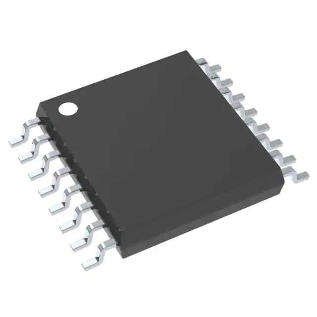
Small TSSOP-16 Package
APPLICATIONS
•
•
•
•
Bridge Sensors
Remote 4-20mA Transmitters
Strain, Load, and Weigh Scales
Automotive Sensors
EVALUATION TOOLS
•
Hardware Designer’s Kit (PGA309EVM)
– Temperature Eval of PGA309 + Sensor
– Full Programming of PGA309
– Sensor Compensation Analysis Tool
The all-analog signal path contains a 2x2 input
multiplexer (mux), auto-zero programmable-gain
instrumentation amplifier, linearization circuit, voltage
reference, internal oscillator, control logic, and an
output amplifier. Programmable level shifting
compensates for sensor dc offsets.
The core of the PGA309 is the precision, low-drift, no
1/f noise Front-End PGA (Programmable Gain
Amplifier). The overall gain of the Front-End PGA +
Output Amplifier can be adjusted from 2.7V/V to
1152V/V. The polarity of the inputs can be switched
through the input mux to accommodate sensors with
unknown polarity output. The Fault Monitor circuit
detects and signals sensor burnout, overload, and
system fault conditions.
For detailed application information, see the PGA309
User's Guide (SBOU024) available for download at
www.ti.com.
VS
Nonlinear
Bridge
VEXC
PGA309
Linearization
Circuit
Transducer
P
0
psi
Ref
Lin DAC
Analog Sensor Linearization
50
Fault
Monitor
Auto- Zero
PGA
Over/Under
Scale Limiter
Linear
VOUT
Analog Signal Conditioning
+125°C
Digital
Int Temp
Temperature
Compensation
T
-40°C
Ext Temp
Ext Temp
Digital Cal
Temp
ADC
Control Register
Interface Circuitry
EEPROM
(SOT23-5)
1
2
Please be aware that an important notice concerning availability, standard warranty, and use in critical applications of Texas
Instruments semiconductor products and disclaimers thereto appears at the end of this data sheet.
All trademarks are the property of their respective owners.
PRODUCTION DATA information is current as of publication date.
Products conform to specifications per the terms of the Texas
Instruments standard warranty. Production processing does not
necessarily include testing of all parameters.
Copyright © 2003–2011, Texas Instruments Incorporated
�PGA309
SBOS292C – DECEMBER 2003 – REVISED JANUARY 2011
www.ti.com
This integrated circuit can be damaged by ESD. Texas Instruments recommends that all integrated circuits be handled with
appropriate precautions. Failure to observe proper handling and installation procedures can cause damage.
ESD damage can range from subtle performance degradation to complete device failure. Precision integrated circuits may be more
susceptible to damage because very small parametric changes could cause the device not to meet its published specifications.
PACKAGE/ORDERING INFORMATION (1)
(1)
PRODUCT
PACKAGE-LEAD
PACKAGE
DESIGNATOR
PACKAGE
MARKING
PGA309
TSSOP-16
PW
PGA309
For the most current package and ordering information see the Package Option Addendum at the end of this document, or see the TI
web site at www.ti.com.
ABSOLUTE MAXIMUM RATINGS (1)
Over operating free-air temperature range, unless otherwise noted.
PARAMETER
Supply Voltage, VSD, VSD
Input Voltage, VIN1, VIN2
(2)
PGA309
UNIT
+7.0
V
–0.3 to VSA +0.3
V
Input Current, VFB, VOUT
±150
mA
Input Current
±10
mA
Output Current Limit
50
mA
Storage Temperature Range
–60 to +150
°C
Operating Temperature Range
–55 to +150
°C
Junction Temperature
ESD Ratings
(1)
(2)
2
Human Body Model (HBM)
+150
°C
4
kV
Stresses above these ratings may cause permanent damage. Exposure to absolute maximum conditions for extended periods may
degrade device reliability. These are stress ratings only, and functional operation of the device at these or any other conditions beyond
those specified is not implied.
Input terminals are diode-clamped to the power-supply rails. Input signals that can swing more than 0.5V beyond the supply rails should
be current limited to 10mA or less.
Submit Documentation Feedback
Copyright © 2003–2011, Texas Instruments Incorporated
Product Folder Link(s): PGA309
�PGA309
www.ti.com
SBOS292C – DECEMBER 2003 – REVISED JANUARY 2011
ELECTRICAL CHARACTERISTICS
Boldface limits apply over the specified temperature range, TA = –40°C to +125°C.
At TA = +25°C, VSA= VSD = +5V (VSA = VSUPPLY ANALOG, VSD = VSUPPLY DIGITAL; VSA must equal VSD), GNDD = GNDA = 0, and VREF
= REFIN/REFOUT = +5V, unless otherwise noted.
PGA309
PARAMETER
CONDITIONS
MIN
TYP
MAX
UNIT
Front-End PGA + Output Amplifier
VOUT/VIN Differential Signal Gain Range (1)
Fine gain adjust = 1
8 to 1152
V/V
210
nV/√Hz
0.5
V/ms
ms
Front-End PGA Gains: 4, 8, 16, 23.27, 32, 42.67, 64, 128
Output Amplifier gains: 2, 2.4, 3, 3.6, 4.5, 6, 9
Input Voltage Noise Density
f = 1kHz
VOUT Slew Rate
VOUT Settling Time (0.01%)
VOUT/VIN Differential gain = 8, RL = 5kΩ || 200pF
6
VOUT Settling Time (0.01%)
VOUT/VIN Differential gain = 191, RL = 5kΩ || 200pF
4.1
ms
0.002
%FSR
VSA = VSD = VEXC = +5V
1 to 245
mV/V
Coarse offset adjust disabled
±3
VOUT Nonlinearity
External Sensor Output Sensitivity
Front-End PGA
Auto-Zero Internal Frequency
Offset Voltage (RTI) (2)
7
vs Temperature
±0.2
vs Supply Voltage, VSA
vs Common-Mode Voltage
kHz
±50
±2
GF = Front-End PGA gain
Linear Input Voltage Range (3)
1500/GF
0.2
Input Bias Current
0.1
mV
mV/°C
mV/V
6000/GF
mV/V
VSA − 1.5
V
1.5
nA
Input Impedance: Differential
30 || 6
GΩ || pF
Input Impedance: Common-Mode
50 || 20
GΩ || pF
0.1Hz to 10Hz, GF = 128
4
mVPP
4, 8, 16, 23.27, 32, 42.67, 64, 128
4 to 128
GF = 4 to 42
0.2
±1
%
GF = 64
0.25
±1.2
%
GF = 128
0.3
±1.6
Input Voltage Noise
PGA Gain
Gain Range Steps
Initial Gain Error
vs Temperature
10
%
ppm/°C
0.05 to VSA − 0.1
V
Gain = 4
400
kHz
Gain = 128
60
kHz
Output Voltage Range
Bandwidth
V/V
Coarse Offset Adjust
(RTI of Front-End PGA)
Range
±(14)(VREF)(0.00085)
±56
vs Temperature
Drift
±14 steps, 4-bit + sign
±59.5
±64
mV
0.004
%/°C
4
mV
Fine Offset Adjust (Zero DAC)
(RTO of the Front-End PGA) (2)
Programming Range
Output Voltage Range
Resolution
65,536 steps, 16-bit DAC
0
VREF
0.1
VSA – 0.1
V
V
73
mV
Integral Nonlinearity
20
LSB
Differential Nonlinearity
0.5
LSB
Gain Error
0.1
%
Gain Error Drift
10
ppm/°C
Offset
5
mV
Offset Drift
10
mV/°C
(1)
(2)
(3)
PGA309 total differential gain from input (VIN1 – VIN2) to output (VOUT). VOUT / (VIN1 – VIN2) = (Front-end PGA gain) × (Output Amplifier
gain) × (Gain DAC).
RTI = Referred-to-input. RTO = referred to output.
Linear input range is the allowed min/max voltage on the VIN1 and VIN2 pins for the input PGA to continue to operate in a linear region.
The allowed common-mode and differential voltage depends on gain and offset settings. Refer to the Gain Scaling section for more
information.
Submit Documentation Feedback
Copyright © 2003–2011, Texas Instruments Incorporated
Product Folder Link(s): PGA309
3
�PGA309
SBOS292C – DECEMBER 2003 – REVISED JANUARY 2011
www.ti.com
ELECTRICAL CHARACTERISTICS (continued)
Boldface limits apply over the specified temperature range, TA = –40°C to +125°C.
At TA = +25°C, VSA= VSD = +5V (VSA = VSUPPLY ANALOG, VSD = VSUPPLY DIGITAL; VSA must equal VSD), GNDD = GNDA = 0, and VREF
= REFIN/REFOUT = +5V, unless otherwise noted.
PGA309
PARAMETER
CONDITIONS
MIN
TYP
MAX
UNIT
Output Fine Gain Adjust (Gain DAC)
Range
0.33 to 1
V/V
10
mV/V
Integral Nonlinearity
20
LSB
Differential Nonlinearity
0.5
LSB
Resolution
65,536 steps, 16-bit DAC
Output Amplifier
Offset Voltage (RTI of Output Amplifier) (4)
vs Temperature
vs Supply Voltage, VSA
3
mV
5
mV/°C
30
Common-Mode Input Range
0
Input Bias Current
mV/V
VS – 1.5
100
V
pA
Amplifier Internal Gain
Gain Range Steps
Initial Gain Error
vs Temperature
Output Voltage Range (5)
2, 2.4, 3, 3.6, 4.5, 6, 9
2 to 9
2, 2.4, 3.6
0.25
±1
%
4.5
0.3
±1.2
%
6
0.4
±1.5
%
9
0.6
±2.0
2, 2.4, 3.6
5
ppm/°C
4.5
5
ppm/°C
6
15
ppm/°C
9
30
RL = 10kΩ
0.1
Open-Loop Gain
Gain-Bandwidth Product
deg
AC Small-signal, open-loop, f = 1MHz, IO = 0
675
Ω
VREF = 4.096
Ratio of VREF, Register 5—bits D5, D4, D3 = ‘000’
0.9708
Ratio of VREF, Register 5—bits D5, D4, D3 = ‘001’
0.9610
Ratio of VREF, Register 5—bits D5, D4, D3 = ‘010’
0.9394
Ratio of VREF, Register 5—bits D5, D4, D3 = ‘011’
0.9160
Ratio of VREF, Register 5—bits D5, D4, D3 = ‘100’
0.9102
Ratio of VREF, Register 5—bits D5, D4, D3 = ‘101’
0.7324
0.5528
+6
Over-Scale Comparator Offset Drift
+60
+114
+0.37
Ratio of VREF, Register 5—bits D2, D1, D0 = ‘111’
0.0605
Ratio of VREF, Register 5—bits D2, D1, D0 = ‘110’
0.0547
Ratio of VREF, Register 5—bits D2, D1, D0 = ‘101’
0.0507
Ratio of VREF, Register 5—bits D2, D1, D0 = ‘100’
0.0449
Ratio of VREF, Register 5—bits D2, D1, D0 = ‘011’
0.0391
Ratio of VREF, Register 5—bits D2, D1, D0 = ‘010
0.0352
Ratio of VREF, Register 5—bits D2, D1, D0 = ‘001’
0.0293
Ratio of VREF, Register 5—bits D2, D1, D0 = ‘000’
−50
−0.15
Under-Scale Comparator Offset Drift
mV
mV/°C
0.0254
−7
Unde-rScale Comparator Offset
4
dB
MHz
Over-Scale Comparator Offset
(4)
(5)
V
115
2
Ratio of VREF, Register 5—bits D5, D4, D3 = ‘110’
Under-Scale Thresholds
ppm/°C
4.9
45
Over- and Under-Scale Limits
Over-Scale Thresholds
%
Gain = 2, CL = 200pF
Phase Margin
Output Resistance
V/V
+93
mV
mV/°C
RTI = Referred-to-input. RTO = referred to output.
Unless limited by the over/under-scale setting.
Submit Documentation Feedback
Copyright © 2003–2011, Texas Instruments Incorporated
Product Folder Link(s): PGA309
�PGA309
www.ti.com
SBOS292C – DECEMBER 2003 – REVISED JANUARY 2011
ELECTRICAL CHARACTERISTICS (continued)
Boldface limits apply over the specified temperature range, TA = –40°C to +125°C.
At TA = +25°C, VSA= VSD = +5V (VSA = VSUPPLY ANALOG, VSD = VSUPPLY DIGITAL; VSA must equal VSD), GNDD = GNDA = 0, and VREF
= REFIN/REFOUT = +5V, unless otherwise noted.
PGA309
PARAMETER
CONDITIONS
MIN
TYP
MAX
UNIT
Fault Monitor Circuit
(6)
VSA− 1.2 or VEXC− 0.1
V
100
mV
A1SAT_HI, A2SAT_HI Comparator Threshold
VSA− 0.12
V
A1SAT_LO, A2SAT_LO Comparator Threshold
VSA− 0.12
V
A3_VCM Comparator Threshold
VSA− 1.2
V
20
mV
INP_HI, INN_HI Comparator Threshold
See
INP_LO, INN_LO Comparator Threshold
40
Comparator Hysteresis
Internal Voltage Reference
VREF1
Register 3, bit D9 = 1
2.46
2.5
VREF1 Drift vs Temperature
VREF2
2.53
V
+10
IPU
Register 3, bit D9 = 0
4.0
VREF2 Drift vs Temperature
Input Current REFIN/REFOUT
Output Current REFIN/REFOUT
ppm/°C
4.096
4.14
V
+10
±7
ppm/°C
Internal VREF disabled
100
mA
VSA > 2.7V for VREF = 2.5V
1
mA
VSA > 4.3V for VREF = 4.096V
1
mA
±2
°C
Temperature Sense Circuitry (ADC)
Internal Temperature Measurement
Register 6, bit D9 = 1
xx Accuracy
xx Resolution
12-Bit + sign, twos complement data format
±0.0625
−55
xx Temperature Measurement Range
xx Conversion Rate
°C
+150
R1, R0 = ‘11’, 12-bit + sign resolution
°C
24
ms
Temperature ADC
External Temperature Mode
Temp PGA + Temp ADC
xx Gain Range Steps
GPGA = 1, 2, 4, 8
1 to 8
GND −0.2
V/V
VSA +0.2
V
xx Analog Input Voltage Range
Temperature ADC Internal REF (2.048V)
Register 6, bit D8 = 1
(+Input) − (−Input)
xx Full-Scale Input Voltage
±2.048/GPGA
V
2.8/GPGA
MΩ
GPGA = 1
3.5
MΩ
GPGA = 2
3.5
MΩ
GPGA = 4
1.8
MΩ
GPGA = 8
0.9
MΩ
R1, R0 = ‘00’, ADC2X = ‘0’, conversion time = 8ms
11
Bits + Sign
R1, R0 = ‘01’, ADC2X = ‘0’, conversion time = 32ms
13
Bits + Sign
R1, R0 = ‘10’, ADC2X = ‘0’, conversion time = 64ms
14
Bits + Sign
R1, R0 = ‘11’, ADC2X = ‘0’, conversion time = 128ms
15
Bits + Sign
xx Differential Input Impedance
xx Common-Mode Input Impedance
xx Resolution
xx Integral Nonlinearity
xx Offset Error
xx Offset Drift
(6)
0.004
%
GPGA = 1
1.2
mV
GPGA = 2
0.7
mV
GPGA = 4
0.5
mV
GPGA = 8
0.4
mV
GPGA = 1
1.2
mV/°C
GPGA = 2
0.6
mV/°C
GPGA = 4
0.3
mV/°C
GPGA = 8
0.3
mV/°C
When VEXC is enabled, a minimum reference selector circuit becomes the reference for the comparator threshold. This minimum
reference selector circuit uses VEXC − 100mV and VSA − 1.2V and compares the VINX pin to the lower of the two references. This
configuration ensures accurate fault monitoring in conditions where VEXC might be higher or lower than the input CMR of the PGA input
amplifier relative to VSA.
Submit Documentation Feedback
Copyright © 2003–2011, Texas Instruments Incorporated
Product Folder Link(s): PGA309
5
�PGA309
SBOS292C – DECEMBER 2003 – REVISED JANUARY 2011
www.ti.com
ELECTRICAL CHARACTERISTICS (continued)
Boldface limits apply over the specified temperature range, TA = –40°C to +125°C.
At TA = +25°C, VSA= VSD = +5V (VSA = VSUPPLY ANALOG, VSD = VSUPPLY DIGITAL; VSA must equal VSD), GNDD = GNDA = 0, and VREF
= REFIN/REFOUT = +5V, unless otherwise noted.
PGA309
PARAMETER
CONDITIONS
MIN
TYP
MAX
UNIT
Temperature ADC. continued
xx Offset vs VSA
GPGA = 1
800
mV/V
GPGA = 2
400
mV/V
GPGA = 4
200
mV/V
GPGA = 8
150
xx Gain Error
xx Gain Error Drift
xx Noise
All gains
Temp ADC Ext. REF (VREFT = VREF, VEXC, or VSA)
xx Resolution
xx Offset Drift
At dc and GPGA = 8
105
dB
At dc and GPGA = 1
100
dB
Register 6, bit D8 = 0
±VREFT/GPGA
V
2.4/GPGA
MΩ
GPGA = 1
8
MΩ
GPGA = 2
8
MΩ
GPGA = 4
8
MΩ
GPGA = 8
8
MΩ
R1, R0 = ‘00’, ADC2X = ‘0’, conversion time = 6ms
11
Bits + Sign
R1, R0 = ‘01’, ADC2X = ‘0’, conversion time = 24ms
13
Bits + Sign
R1, R0 = ‘10’, ADC2X = ‘0’, conversion time = 50ms
14
Bits + Sign
R1, R0 = ‘11’, ADC2X = ‘0’, conversion time = 100ms
15
Bits + Sign
0.01
%
GPGA = 1
2.5
mV
GPGA = 2
1.25
mV
GPGA = 4
0.7
mV
GPGA = 8
0.3
mV
GPGA = 1
1.5
mV/°C
GPGA = 2
1.0
mV/°C
GPGA = 4
0.7
mV/°C
GPGA = 8
0.6
mV/°C
xx Gain Error
xx Gain Error Drift
xx Gain vs VSA
xx Common-Mode Rejection
External Temperature Current Excitation
ITEMP
−0.2
%
2
ppm/°C
80
ppm/V
At dc and GPGA = 8
100
dB
At dc and GPGA = 1
85
dB
Register 6, bit D11 = 1
xx Current Excitation
5.8
xx Temperature Drift
xx Voltage Compliance
6
ppm/°C
LSB
xx Integral Nonlinearity
xx Offset Error
50
ppm/V
xx Differential Input Impedance
xx Common-Mode Input Impedance
%
5
80
(+Input) − (−Input)
xx Full-Scale Input Voltage
0.50
100pF) and/or for using external gain setting resistors for the output amplifier.
9
TEST
10
VSD
11
GNDD
12
PRG
Single-wire interface program pin. UART-type interface for digital calibration of the PGA309 over a
single wire. Can be connected to VOUT for a three-lead (VS, GND, VOUT) digitally-programmable sensor
assembly.
13
SCL
Clock input/output for Two-Wire, industry-standard compatible interface for reading and writing digital
calibration and configuration from external EEPROM. Can also communicate directly to the registers in
the PGA309 through the Two-Wire, industry-standard compatible interface.
14
SDA
Data input/output for Two-Wire, industry-standard compatible interface for reading and writing digital
calibration and configuration from external EEPROM. Can also communicate directly to the registers in
the PGA309 through the Two-Wire, industry-standard compatible interface.
15
TEMPIN
16
REFIN/REFOUT
Test/External controller mode pin. Pull to GNDD in normal mode.
Digital voltage supply. Connect to digital voltage supply. To be within 200mV of VSA.
Digital ground. Connect to digital ground return path for VSD. Should be same as GNDA.
External temperature signal input. PGA309 can be configured to read a bridge current sense resistor
as an indicator of bridge temperature, or an external temperature sensing device such as diode
junction, RTD, or thermistor. This input can be internally gained by 1, 2, 4, or 8. In addition, this input
can be read differentially with respect to VGNDA, VEXC, or the internal/external VREF. There is also an
internal, register-selectable, 7mA current source (ITEMP) that can be connected to TEMPIN as an RTD,
thermistor, or diode excitation source.
Reference input/output pin. As an output, the internal reference (selectable as 2.5V or 4.096V) is
available for system use on this pin. As an input, the internal reference may be disabled and an
external reference can then be applied as the reference for the PGA309.
Submit Documentation Feedback
Copyright © 2003–2011, Texas Instruments Incorporated
Product Folder Link(s): PGA309
�PGA309
www.ti.com
SBOS292C – DECEMBER 2003 – REVISED JANUARY 2011
TYPICAL CHARACTERISTICS
At TA = +25°C, VSA = VSD = +5V (VSA = VSUPPLY ANALOG, VSD = VSUPPLY DIGITAL, VSA must equal VSD), GNDD = GNDA = 0, and
VREF = REFIN/REFOUT = +5V, unless otherwise noted.
VREF vs TEMPERATURE
IB CURRENT vs TEMPERATURE
4.090
1.0
0.5
4.085
0
Average, nA
-0.5
IB (nA)
VREF (V)
4.080
4.075
Average
-1.0
-1.5
4.070
-2.0
4.065
-2.5
4.060
-55 -35 -15
5
25
45
65
85
-3.0
-55 -35 -15
105 125 145
5
Temperature (°C)
Figure 1.
9
8
60
Average
85
105 125 145
RTO of Front- End PGA
50
40
CMRR (dB)
ITEMP (mA)
65
COMMON-MODE REJECTION RATIO vs FREQUENCY
70
6
5
4
3
30
20
10
0
2
-10
1
-20
0
-55 -35 -15
-30
5
25
45
65
85
10
105 125 145
100
1k
10k
100k
1M
Frequency (Hz)
Temperature (°C)
Figure 3.
Figure 4.
POWER-SUPPLY REJECTION RATIO vs FREQUENCY
CLOSED−LOOP GAIN vs FREQUENCY
90
80
80
70
GOUTAMP = Output Amplifier Gain
GOUTAMP = 9V/V
GFRONT = 128V/V
60
Gain (dB)
60
PSRR (dB)
45
Figure 2.
ITEMP CURRENT vs TEMPERATURE
7
25
Temperature (°C)
50
40
30
Small-Signal
VREF and VEXT Enabled
VREF = 2.5V
PSRR at VOUT
20
10
0
GOUTAMP = 9V/V
GFRONT = 32V/V
40
20
GOUTAMP = 2V/V
GFRONT = 32V/V
GOUTAMP = 2V/V
GFRONT = 8V/V
0
-10
10
100
1k
10k
100k
1M
10
100
1k
10k
100k
1M
Frequency (Hz)
Frequency (Hz)
Figure 5.
Figure 6.
Submit Documentation Feedback
Copyright © 2003–2011, Texas Instruments Incorporated
Product Folder Link(s): PGA309
9
�PGA309
SBOS292C – DECEMBER 2003 – REVISED JANUARY 2011
www.ti.com
TYPICAL CHARACTERISTICS (continued)
At TA = +25°C, VSA = VSD = +5V (VSA = VSUPPLY ANALOG, VSD = VSUPPLY DIGITAL, VSA must equal VSD), GNDD = GNDA = 0, and
VREF = REFIN/REFOUT = +5V, unless otherwise noted.
VOUT SWING TO RAIL vs ILOAD
IQ vs TEMPERATURE
VS
1.6
VS - 0.1
1.4
VS - 0.2
VS = 5V
VS = 2.7V
VS - 0.3
All Blocks Enabled
1.2
VS - 0.4
IQ (mA)
1.0
VS - 0.5
0.5
0.4
0.4
VS = 2.7V
0.2
Ref, Exc, and ADC Disabled
0.6
VS = 5V
0.3
0.8
0.2
0.1
0
0
5
10
15
20
0
-55 -35 -15
25
5
ILOAD (mA)
Figure 7.
0.2
0.3
0
0.2
Total Error (% of FS)
Temp ADC Error (°C)
0.4
-0.2
-0.4
-0.6
-0.8
-1.0
45
105 125 145
65
85
105 125 145
Reg 6 = 0503h
VREF = 2.048V Internal
(Temp ADC Internal)
15-Bit + Sign
Reg 6 = 0433h
VREF = 2.5V Internal
15-Bit + Sign
0
-0.1
Reg 6 = 0430h
VREF = 2.5V Internal
11-Bit + Sign
Reg 6 = 0403h
VREF = 5V Internal
15-Bit + Sign
-0.3
25
85
0.1
-0.2
5
65
TEMPERATURE ADC ERROR (EXTERNAL MODES)
0.4
-1.2
-55 -35 -15
45
Figure 8.
TEMPERATURE ADC ERROR (INTERNAL MODE)
-0.4
-100 -80 -60
-40 -20
0
20
40
60
80
Figure 9.
Figure 10.
VREF NOISE
(0.1Hz TO 10Hz)
VOUT NOISE
(0.1Hz TO 10Hz PEAK-TO-PEAK NOISE)
VIN = +61mV
CLK_CFG = 00 (default)
VREF = 4.096V
G = 1152
Coarse Offset = -59mV
1mV/div
50mV/div
100
Input Signal (% FS of VREF)
Actual Die Temperature (°C)
Measured After Bandpass Filter
0.1Hz Second-Order High-Pass
10Hz Fourth-Order Low-Pass
Measured After Bandpass Filter
0.1Hz Second-Order High-Pass
10Hz Fourth-Order Low-Pass
1s/div
1s/div
Figure 11.
10
25
Temperature (°C)
Figure 12.
Submit Documentation Feedback
Copyright © 2003–2011, Texas Instruments Incorporated
Product Folder Link(s): PGA309
�PGA309
www.ti.com
SBOS292C – DECEMBER 2003 – REVISED JANUARY 2011
TYPICAL CHARACTERISTICS (continued)
At TA = +25°C, VSA = VSD = +5V (VSA = VSUPPLY ANALOG, VSD = VSUPPLY DIGITAL, VSA must equal VSD), GNDD = GNDA = 0, and
VREF = REFIN/REFOUT = +5V, unless otherwise noted.
INPUT VOLTAGE NOISE DENSITY
INPUT VOLTAGE NOISE DENSITY
1
Coarse Offset Adjust = -59mV
VIN = +61mV
CLK_CFG = 00 (default)
Coarse Offset Adjust = 0mV
CLK_CFG = 00 (default)
eND (mV/ÖHz), RTI
eND (mV/ÖHz), RTI
10
1
0.1
0.1
0.01
0.01
1
10
100
1k
10k
1
50k
Frequency (Hz)
10
100
1k
10k
100k
Frequency (Hz)
Figure 13.
Figure 14.
LARGE-SIGNAL STEP RESPONSE
LARGE-SIGNAL STEP RESPONSE
Gain = 1152
VOUT (500mV/div)
VOUT (500mV/div)
Gain = 8
Time (10ms/div)
Time (10ms/div)
Figure 15.
Figure 16.
SMALL-SIGNAL STEP RESPONSE
SMALL-SIGNAL STEP RESPONSE
Gain = 256
VOUT (50mV/div)
VOUT (50mV/div)
Gain = 8
Time (10ms/div)
Time (10ms/div)
Figure 17.
Figure 18.
Submit Documentation Feedback
Copyright © 2003–2011, Texas Instruments Incorporated
Product Folder Link(s): PGA309
11
�PGA309
SBOS292C – DECEMBER 2003 – REVISED JANUARY 2011
www.ti.com
TYPICAL CHARACTERISTICS (continued)
At TA = +25°C, VSA = VSD = +5V (VSA = VSUPPLY ANALOG, VSD = VSUPPLY DIGITAL, VSA must equal VSD), GNDD = GNDA = 0, and
VREF = REFIN/REFOUT = +5V, unless otherwise noted.
CAPACITIVE LOAD DRIVE
OVERVOLTAGE RECOVERY
VOUT
VIN (200mV/div), VOUT (1V/div)
0.5% Settling Time (ms)
25
GOUTAMP = 2V/V
20
15
GOUTAMP = 3.6V/V
GOUTAMP = 9V/V
10
5
VIN
0
0
500
1000
1500
2000
Time (100ms/div)
2500
CLOAD (pF)
Figure 19.
Figure 20.
OUTPUT AMPLIFIER
OPEN-LOOP GAIN/PHASE vs FREQUENCY
120
CL = 100pF
RL = 4.7kW
100
ZERO DAC TYPICAL ERROR vs CODE
45
20
15
0
Unit 2
-45
60
-90
40
-135
20
-180
5
Error (LSB)
80
Phase (°)
AOL (dB)
10
0
Unit 1
-5
-10
-15
0
0.1
1
10
100
1k
10k
100k
1M
-225
10M
-20
0
10000
20000 30000
Frequency (Hz)
40000
50000 60000
70000
Code (LSB)
Figure 21.
Figure 22.
GAIN DAC TYPICAL ERROR vs CODE
20
15
Error (LSB)
10
5
0
-5
-10
-15
-20
0
10000
20000 30000
40000
50000 60000
70000
Code (LSB)
Figure 23.
12
Submit Documentation Feedback
Copyright © 2003–2011, Texas Instruments Incorporated
Product Folder Link(s): PGA309
�PGA309
www.ti.com
SBOS292C – DECEMBER 2003 – REVISED JANUARY 2011
FUNCTIONAL DESCRIPTION
OVERVIEW
The PGA309 is a programmable analog signal
conditioner designed for resistive bridge sensor
applications. It is a complete signal conditioner with
bridge excitation, initial span and offset adjustment,
temperature adjustment of span and offset,
internal/external temperature measurement capability,
output over-scale and under-scale limiting, fault
detection, and digital calibration. The PGA309, in a
calibrated sensor module, can reduce errors to the
level approaching the bridge sensor repeatability. See
Figure 24 for a block diagram of the PGA309.
Following is a brief overview of each major function.
of
the
PGA309
is
Table 1. PGA309 Adjustment Capability
FSS (full-scale sensitivity)
1mV/V to 245mV/V
Span TC
Over ±3300ppmFS/°C(1)
Span TC nonlinearity
≥ 10%
Zero offset
±200%FS(2)
Zero offset TC
Over ±3000ppmFS/°C(2)
Zero offset TC nonlinearity
≥ 10%
Sensor impedance
Down to 200Ω(3)
Following the fine gain adjust stage is the Output
Amplifier that provides additional programmable gain.
Two key output amplifier connections, VFB and VSJ,
are brought out on the PGA309 for application
flexibility. These connections allow for an accurate
conditioned signal voltage while also providing a
means for PGA309 output overvoltage and large
capacitive loading for RFI/EMI filtering required in
many end applications.
OFFSET ADJUSTMENT
SENSOR ERROR ADJUSTMENT RANGE
The adjustment capability
summarized in Table 1.
Converter (Temp ADC). In order to compensate for
second-order and higher drift nonlinearity, the span
drift can be fitted to piecewise linear curves during
calibration with the coefficients stored in an external
nonvolatile EEPROM lookup table.
1. Depends on the temperature sensing scheme.
2. Combined coarse and fine offset adjust.
3. Lower impedance possible by using a dropping
resistor in series with the bridge.
GAIN SCALING
The core of the PGA309 is the precision low-drift and
no 1/f noise Front-End PGA. The overall gain of the
Front-End PGA + Output Amplifier can be adjusted
from 2.7V/V to 1152V/V. The polarity of the inputs
can be switched through the 2x2 input mux to
accommodate sensors with unknown polarity output.
The Front-End PGA provides initial coarse signal gain
using a no 1/f noise, auto-zero instrumentation
amplifier. The fine gain adjust is accomplished by the
16-bit attenuating Gain Digital-to-Analog Converter
(Gain DAC). This Gain DAC is controlled by the data
in the Temperature Compensation Lookup Table
driven by the Temperature Analog-to-Digital
The sensor offset adjustment is performed in two
stages. The input-referred Coarse Offset Adjust DAC
has approximately a ±60mV offset adjustment range
for a selected VREF of 5V. The fine offset and the
offset drift are canceled by the 16-bit Zero DAC that
sums the signal with the output of the front-end
instrumentation amplifier. Similar to the Gain DAC,
the input digital values of the Zero DAC are controlled
by the data in the Temperature Compensation
Lookup Table, stored in external EEPROM, driven by
the Temp ADC. The programming range of the Zero
DAC is 0V to VREF with an output range of 0.1V to
VSA – 0.1V.
VOLTAGE REFERENCE
The PGA309 contains a precision low-drift voltage
reference (selectable for 2.5V or 4.096V) that can be
used for external circuitry through the REFIN/REFOUT
pin. This same reference is used for the Coarse
Offset Adjust DAC, Zero DAC, Over/Under-Scale
Limits and sensor excitation/linearization through the
VEXC pin. When the internal reference is disabled, the
REFIN/REFOUT pin should be connected to an
external reference or to VSA for ratiometric-scaled
systems.
SENSOR EXCITATION AND LINEARIZATION
A dedicated circuit with a 7-bit + sign DAC for sensor
voltage excitation and linearization is provided on the
PGA309. This block scales the reference voltage and
sums it with a portion of the PGA309 output to
compensate the positive or negative bow-shaped
nonlinearity exhibited by many sensors over their
applied pressure range. Sensors not requiring
linearization can be connected directly to the supply
(VSA) or to the VEXC pin with the Linearization DAC
(Lin DAC) set to zero.
Submit Documentation Feedback
Copyright © 2003–2011, Texas Instruments Incorporated
Product Folder Link(s): PGA309
13
�PGA309
SBOS292C – DECEMBER 2003 – REVISED JANUARY 2011
www.ti.com
+5V
VSD
VSA
REFIN/REFOUT
PGA309
VREF
Power-On
Reset
KREF
Band-Gap
Voltage
Reference
VEXC
S
VOUT
KLIN
Linearization
DAC
VFB
SDA
Interface and Control
Circuitry
Internal
Temp Sense
VTEMP
TEMPIN
Temp ADC
Signals Mux
+5V
SCL
Two-Wire
EEPROM
(SOT23-5)
Temperature
ADC
Temperature ADC
Input Select
SpanTC and OffsetTC Adjust Lookup
Table with interpolation
Coarse
Offset Adjust
PRG
Fine Offset
Adjust
Zero
DAC
VOS
Over-/UnderScale Limits
VIN2
Bridge
Sensor
2x2 Multiplexer
VIN1
Front-End
PGA Out
Front-End PGA
(Gain 4 to 128)
VOUT
Fault Out
VOUT FILT
Fine Gain
Adjust
Gain
DAC
VOUT
Output
Amp
RISO
100W
CL
10nF
RTEMP
TEST
Fault Conditions
Monitoring Circuit
Fault
Out
Int/Ext
Feedback
VFB
VFB
RFB
100W
Test Logic
Output Coarse
Gain Adjust
(2 to 9)
CF
150pF
VSJ
GNDA
GNDD
Figure 24. Simplified Diagram of the PGA309 in a Typical Configuration
14
Submit Documentation Feedback
Copyright © 2003–2011, Texas Instruments Incorporated
Product Folder Link(s): PGA309
�PGA309
www.ti.com
SBOS292C – DECEMBER 2003 – REVISED JANUARY 2011
ADC FOR TEMPERATURE SENSING
The temperature sense circuitry drives the
compensation for the sensor span and offset drift.
Either internal or external temperature sensing is
possible. The temperature can be sensed in one of
the following ways:
• Bridge impedance change (excitation current
sense, in the positive or negative part of the
bridge), for sensors with large temperature
coefficient of resistance (TCR > 0.1%/°C).
• On-chip PGA309 temperature, when the chip is
located sufficiently close to the sensor.
• External diode, thermistor, or RTD placed on the
sensor membrane. An internal 7mA current source
may be enabled to excite these types of
temperature sensors.
The temperature signal is digitized by the onboard
Temp ADC. The output of the Temp ADC is used by
the control digital circuit to read the data from the
Lookup Table in an external EEPROM, and set the
output of the Gain DAC and the Zero DAC to the
calibrated values as temperature changes.
An additional function provided through the Temp
ADC is the ability to read the VOUT pin back through
the Temp ADC input mux. This provides flexibility for
a digital output through either One-Wire or Two-Wire
interface, as well as the possibility for an external
microcontroller
to
perform
real-time
custom
calibration of the PGA309.
EXTERNAL EEPROM AND TEMPERATURE
COEFFICIENTS
The PGA309 uses an industry-standard Two-Wire
external EEPROM (typically, a SOT23-5 package). A
1k-bit (minimum) EEPROM is needed when using all
17 temperature coefficients. Larger EEPROMs may
be used to provide space for a serial number, lot
code, or other data.
The first part of the external EEPROM contains the
configuration data for the PGA309, with settings for:
• Register 3—Reference Control and Linearization
• Register 4—PGA Coarse Offset and Gain/Output
Amplifier Gain
• Register
5—PGA
Configuration
and
Over/Under-Scale Limit
• Register 6—Temp ADC Control
This section of the EEPROM contains its own
individual checksum (Checksum1).
The second part of the external EEPROM contains
up to 17 temperature index values and corresponding
temperature coefficients for the Zero DAC and Gain
DAC adjustments with measured temperature, and
also contains its own checksum (Checksum2). The
PGA309 lookup logic contains a linear interpolation
algorithm for accurate DAC adjustments between
stored temperature indexes. This approach allows for
a piecewise linear temperature compensation of up to
17 temperature indexes and associated temperature
coefficients.
If either Checksum1, Checksum2, or both are
incorrect, the output of the PGA309 is set to
high-impedance.
FAULT MONITOR
To detect sensor burnout or a short, a set of four
comparators are connected to the inputs of the
Front-End PGA. If any of the inputs are taken to
within 100mV of ground or VEXC, or violate the input
CMR of the Front-End PGA, then the corresponding
comparator sets a sensor fault flag that causes the
PGA309 VOUT to be driven within 100mV of either VSA
or ground, depending upon the alarm configuration
setting (Register 5—PGA Configuration and
Over/Under-Scale Limit). This will be well above the
set Over-Scale Limit level or well below the set
Under-Scale Limit level. The state of the fault
condition can be read in digital form in Register
8—Alarm Status Register. If the Over/Under-Scale
Limit is disabled, the PGA309 output voltage will still
be driven within 100mV of either VSA or ground,
depending upon the alarm configuration setting.
There are five other fault detect comparators that
help detect subtle PGA309 front-end violations that
could otherwise result in linear voltages at VOUT that
would be interpreted as valid states. These are
especially useful during factory calibration and setup,
and are configured through Register 5—PGA
Configuration and Over/Under-Scale Limit. The
respective status of each can also be read back
through Register 8—Alarm Status Register.
OVER-SCALE AND UNDER-SCALE LIMITSE
The over-scale and under-scale limit circuitry
combined with the fault monitor circuitry provides a
means
for
system
diagnostics.
A
typical
sensor-conditioned output may be scaled for 10% to
90% of the system ADC range for the sensor normal
operating range. If the conditioned pressure sensor is
below 4%, it is considered under-pressure; if over
96%, it is considered over-pressure.
The PGA309 over/under-scale limit circuit can be
programmed individually for under-scale and
over-scale values that clip or limit the PGA309 output.
From a system diagnostic view, 10% to 90% of ADC
range is normal operation, less than 4% is
under-pressure, and greater than 96% is
over-pressure. If the fault detect circuitry is used, a
detected fault will cause the PGA309 output to be
driven to positive or negative saturation.
Submit Documentation Feedback
Copyright © 2003–2011, Texas Instruments Incorporated
Product Folder Link(s): PGA309
15
�PGA309
SBOS292C – DECEMBER 2003 – REVISED JANUARY 2011
www.ti.com
If this fault flag is programmed for high, then greater
than 97% ADC range will be a fault; if programmed
for low. then less than 3% ADC range will be a fault.
In this configuration, the system software can be
used to distinguish between over- or under-pressure
condition, which indicates an out-of-control process,
or a sensor fault.
POWER-UP AND NORMAL OPERATION
The PGA309 has circuitry to detect when the power
supply is applied to the PGA309, and reset the
internal registers and circuitry to an initial state. This
reset also occurs when the supply is detected to be
invalid, so that the PGA309 is in a known state when
the supply becomes valid again. The rising threshold
for this circuit is typically 2.2V and the falling
threshold is typically 1.7V. After the power supply
becomes valid, the PGA309 waits for approximately
25ms and then attempts to read the configuration
data from the external EEPROM device.
If the EEPROM has the proper flag set in address
locations 0 and 1, then the PGA309 continues
reading the first part of the EEPROM; otherwise, the
PGA309 waits for one second before trying again. If
the PGA309 detects no response from the EEPROM,
the PGA309 waits for one second and tries again;
otherwise, the PGA309 tries to free the bus and waits
for 25ms before trying to read the EEPROM again. If
a successful read of the first part of the EEPROM is
accomplished, (including valid Checksum1 data), the
PGA309 triggers the Temp ADC to measure
temperature. For 16-bit resolution results, the
converter takes approximately 125ms to complete a
conversion. Once the conversion is complete, the
PGA309 begins reading the Lookup Table information
from the EEPROM (second part) to calculate the
settings for the Gain DAC and Zero DAC.
The PGA309 reads the entire Lookup Table so that it
can determine if the checksum for the Lookup Table
(Checksum2) is correct. Each entry in the Lookup
Table requires approximately 500ms to read from the
EEPROM. Once the checksum is determined to be
valid, the calculated values for the Gain and Zero
DACs are updated into their respective registers, and
the output amplifier is enabled. The PGA309 then
begins looping through this entire procedure, starting
with reading the EEPROM configuration registers
from the first part of the EEPROM, then starting a
new conversion on the Temp ADC, which then
triggers reading the Lookup Table data from the
second part of the EEPROM. This loop continues
indefinitely.
16
DIGITAL INTERFACE
There are two digital interfaces on the PGA309. The
PRG pin uses a One-Wire, UART-compatible
interface with bit rates from 4.8Kbits/s to 38.4Kbits/s.
The SDA and SCL pins together form an industry
standard Two-Wire interface at clock rates from 1kHz
to 400kHz. The external EEPROM uses the Two-Wire
interface. Communication to the PGA309 internal
registers, as well as to the external EEPROM, for
programming and readback can be conducted
through either digital interface.
It is also possible to connect the One-Wire
communication pin, PRG, to the VOUT pin in true
three-wire sensor modules and still allow for
programming. In this mode, the PGA309 output
amplifier may be enabled for a set time period and
then disabled again to allow sharing of the PRG pin
with the VOUT connection. This allows for both digital
calibration and analog readback during sensor
calibration in a three-wire sensor module.
The Two-Wire interface has timeout mechanisms to
prevent bus lockup from occurring. The Two-Wire
master controller in the PGA309 has a mode that
attempts to free up a stuck-at-zero SDA line by
issuing SCL pulses, even when the bus is not
indicated as idle after a timeout period has expired.
The timeout will only apply when the master portion
of the PGA309 is attempting to initiate a Two-Wire
communication.
PGA309 TRANSFER FUNCTION
Equation 1 shows the mathematical expression that is
used to compute the output voltage, VOUT. This
equation can also be rearranged algebraically to
solve for different terms. For example, during
calibration, this equation is rearranged to solve for
VIN.
(
(
VOUT = [ mux_sign ? VIN + VCoarse_Offset ? GI + VZero_DAC ] ? GD ? GO
(1)
Where:
mux_sign: This term changes the polarity of the
input signal; value is ±1.
VIN: The input signal for the PGA309; VIN1 = VINP,
VIN2 = VINN.
VCoarse_Offset: The coarse offset DAC output
voltage.
GI: Input stage gain.
VZero_DAC: Zero DAC output voltage.
GD: Gain DAC.
GO: Output stage gain.
Submit Documentation Feedback
Copyright © 2003–2011, Texas Instruments Incorporated
Product Folder Link(s): PGA309
�PGA309
www.ti.com
SBOS292C – DECEMBER 2003 – REVISED JANUARY 2011
VSA
REFIN/REFOUT
16
Linearization and VEXC
Gain Adjust
PGA309
VEXC Enable
x0.83
1
ITEMP
7mA
ITEMP Enable
15
VREF
x0.52
VSA
TEMPIN
VREF Internal Set
(2.5V or 4.096V)
x0.124
S
Internal
Temp Sense
Temp ADC
Internal REF
Bandgap
Reference
VREF
Temp ADC
Ref Mux
VEXC
VSA VREF Internal Set
(2.5V or 4.096V)
TEMPIN
RSET
VREFT
VREF
Temp ADC
Input Mux
VEXC
VSD
POR
7-Bit + Sign
Lin DAC
VEXC
10
VSA
VFB
x0.166
VEXC
VSD
3
Temp ADC
REF Select
15-Bit + Sign
Temp ADC
xG
Digital Controls
SDA
VOUT
14
Temp ADC, PGA
(x1, x2, x4, x8)
Control Registers
Alarm Register
Temp Select
Source
Temp ADC Input
Mux Select
PGA Gain Select (1 of 8)
Range of 4 to 128
(with PGA Diff Amp Gain = 4)
Input Mux
Control
VREF
Fine
Offset Adjust
4-Bit +
Sign DAC
VREF
Fine Gain Adjust
(16-Bit)
16-Bit
Zero
DAC
PRG
4R
Auto
Zero
5
A2
12
R
Over-Scale
Limit
Front-End
PGA Output
RF
PGA
Diff Amp
RG
4
RF
Auto
Zero
VINN
VIN1
Input Mux
A1
Front-End PGA
Auto
Zero
R
A3
VREF
16-Bit
3-Bit
DAC
VFB VOUT
Gain
DAC
Output
Amplifier
R
Scale
Limiter
VOUT
7
INT/EXT FB Select
Fault Monitor
Circuit
Alarm Register Inputs
RFO
VFB
6
Output Gain Select (1 of 7)
Range of 2 to 9
TEST
9
SCL
13
Offset TC Adjust and Scan TC Adjust
Look-Up Logic with Interpolation Algorithm
Coarse
Offset Adjust
VINP
VIN2
Interface and
Control Circuitry
RGO
VREF
3-Bit
DAC
Test Logic
Under-Scale
Limit
VSJ
8
2
11
GNDA
GNDD
Figure 25. Detailed Block Diagram
Submit Documentation Feedback
Copyright © 2003–2011, Texas Instruments Incorporated
Product Folder Link(s): PGA309
17
�PGA309
SBOS292C – DECEMBER 2003 – REVISED JANUARY 2011
www.ti.com
REVISION HISTORY
NOTE: Page numbers for previous revisions may differ from page numbers in the current version.
Changes from Revision B (January, 2005) to Revision C
Page
•
Updated document format to current standards ................................................................................................................... 1
•
Deleted lead temperature specification from Absolute Maximum Ratings table .................................................................. 2
•
Added PGA Transfer Function section ............................................................................................................................... 16
18
Submit Documentation Feedback
Copyright © 2003–2011, Texas Instruments Incorporated
Product Folder Link(s): PGA309
�PACKAGE OPTION ADDENDUM
www.ti.com
10-Dec-2020
PACKAGING INFORMATION
Orderable Device
Status
(1)
Package Type Package Pins Package
Drawing
Qty
Eco Plan
(2)
Lead finish/
Ball material
MSL Peak Temp
Op Temp (°C)
Device Marking
(3)
(4/5)
(6)
PGA309AIPWR
ACTIVE
TSSOP
PW
16
2500
RoHS & Green
NIPDAU
Level-1-260C-UNLIM
-40 to 125
PGA
309A
PGA309AIPWT
ACTIVE
TSSOP
PW
16
250
RoHS & Green
NIPDAU
Level-1-260C-UNLIM
-40 to 125
PGA
309A
PGA309AIPWTG4
ACTIVE
TSSOP
PW
16
250
RoHS & Green
NIPDAU
Level-1-260C-UNLIM
-40 to 125
PGA
309A
(1)
The marketing status values are defined as follows:
ACTIVE: Product device recommended for new designs.
LIFEBUY: TI has announced that the device will be discontinued, and a lifetime-buy period is in effect.
NRND: Not recommended for new designs. Device is in production to support existing customers, but TI does not recommend using this part in a new design.
PREVIEW: Device has been announced but is not in production. Samples may or may not be available.
OBSOLETE: TI has discontinued the production of the device.
(2)
RoHS: TI defines "RoHS" to mean semiconductor products that are compliant with the current EU RoHS requirements for all 10 RoHS substances, including the requirement that RoHS substance
do not exceed 0.1% by weight in homogeneous materials. Where designed to be soldered at high temperatures, "RoHS" products are suitable for use in specified lead-free processes. TI may
reference these types of products as "Pb-Free".
RoHS Exempt: TI defines "RoHS Exempt" to mean products that contain lead but are compliant with EU RoHS pursuant to a specific EU RoHS exemption.
Green: TI defines "Green" to mean the content of Chlorine (Cl) and Bromine (Br) based flame retardants meet JS709B low halogen requirements of