PGA970EVM User's Guide
User's Guide
Literature Number: SLDU017
November 2016
�Contents
1
2
3
4
Introduction ......................................................................................................................... 4
Default Configuration ........................................................................................................... 5
Inputs and Output Configurations .......................................................................................... 5
3.1
LVDT Primary and Secondary Drive................................................................................... 5
3.2
Temperature Input
3.3
Voltage Mode Output .................................................................................................... 6
.......................................................................................................
6
OWI .................................................................................................................................... 7
..........................................................................................................
4.1
Activation Pulse
4.2
Data Sent Through OWI................................................................................................. 8
8
5
6
XDS200 and USB2ANY Connectors ........................................................................................ 9
Schematics ........................................................................................................................ 12
2
Table of Contents
SLDU017 – November 2016
Submit Documentation Feedback
Copyright © 2016, Texas Instruments Incorporated
�www.ti.com
List of Figures
1
PGA970EVM ................................................................................................................. 4
2
LVDT Primary and Secondary Drive in the PGA970EVM .............................................................. 5
3
PGA970 in Voltage Mode Configuration .................................................................................. 6
4
OWI Block Diagram
5
OWI Activation Pulse Generated by the PGA970EVM in Voltage Mode ............................................. 8
6
OWI Data at 320 bps; Oscilloscope Probe is Connected at TP21 in the PGA970EVM ............................ 8
7
XDS200 Emulator Connection to the PGA970EVM ..................................................................... 9
8
USB2ANY Connection to the PGA970EVM ............................................................................ 10
9
USB2ANY ................................................................................................................... 10
10
USB2ANY Pinout ........................................................................................................... 11
11
PGA970EVM Main Schematic ............................................................................................ 12
12
Input and Output Schematic .............................................................................................. 13
13
USB2ANY Schematic ...................................................................................................... 14
14
OWI Activation Pulse and Data Schematic ............................................................................. 15
15
OWI Power Amplifier Schematic ......................................................................................... 16
16
Power Supplies Schematic................................................................................................ 17
.........................................................................................................
SLDU017 – November 2016
Submit Documentation Feedback
List of Figures
Copyright © 2016, Texas Instruments Incorporated
7
3
�User's Guide
SLDU017 – November 2016
PGA970EVM User’s Guide
The PGA970EVM provides a platform to test the PGA970 in the QFN package.
1
Introduction
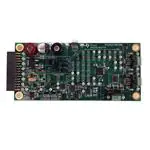
Figure 1 shows the PGA970EVM and its main sections.
XDS200
LVDT
SECONDARY
MODE
POWER
ONE-WIRE INTERFACE
LVDT
PRIMARY
Figure 1. PGA970EVM
The PGA970EVM is divided into six sections:
1. Interface boards and external power:
(a) USB2ANY connector
(b) XDS200 connector (single wire debugger)
(c) Banana connectors to power up EVM
2. Power:
(a) 7.5-V, 5-V, and 3.3-V regulators
3. Mode selection
(a) Voltage mode
(b) 4- to 20-mA loop (3-wire current mode; this section is not placed on the board)
4. OWI circuitry
5. LVDT Primary Driver and Secondary Return
4
PGA970EVM User’s Guide
SLDU017 – November 2016
Submit Documentation Feedback
Copyright © 2016, Texas Instruments Incorporated
�Default Configuration
www.ti.com
2
Default Configuration
The EVM requires a 10- to 30-V input applied to J11 and J12. Clamp the power supply current to 100 mA.
The EVM is shipped configured for voltage mode as shown in Table 1.
Table 1. Default PGA970EVM Jumper Configuration (Voltage Mode)
JUMPERS
VDD
PURPOSE
J18 closed. J16 and J17 open
PGA970 powered up from VPWR (VDD=VPWR)
LVDT Primary
J2 and J7 tied between pins 1 and 2
Drive
External amplifier for P1 and P2 LVDT drive is
bypassed
LVDT
Secondary
Filtering
J1, J4, J6, J9 closed
External filtering and attenuation for secondary
inputs to S1 and S2 bypassed
Output
J11, J12 closed
Voltage mode with 100-nF load, with capacitive
load compensation
Gate Drive
J19 closed
GATE pin grounded
3
Inputs and Output Configurations
3.1
LVDT Primary and Secondary Drive
The PGA970EVM provides screw terminal connectors J3, J5, and J8 interfacing with the Primary and
Secondary of an LVDT. In the default configuration, the Waveform Output Pins of the PGA970, P1 and
P2, are tied directly to these terminals. The alternative Jumper configuration allows the user to amplify the
waveform for higher voltage LVDT applications. This amplifier provides a gain of 16.1 V/V. In a typical
PGA970 Waveform configuration of 0.375 V Amplitude from the Waveform DAC and 1.67 V/V Waveform
Gain, this output of this external amplifier will allow the user to have a 20 V peak-to-peak, 7.07 Vrms
signal at the terminal connection. If additional current driving capabilities are needed in a resolver or
similar, large-load applications, we provided the footprint for an additional drive stage to handle such
loads.
The LVDT Secondary side of the PGA970EVM provides footprints to allow for any necessary external
filtering or decoupling before being tied to the PGA970 S1 and S2 inputs. In the case that the external
amplifier is used on the primary side, the removing jumpers J1, J4, J6, and J9 will provide both decoupling
and resistance in the path to attenuate the signal. A resistor divider is created with the internal impedance
of these pins, allowing the return signal to be within a measurable amplitude of the ADC.
Figure 2 shows a simple functionality diagram of the Primary and Secondary Drive capabilities on the
PGA970EVM.
BIAS
P1
+
OPA166 2
Exte rnal
LVDT
TO S1P
±
0.47 …F
31.6 k
47 nF 43 k
510 k
PGA970
TO S1N
47 nF 43 k
BIAS
P2
OPA166 2
±
0.47 …F
TO S2P
+
47 nF 43 k
31.6 k
TO S2N
510 k
47 nF 43 k
Figure 2. LVDT Primary and Secondary Drive in the PGA970EVM
SLDU017 – November 2016
Submit Documentation Feedback
PGA970EVM User’s Guide
Copyright © 2016, Texas Instruments Incorporated
5
�Inputs and Output Configurations
3.2
www.ti.com
Temperature Input
The PGA970EVM does not have on-board stimulus for the temperature inputs of the PGA970. However,
the AIN pin, connected to TP2, can be used to provide an external single-ended connection to a
temperature sensor.
3.3
Voltage Mode Output
The PGA970EVM is by default configured in voltage mode with a 100-nF load. A compensation capacitor
and an isolation resistor are needed for stability. Figure 3 shows the PGA970 schematic for voltage mode
and Table 1 shows all the jumpers needed to configure the board in this mode. If the capacitive load is
different from 100 nF, then the isolation resistor and compensation capacitor values need to be changed.
Refer to application note PGA900 as a Capacitive Load Driver, SLDA020, for more information.
110
VOUT
100 nF
330 pF
PGA970
COMP
FBN
Figure 3. PGA970 in Voltage Mode Configuration
NOTE: Footprints have been provided to put the device into a 3-wire Current Mode Output. Due to
the high typical current draw of the PGA970, a two-wire current loop is not possible. Please
contact TI through the E2E forums for more details on how to utilize this circuit.
6
PGA970EVM User’s Guide
SLDU017 – November 2016
Submit Documentation Feedback
Copyright © 2016, Texas Instruments Incorporated
�OWI
www.ti.com
4
OWI
The OWI circuitry in the PGA970EVM allows communicating with the PGA970 by using voltage level
translation and current sensing circuitry. The OWI circuitry is mainly based on a summing amplifier using
the OPA454.The summing amplifier principle compensates for voltage drops from any potential resistance
or diode drops on the VDD supply path so that the OWI logic levels (with respect to PWR_GND) remain
always the same regardless of current consumption by the PGA970. The OWI circuitry, shown in Figure 4,
consists of four main blocks:
1. OWI write: UART data and activation pulses level translated to OWI voltage logic levels.
2. Offset voltage: Constant offset voltage selected by the user to compensate for constant drops from
components such as reverse-protection diodes.
3. Current compensating voltage: This circuit will compensate for voltage drops that occur due to the
current drop across any resistive elements in the path to VDD, such as current limiting resistors for
ESD protection networks, drain-source resistance of Gate-Drive FETs, etc.
4. OWI read: Current to voltage and voltage level translation to UART voltage logic levels.
USB2ANY
OWI Read
(Curren t Sense and UART
Level Translation)
UART-Rx
UART-Tx
OWI Write
Level Translation:
4-5V fo r Communication
5-7.5V fo r A ctivatio n
OPA454
10.2 k
17.8
+
7.2
5
VDD
±
680 nF
16.2 k
12.4 k
PGA970
10 k
6.81 k
OPA734
INA138
+
Voltage O ffse t
(PotentiometerControlled DC
Voltage)
±
5k
1k
Curren t
Compensation
Feedba ck
Figure 4. OWI Block Diagram
SLDU017 – November 2016
Submit Documentation Feedback
PGA970EVM User’s Guide
Copyright © 2016, Texas Instruments Incorporated
7
�OWI
4.1
www.ti.com
Activation Pulse
The activation pulse generated by the PGA970EVM generates the OWI interrupt needed to activate the
OWI (with the proper firmware developed by the user). Figure 5 shows the activation pulse from the
PGA970EVM. To use this activation pulse, select the “Through Pulse” option from the “OWI Activation
Mode” menu and then click “OWI”. The duration of the activation pulse varies due to software delays, but
the minimum requirement of 1 or 10 ms is always met.
Figure 5. OWI Activation Pulse Generated by the PGA970EVM in Voltage Mode
4.2
Data Sent Through OWI
Data through OWI can be sent to the PGA970 at rates between 320 to 9600 bps. Figure 6 shows data
sent at 320 bps.
Figure 6. OWI Data at 320 bps; Oscilloscope Probe is Connected at TP21 in the PGA970EVM
8
PGA970EVM User’s Guide
SLDU017 – November 2016
Submit Documentation Feedback
Copyright © 2016, Texas Instruments Incorporated
�XDS200 and USB2ANY Connectors
www.ti.com
5
XDS200 and USB2ANY Connectors
The XDS200 is used for the single-wire debugging (SWD) feature of the PGA970. The designer must use
a small breakout board (part of the XDS200 kit) to connect to J13 in the PGA970EVM. No external
connections are needed. Figure 7 shows the proper connection for the XDS200 emulator.
Figure 7. XDS200 Emulator Connection to the PGA970EVM
The USB2ANY is used for the different communication protocols offered by the PGA970. The USB2ANY
connects to J18 in the PGA970EVM as shown in Figure 8. The USB2ANY hardware is based on the TI
MSP430F5529, 16-bit microcontroller with integrated USB 2.0. The PCB is a two-layer, single-sided board
with minimal component count. There are two versions of the USB2ANY, shown in Figure 9, one enclosed
and one open. The functionality is exactly the same for both.
SLDU017 – November 2016
Submit Documentation Feedback
PGA970EVM User’s Guide
Copyright © 2016, Texas Instruments Incorporated
9
�XDS200 and USB2ANY Connectors
www.ti.com
Figure 8. USB2ANY Connection to the PGA970EVM
Figure 9. USB2ANY
10
PGA970EVM User’s Guide
SLDU017 – November 2016
Submit Documentation Feedback
Copyright © 2016, Texas Instruments Incorporated
�XDS200 and USB2ANY Connectors
www.ti.com
Figure 10 shows the pinout of the USB2ANY. The ribbon cable can only be connected one way to the USB2ANY due to a latch present in the
cable. A USB cable is included to connect the device to the PC. No external supply is needed.
J3
DAC0
8
7
P1.0/GPIO12/CLOCK/
EFC0/INT3
+5_EXT
6
5
GND
PWM3
4
3
GND
DAC1
2
1
GND
J4
SWS1
USB MINI-B
P1.2/GPIO7/PWM0/INT2
10
9
P2.0/GPIO6/SPI(CS)/
PWM1/INT1
P4.5/GPIO5/SPI(SOMI)/
UART(RXD)
8
7
P4.4/GPIO4/SPI(SIM0)/
UART(TXD)
+3.3_EXT
6
5
GND
4
3
P4.0/GPIO2/SPI(SCLK)/
EasyScale (DOUT)
2
1
P4.1/GPIO0/12C(SDA)
P2.4/GPIO3/PWM2/INT0
P4.2/GPIO1/12C(SCL)
Status LED
J5
JTAG
P6.4/ADC0
8
7
P6.5/ADC1
P6.0/GPIO9/ADC2/
EasyScale (AIN)
6
5
P6.7/GPIO8/ADC3
GND
4
3
GND
P5.0/GPIO11/VREF+
2
1
P6.1/GPIO10/VREF-
Figure 10. USB2ANY Pinout
SLDU017 – November 2016
Submit Documentation Feedback
PGA970EVM User’s Guide
Copyright © 2016, Texas Instruments Incorporated
11
�Schematics
6
www.ti.com
Schematics
Figure 11 through Figure 16 show the PGA970EVM schematics.
Figure 11. PGA970EVM Main Schematic
12
PGA970EVM User’s Guide
SLDU017 – November 2016
Submit Documentation Feedback
Copyright © 2016, Texas Instruments Incorporated
�Schematics
www.ti.com
Figure 12. Input and Output Schematic
SLDU017 – November 2016
Submit Documentation Feedback
PGA970EVM User’s Guide
Copyright © 2016, Texas Instruments Incorporated
13
�Schematics
www.ti.com
Figure 13. USB2ANY Schematic
14
PGA970EVM User’s Guide
SLDU017 – November 2016
Submit Documentation Feedback
Copyright © 2016, Texas Instruments Incorporated
�Schematics
www.ti.com
Figure 14. OWI Activation Pulse and Data Schematic
SLDU017 – November 2016
Submit Documentation Feedback
PGA970EVM User’s Guide
Copyright © 2016, Texas Instruments Incorporated
15
�Schematics
www.ti.com
Figure 15. OWI Power Amplifier Schematic
16
PGA970EVM User’s Guide
SLDU017 – November 2016
Submit Documentation Feedback
Copyright © 2016, Texas Instruments Incorporated
�Schematics
www.ti.com
Figure 16. Power Supplies Schematic
SLDU017 – November 2016
Submit Documentation Feedback
PGA970EVM User’s Guide
Copyright © 2016, Texas Instruments Incorporated
17
�IMPORTANT NOTICE
Texas Instruments Incorporated and its subsidiaries (TI) reserve the right to make corrections, enhancements, improvements and other
changes to its semiconductor products and services per JESD46, latest issue, and to discontinue any product or service per JESD48, latest
issue. Buyers should obtain the latest relevant information before placing orders and should verify that such information is current and
complete. All semiconductor products (also referred to herein as “components”) are sold subject to TI’s terms and conditions of sale
supplied at the time of order acknowledgment.
TI warrants performance of its components to the specifications applicable at the time of sale, in accordance with the warranty in TI’s terms
and conditions of sale of semiconductor products. Testing and other quality control techniques are used to the extent TI deems necessary
to support this warranty. Except where mandated by applicable law, testing of all parameters of each component is not necessarily
performed.
TI assumes no liability for applications assistance or the design of Buyers’ products. Buyers are responsible for their products and
applications using TI components. To minimize the risks associated with Buyers’ products and applications, Buyers should provide
adequate design and operating safeguards.
TI does not warrant or represent that any license, either express or implied, is granted under any patent right, copyright, mask work right, or
other intellectual property right relating to any combination, machine, or process in which TI components or services are used. Information
published by TI regarding third-party products or services does not constitute a license to use such products or services or a warranty or
endorsement thereof. Use of such information may require a license from a third party under the patents or other intellectual property of the
third party, or a license from TI under the patents or other intellectual property of TI.
Reproduction of significant portions of TI information in TI data books or data sheets is permissible only if reproduction is without alteration
and is accompanied by all associated warranties, conditions, limitations, and notices. TI is not responsible or liable for such altered
documentation. Information of third parties may be subject to additional restrictions.
Resale of TI components or services with statements different from or beyond the parameters stated by TI for that component or service
voids all express and any implied warranties for the associated TI component or service and is an unfair and deceptive business practice.
TI is not responsible or liable for any such statements.
Buyer acknowledges and agrees that it is solely responsible for compliance with all legal, regulatory and safety-related requirements
concerning its products, and any use of TI components in its applications, notwithstanding any applications-related information or support
that may be provided by TI. Buyer represents and agrees that it has all the necessary expertise to create and implement safeguards which
anticipate dangerous consequences of failures, monitor failures and their consequences, lessen the likelihood of failures that might cause
harm and take appropriate remedial actions. Buyer will fully indemnify TI and its representatives against any damages arising out of the use
of any TI components in safety-critical applications.
In some cases, TI components may be promoted specifically to facilitate safety-related applications. With such components, TI’s goal is to
help enable customers to design and create their own end-product solutions that meet applicable functional safety standards and
requirements. Nonetheless, such components are subject to these terms.
No TI components are authorized for use in FDA Class III (or similar life-critical medical equipment) unless authorized officers of the parties
have executed a special agreement specifically governing such use.
Only those TI components which TI has specifically designated as military grade or “enhanced plastic” are designed and intended for use in
military/aerospace applications or environments. Buyer acknowledges and agrees that any military or aerospace use of TI components
which have not been so designated is solely at the Buyer's risk, and that Buyer is solely responsible for compliance with all legal and
regulatory requirements in connection with such use.
TI has specifically designated certain components as meeting ISO/TS16949 requirements, mainly for automotive use. In any case of use of
non-designated products, TI will not be responsible for any failure to meet ISO/TS16949.
Products
Applications
Audio
www.ti.com/audio
Automotive and Transportation
www.ti.com/automotive
Amplifiers
amplifier.ti.com
Communications and Telecom
www.ti.com/communications
Data Converters
dataconverter.ti.com
Computers and Peripherals
www.ti.com/computers
DLP® Products
www.dlp.com
Consumer Electronics
www.ti.com/consumer-apps
DSP
dsp.ti.com
Energy and Lighting
www.ti.com/energy
Clocks and Timers
www.ti.com/clocks
Industrial
www.ti.com/industrial
Interface
interface.ti.com
Medical
www.ti.com/medical
Logic
logic.ti.com
Security
www.ti.com/security
Power Mgmt
power.ti.com
Space, Avionics and Defense
www.ti.com/space-avionics-defense
Microcontrollers
microcontroller.ti.com
Video and Imaging
www.ti.com/video
RFID
www.ti-rfid.com
OMAP Applications Processors
www.ti.com/omap
TI E2E Community
e2e.ti.com
Wireless Connectivity
www.ti.com/wirelessconnectivity
Mailing Address: Texas Instruments, Post Office Box 655303, Dallas, Texas 75265
Copyright © 2016, Texas Instruments Incorporated
�