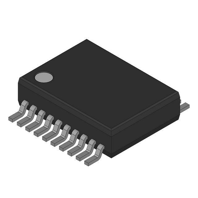
PLL1700
PLL
170
0
®
49%
FPO
SBOS096A – JANUARY 1998 – REVISED MAY 2007
MULTI-CLOCK GENERATOR
FEATURES
DESCRIPTION
● 27MHz MASTER CLOCK INPUT
The PLL1700 is a low cost, multi-clock generator Phase
Lock Loop (PLL).
● GENERATED AUDIO SYSTEM CLOCK:
SCKO1: 33.8688MHz (Fixed)
SCKO2: 256fS
SCKO3: 384fS
SCKO4: 768fS
The PLL1700 can generate four systems clocks from a
27MHz reference input frequency.
The device gives customers both cost and space savings
by eliminating external components and enables customers to achieve the very low jitter performance needed for
high-performance audio digital-to-analog converters
(DACs) and/or analog-to-digital converters (ADCs).
● ZERO PPM ERROR OUTPUT CLOCKS
● LOW CLOCK JITTER: 150ps at SCKO3
● MULTIPLE SAMPLING FREQUENCIES:
fS = 32kHz, 44.1kHz, 48kHz, 64kHz,
88.2kHz, 96kHz
The PLL1700 is ideal for MPEG-2 applications that use a
27MHz master clock such as DVD players, DVD add-on
cards for multimedia PCs, digital HDTV systems, and settop boxes.
● +3.3V CMOS LOGIC INTERFACE
● DUAL POWER SUPPLIES: +5V and +3.3V
● SMALL PACKAGE: 20-Lead SSOP
MODE
ML
MC
MD
VDDP GNDP VDDB GNDB VDD
Power Supply
Mode
Control
I/F
RST
GND
Reset
PLL2
XT1
OSC
PLL1
XT2
MCKO MCKO
SCKO1
Counter Q
Counter P
SCKO2
SCKO3
SCKO4
Please be aware that an important notice concerning availability, standard warranty, and use in critical applications of
Texas Instruments semiconductor products and disclaimers thereto appears at the end of this data sheet.
All trademarks are the property of their respective owners.
Copyright © 1998-2007, Texas Instruments Incorporated
PRODUCTION DATA information is current as of publication date.
Products conform to specifications per the terms of Texas Instruments
standard warranty. Production processing does not necessarily include
testing of all parameters.
www.ti.com
�ELECTROSTATIC
DISCHARGE SENSITIVITY
PIN CONFIGURATION
TOP VIEW
This integrated circuit can be damaged by ESD. Texas
Instruments recommends that all integrated circuits be
handled with appropriate precautions. Failure to observe proper handling and installation procedures can
cause damage.
ESD damage can range from subtle performance degradation to complete device failure. Precision integrated
circuits may be more susceptible to damage because
very small parametric changes could cause the device
not to meet its published specifications.
SSOP
ML/SR0
1
20
MC/FS1
MODE
2
19
MD/FS0
VDD
3
18
RST
GND
4
17
SCKO3
XT2
5
16
VDDB
PLL1700E
XT1
6
15
GNDB
GNDP
7
14
SCKO2
VDDP
8
13
SCKO4
RSV
9
12
SCKO1
MCKO 10
11
MCKO
(1)
ABSOLUTE MAXIMUM RATINGS
Supply Voltage (+VDD, +VDDP, +VDDB) .............................................. +6.5V
Supply Voltage Differences (+VDD, +VDDP) ....................................... ±0.1V
GND Voltage Differences: GND, GNDP, GNDB ............................... ±0.1V
Digital Input Voltage ................................................. –0.3V to (VDD + 0.3V)
Digital Output Voltage ............................................ –0.3V to (VDDB + 0.3V)
Input Current (any pins except supply pins) ................................... ±10mA
Power Dissipation .......................................................................... 300mW
Operating Temperature Range ......................................... –25°C to +85°C
Storage Temperature ...................................................... –55°C to +125°C
Lead Temperature (soldering, 5s) .................................................. +260°C
Package Temperature (IR reflow, 10s) .......................................... +235°C
NOTE: (1) Stresses above those listed under Absolute Maximum Ratings may
cause permanent damage to the device. Exposure to absolute maximum
conditions for extended periods may affect device reliability.
PIN ASSIGNMENTS
PIN
NAME
I/O
FUNCTION
1
ML/SR0
IN
Latch Enable for Software Mode/Sampling Rate
Selection for Hardware Mode. When MODE pin
is LOW, ML is selected.(1)
2
MODE
IN
Mode Control Select. When this pin is HIGH,
device is operated in hardware mode using SR0
(pin 1), FS0 (pin 19), and FS1 (pin 20). When
this pin is LOW, device is operated in software
mode by three-wire interface using ML (pin 1),
MD (pin 19) and MC (pin 20).(1)
3
VDD
—
Digital Power Supply, +5V.
4
GND
—
Digital Ground.
5
XT2
—
27MHz Crystal. When an external 27MHz clock
is applied to XT1 (pin 6), this pin must be
connected to GND.
6
XT1
IN
27MHz Oscillator Input/External 27MHz Input.
7
GNDP
—
Ground for PLL.
8
VDDP
—
Power Supply for PLL, +5V.
9
RSV
—
Reserved. Must be left open.
PACKAGE INFORMATION(1)
PRODUCT
PLL1700E
PACKAGE
20-Lead SSOP
SPECIFIED
TEMPERATURE
RANGE
–25°C to +85°C
PACKAGE
DESIGNATOR
DB
NOTE: (1) For the most current package and ordering information, see the
Package Option Addendum at the end of this data sheet, or see the TI web
site at www.ti.com.
10
MCKO
OUT
27MHz Output.
11
MCKO
OUT
Inverted 27MHz Output.
12
SCKO1
OUT
Fixed 33.8688MHz Clock Output.
13
SCKO4
OUT
768fS Clock Output.
14
SCKO2
OUT
256fS Clock Output.
15
GNDB
—
Digital Ground for VDDB.
16
VDDB
—
Digital Power Supply for Clock Output Buffers,
+3.3V.
17
SCKO3
OUT
384fS Output. This output has been optimized
for the lowest jitter and should be connected to
the audio DAC(s).
18
RST
IN
Reset. When this pin is LOW, device is held in
reset.(1)
19
MD/FS0
IN
Serial Data Input for Software Mode/Sampling
Frequency Selection for Hardware Mode. When
MODE pin is LOW, MD is selected.(1)
20
MC/FS1
IN
Shift Clock Input for Software Mode/Sampling
Frequency Selection for Hardware Mode. When
MODE pin is LOW, MC is selected.(1)
NOTE: (1) Schmitt-trigger input with internal pull-down resistors.
2
PLL1700
www.ti.com
SBOS096A
�ELECTRICAL CHARACTERISTICS
All specifications at TA = +25°C, VDD = VDDP = +5V, VDDB = +3.3V, fM = 27MHz crystal oscillation, and fS = 48kHz, unless otherwise noted.
PLL1700E
PARAMETER
DIGITAL INPUT/OUTPUT
Input Logic Level:
VIH(1)
VIL(1)
VIH(2)
VIL(2)
Input Logic Current:
IIH(1)
IIL(1)
IIH(2)
IIL(2)
Output Logic Level:
VOH(3)
VOL(3)
Sampling Frequency (fS)
CONDITIONS
VIN = VDD
VIN = 0V
VIN = VDD
VIN = 0V
200
–1
4
–800
µA
µA
mA
µA
0.4
48
96
VDC
VDC
kHz
kHz
CMOS
IOH = 4mA
IOL = 4mA
Standard fS
Double fS
C1 = C2 = 15pF
Fixed
256fS
384fS
768fS
20% to 80% VDDB
80% to 20% VDDB
SCKO1, SCKO3, SCKO4
SCKO2 (standard)
SCKO2 (double)(5)
SCKO1, SCKO2 (standard), SCKO4
SCKO3
SCKO2 (double)
To Programmed Frequency
To Programmed Frequency
VDD, VDDP
VDDB
VDDB – 0.4V
32
64
44.1
88.2
26.73
27
300
50
50
40
60
40
40
27.27
60
60
33.8688
40
40
25
+4.5
+2.7
MHz
ps
%
%
%
%
15
20
30
MHz
MHz
MHz
MHz
ns
ns
%
%
%
ps
ps
ps
ms
ms
+5
+3.3
+5.5
+3.6
VDC
VDC
11
6
75
16
9
110
mA
mA
mW
+85
+125
°C
°C
8.192
12.288
24.576
VDD = VDDP = 5V, fS = 48kHz
VDDB = +3.3V, fS = 48kHz
fS = 48kHz
TEMPERATURE RANGE
Operation
Storage
NOTES: (1)
(2)
(3)
(4)
(5)
(6)
0.4
1.2
fM = 27MHz, CL = 20pF
Supply Current(6):
IDD + IDDP
IDDB
Power Dissipation
UNITS
VDC
VDC
VDC
VDC
0.8
PHASE LOCK LOOP (PLL)
Generated System Clock Frequency
SCKO1
SCKO2
SCKO3
SCKO4
Generated Clock Rise Time(3)
Generated Clock Fall Time(3)
Generated Clock Duty Cycle
POWER SUPPLY REQUIREMENTS
Voltage Range
MAX
TTL-Compatible
fM = 27MHz, CL = 20pF
Settling Time
Power-Up Time
TYP
2.0
MASTER CLOCK (MCKO, MCKO)
Master Clock Frequency
Clock Jitter(4)
Clock Duty Cycle
MCKO
For Crystal Oscillation MCKO
Clock Duty Cycle
MCKO
For External Clock
MCKO
Generated Clock Jitter(4)
MIN
24.576
36.864
36.864
5
5
50
50
33
300
150
450
–25
–55
60
60
40
ML, MC, MD, MODE, RST (Schmitt-trigger input with internal pull-down resistor).
XT1, when an external 27MHz clock is used, the buffer ICs, such as 74HC04, are recommended to interface to XT1.
MCKO, MCKO, SCKO4, SCKO3, SCKO2, and SCKO1.
Jitter performance is specified as standard deviation of jitter under 27MHz crystal oscillation.
When SCKO2 is set to double rate clock output, its duty cycle is 33%.
fM = 27MHz crystal oscillation, no load on MCKO, MCKO, SCKO4, SCKO3, SCKO2, and SCKO1.
PLL1700
SBOS096A
www.ti.com
3
�TYPICAL CHARACTERISTICS
At TA = +25°C, VDD = VDDP = +5V, VDDB = +3.3V, CL = 20pF, unless otherwise noted.
JITTER vs SAMPLING FREQUENCY
SCKO3 JITTER vs TEMPERATURE
400
300
Jitter (pS rms)
SCKO Jitter (pS rms)
SCKO1
300
200
MCKO
100
32kHz
200
96kHz
100
48kHz
SCKO3
0
0
32
44.1
48
96
–25
+25
Sampling Frequency, fS (kHz)
DUTY CYCLE RATIO vs SAMPLING FREQUENCY
SCKO3 JITTER vs VDDB
300
32kHz
60
SCKO3
SCKO Jitter (pS rms)
Duty Cycle Ratio (%)
70
MCKO (XTAL Operation)
50
MCKO (External Clock)
40
30
200
96kHz
48kHz
100
0
32
44.1
48
96
2.7
Sampling Frequency, fS (kHz)
4
+85
Temperature (°C)
3.3
3.6
VDDB (V)
PLL1700
www.ti.com
SBOS096A
�THEORY OF OPERATION
oscillator placed between XT1 (pin 6) and XT2 (pin 5), or
an external input to XT1. If an external master clock is
used, XT2 must be connected to ground. In both cases,
the signal amplitude on XT1 must satisfy the specification
described in Figure 3. Therefore, careful C1 and C2
determination is required for keeping this specification
when using a crystal oscillator.
Figure 2 illustrates possible system clock connection
options. Figure 3 illustrates the 27MHz master clock
timing requirements.
MASTER CLOCK AND SYSTEM CLOCK OUTPUT
The PLL1700 consists of a dual PLL clock and master
clock generator which generates four system clocks and
two buffered 27MHz clocks from a 27MHz master clock.
Figure 1 shows the block diagram of the PLL1700. The
PLL is designed to accept a 27MHz master clock or
crystal oscillator. The master clock can be either a crystal
SCKO2
256fS
Frequency Control
PLL2
Counter N
Data
ROM
Counter M
Phase Detector
and
Loop Filter
VCO
Counter Q
PLL1
Counter M
OSC
Counter N
XT2
XT1
Phase Detector
and
Loop Filter
Counter P
VCO
SCKO1
33.8688MHz
MCKO MCKO
27MHz
SCKO4
768fS
SCKO3
384fS
FIGURE 1. Block Diagram of PLL1700.
MCKO
MCKO
Buffer
Buffer
MCKO
MCKO
Buffer
C1
Xtal
C2
Buffer
XTI
XT2
C1, C2 = 10pF to 33pF
Crystal
OSC
Circuit
27MHz Internal
Master Clock
External Clock
XT1
XT2
PLL1700
27MHz Internal
Master Clock
Crystal
OSC
Circuit
PLL1700
Crystal Resonator Connection
External Clock Input
FIGURE 2. Master Clock Generator Connection Diagram.
tXT1H
1.2V
DESCRIPTION
0.4V
XT1
SYMBOL
MIN
TYP
MAX
UNITS
System Clock Pulse Width HIGH
tXT1H
10
ns
System Clock Pulse Width LOW
tXT1L
15
ns
tXT1L
FIGURE 3. External Master Clock Timing Requirement.
PLL1700
SBOS096A
www.ti.com
5
�The PLL1700 provides a very low jitter, high accuracy
clock. SCKO1 is a fixed frequency clock which is
33.8688MHz (768 x 44.1kHz) for a CD-DA DSP. The
output frequency of the remaining clocks is determined by
the sampling frequency (fS) by software or hardware
control. SCKO2 and SCKO3 output 256fS and 384fS
systems clocks, respectively. SCKO4 output is 768fS if the
sampling frequency is 32kHz, 44.1kHz, 48kHz, or the
output is 384fS if the sampling frequency is 64kHz, 88.2kHz,
or 96kHz. Table I shows each sampling frequency. The
system clock output frequencies are generated by a
27MHz master clock and programmed sampling frequencies are shown in Table II.
SAMPLING
FREQUENCY (kHz)
SAMPLING RATE
Standard Sampling Frequencies
32
44.1
48
Double of Standard Sampling Frequencies
64
88.2
96
FUNCTION CONTROL
The built-in function of the PLL1700 can be controlled in
the software mode (serial mode), which uses a three-wire
interface by ML (pin 1), MC (pin 20), and MD (pin 19), when
MODE (pin 2) = L. They can also be controlled in the
hardware mode (parallel mode) which uses SR0 (pin 1),
FS1 (pin 20) and FS0 (pin 19), when MODE (pin 2) = H.
The selectable functions are shown in Table III.
HARDWARE
MODE
(MODE = H)
SOFTWARE
MODE
(MODE = L)
Sampling Frequency Select
(32kHz, 44.1kHz, 48kHz)
Yes
Yes
Sampling Rate Select (Standard/Double)
Yes
Yes
Each Clock Output Enable/Disable
No
Yes
FUNCTION
TABLE III. Selectable Functions.
TABLE I. Sampling Frequencies.
HARDWARE MODE (MODE = H)
In the hardware mode, the following functions can be
selected:
SAMPLING
FREQUENCY
(kHz)
SAMPLING
RATE
SKCO2
(MHz)
SCKO3
(MHz)
SCKO4
(MHz)
32
Standard
8.192
12.288
24.576
44.1
Standard
11.2896
16.9344
33.8688
48
Standard
12.288
18.4320
36.8640
Sampling Group Select
64
Double
16.384
24.576
24.576
88.2
Double
22.5792
33.8688
33.8688
96
Double
24.576
36.8640
36.8640
The sampling frequency group can be selected by FS1
(pin 20) and FS0 (pin 19). This selection must be made
with an interval time greater than 20µs.
FS1 (Pin 20)
TABLE II. Sampling Frequencies and Master Clock
Output Frequencies.
Response time from power-on (or applying the clock to
XT1) to SCKO settling time is typically 15ms. Delay time
from sampling frequency change to SCKO settling time is
20ms maximum. Figure 4 illustrates SCKO transient
timing.
External buffers are recommended on all output clocks in
order to avoid degrading the jitter performance of the
PLL1700.
SAMPLING GROUP
L
L
48kHz
L
H
44.1kHz
H
L
32kHz
H
H
Reserved
Sampling Rate Select
The sampling rate can be selected by SR0 (pin 1).
SR0 (Pin 1)
SAMPLING RATE SELECT
L
Standard
H
Double
SOFTWARE MODE (MODE = L)
RESET
The PLL1700 has an internal power-on reset circuit, as
well as an external forced reset (RST, pin 18). Both resets
have the same effect on the PLL1700 functions. The
mode register default settings for software mode are
initialized by reset. Throughout the reset period, all clock
outputs are enabled with the default settings. Initialization
for the internal power-on reset is done automatically
during 1024 master clocks at VDD ≥ 2.2V (1.8V to 2.6V).
When using the internal power-on reset, RST should be
HIGH. Power-on reset timing is shown in Figure 5. RST
(pin 18) accepts an external forced reset by RST = L.
Initialization (reset) is done when RST = L and 1024
master clocks after RST = H. External reset timing is
shown in Figures 6 and 7.
6
FS0 (Pin 19)
The PLL1700 special function in software mode is shown
in Table IV. These functions are controlled using ML, MC,
and MD serial control signal.
FUNCTION
Sampling Frequency Select (32kHz, 44.1kHz, 48kHz)
Sampling Rate Select (Standard/Double)
Each Clock Output Enable/Disable
DEFAULT
48kHz Group
Standard
Enable
TABLE IV. Selectable Functions.
PLL1700
www.ti.com
SBOS096A
�ML
20ms
3 clocks of MCKO
SCKO2
SCKO3
SCKO4
Stable
Clock Transistion Region
Stable
33.8688MHz
SCKO1
FIGURE 4. System Clock Transient Timing Chart.
VDD
2.6V
2.2V
1.8V
Reset
Reset Removal
Internal Reset
1024 System Clock Periods
Master Clock
FIGURE 5. Power-On Reset Timing.
RST
tRST
Reset
Reset Removal
Internal Reset
1024 System Clock Periods
Master Clock
FIGURE 6. External Reset Timing.
RST
1.4V
tRST
System Clock Pulse Width LOW
tRST
20ns
(min)
FIGURE 7. Reset Pulse Timing Requirement.
PLL1700
SBOS096A
www.ti.com
7
�PROGRAM REGISTER BIT-MAPPING
Mode Register
The built-in functions of the PLL1700 are controlled through
a 16-bit program register. This register is loaded using
MD. After the 16 data bits are clocked in using the rising
edge of MC, ML is used to latch the data into the register.
Table V shows the bit-mapping of the registers. The
software mode control format and control data input
timing is shown in Figures 8 and 9, respectively.
FS [1:0]:
Sampling Frequency Group Select. This selection must be made with an interval time
greater than 20µs.
FS1
FS0
SAMPLING FREQUENCY
DEFAULT
0
0
1
1
0
1
0
1
48kHz
44.1kHz
32kHz
Reserved
O
Mode Register
D15 D14 D13 D12 D11 D0 D9
0
1
1
REGISTER
MODE
1
0
D8
D7
D6
D5
D4
D3
D2
D1
D0
SR [1:0]:
0 CE6 CE5 CE4 CE3 CE2 CE1 SR1 SR0 FS1 FS0
BIT NAME
CE6
CE5
CE4
CE3
CE2
CE1
SR [1:0]
FS [1:0]
SR1
SR0
SAMPLING RATE
DEFAULT
0
0
1
1
0
1
0
1
Standard
Double
Reserved
Reserved
O
DESCRIPTION
MCKO Output Enable/Disable
MCKO Output Enable/Disable
SCKO4 Output Enable/Disable
SCKO3 Output Enable/Disable
SCKO2 Output Enable/Disable
SCKO1 Output Enable/Disable
Sampling Rate Select
Sampling Frequency Select
Sample Rate Select
CE [1:6]:
TABLE V. Register Mapping.
Clock Output Control
CE1 - CE6
CLOCK OUTPUT CONTROL
DEFAULT
0
1
Clock Output Disable
Clock Output Enable
O
ML (pin 1)
MC (pin 20)
MD (pin 19) D15 D14 D13 D12 D11 D10 D9 D8 D7 D6 D5 D4 D3 D2 D1 D0
FIGURE 8. Software Mode Control Format.
tMLL
tMHH
ML (pin 1)
1.4V
tMLS
tMCH
tMCL
tMLH
tMLS
1.4V
MC (pin 20)
tMCY
MD (pin 19)
1.4V
MSB
LSB
tMDS
DESCRIPTION
MC Pulse Cycle Time
MC Pulse Width LOW
MC Pulse Width HIGH
MD Hold Time
MD Set-Up Time
ML Low Level Time
ML High Level Time
ML Hold Time(2)
ML Set-Up Time(3)
tMDH
SYMBOL
MIN
tMCY
tMCL
tMCH
tMDH
tMDS
tMLL
tMHH
tMLH
tMLS
100
40
40
40
40
16
200
40
40
TYP
MAX
UNITS
ns
ns
ns
ns
ns
MC Clocks(1)
ns
ns
ns
NOTES: (1) MC clocks: MC clock period. (2) MC rising edge for LSB to ML rising edge. (3) ML rising edge
to the next MC rising edge. If the MC Clock is stopped after the LSB, any ML rising time is accepted.
FIGURE 9. Control Data Input Timing.
8
PLL1700
www.ti.com
SBOS096A
�CONNECTION DIAGRAM
MPEG-2 APPLICATIONS
Figure 10 shows the typical connection circuit for the
PLL1700. There are three grounds for digital, analog and
PLL power supply. However, the use of one common
ground connection is recommended to avoid latch-up
problems. Power supplies should be bypassed as close
as possible to the device.
Typical applications for the PLL1700 are MPEG-2 based
systems such as DVD players, DVD add-on cards for
multimedia PCs, digital HDTV systems, and set-top boxes.
The PLL1700 provides audio system clocks for a CD-DA
DSP, DVD DSP, Karaoke DSP, and DAC(s) from a
27MHz video clock.
+
C1
22µF to 47µF
C2
+
+5V
+3.3 V
22µF to 47µF
PLL1700E
1
ML/SR01
MC/FS1 20
2
MODE
MD/FS0 19
3
VDD
4
GND
5
XT2
VDDB 16
6
XT1
GNDB 15
7
GNDP
SCKO2 14
8
VDDP
SCKO4 13
9
RSV
SCKO1 12
0.1µF and 10µF(1)
C3
(2)
C4
0.1µF
and
10µF(1)
10 MCKO
Mode
Control
RST 18
SCKO3 17
C5
0.1µF
and
10µF(1)
Clock
Output(3)
MCKO 11
NOTES: (1) 0.1µF ceramic and 10µF electrolytic capacitor typical, depending on quality of power supply and pattern layout.
(2) 27MHz quartz crystal and 10pF through two 33pF ceramic capacitors.
(3) To achieve best possible jitter performance, it is recommended to minimize the load capacitance on the clock output.
FIGURE 10. Typical Connection Diagram.
PLL1700
SCKO3
SCKO4
27MHz
Crystal
SCKO2
MCKO
384fS
768fS
256fS
PCM1716
Front
PCM1716
Surround
27MHz
SCKO1
CD-DA/
DVD DSP
MPEG/AC-3
Audio Decoder
Karaoke
DSP
PCM1716
Center
Subwoofer
FIGURE 11. PLL1700 System Application Block Diagram.
PLL1700
SBOS096A
www.ti.com
9
�Revision History
DATE
5/07
REVISION
PAGE
SECTION
—
Entire Document
3
Electrical Characteristics
5
Master Clock and
System Clock Output
5
Figure 5
6
Sampling Group Select
Added text regarding interval time.
8
Mode Register
Added text regarding interval time.
9
Figure 10
A
DESCRIPTION
Updated format to current standard look.
Added note (1) to VIH and VIL.
Added two rows to Input Logic Level for VIH and VIL with note (2).
Added condition to Clock Duty Cycle row stating that C1 = C2 = 15pF.
Changed "X2 should be connected" to "X2 must be connected."
Added text regarding signal amplitude.
Changed voltage from 2.0V to 1.2V.
Changed voltage from 0.8V to 0.4V.
Changed tXT1H min value from 15 to 10.
Deleted note (1) from C1 and C2.
Changed note text from "tantalum" to "electrolytic" capacitor.
NOTE: Page numbers for previous revisions may differ from page numbers in the current version.
10
PLL1700
www.ti.com
SBOS096A
�PACKAGE OPTION ADDENDUM
www.ti.com
14-Oct-2022
PACKAGING INFORMATION
Orderable Device
Status
(1)
Package Type Package Pins Package
Drawing
Qty
Eco Plan
(2)
Lead finish/
Ball material
MSL Peak Temp
Op Temp (°C)
Device Marking
(3)
(4/5)
(6)
PLL1700E
NRND
SSOP
DB
20
65
RoHS & Green
NIPDAU
Level-1-260C-UNLIM
PLL1700E
PLL1700E/2K
NRND
SSOP
DB
20
2000
RoHS & Green
NIPDAU
Level-1-260C-UNLIM
PLL1700E
PLL1700EG
NRND
SSOP
DB
20
65
RoHS &
Non-Green
SNBI
Level-1-260C-UNLIM
PLL1700EG
PLL1700EG/2K
NRND
SSOP
DB
20
2000
RoHS &
Non-Green
SNBI
Level-1-260C-UNLIM
PLL1700EG
(1)
The marketing status values are defined as follows:
ACTIVE: Product device recommended for new designs.
LIFEBUY: TI has announced that the device will be discontinued, and a lifetime-buy period is in effect.
NRND: Not recommended for new designs. Device is in production to support existing customers, but TI does not recommend using this part in a new design.
PREVIEW: Device has been announced but is not in production. Samples may or may not be available.
OBSOLETE: TI has discontinued the production of the device.
(2)
RoHS: TI defines "RoHS" to mean semiconductor products that are compliant with the current EU RoHS requirements for all 10 RoHS substances, including the requirement that RoHS substance
do not exceed 0.1% by weight in homogeneous materials. Where designed to be soldered at high temperatures, "RoHS" products are suitable for use in specified lead-free processes. TI may
reference these types of products as "Pb-Free".
RoHS Exempt: TI defines "RoHS Exempt" to mean products that contain lead but are compliant with EU RoHS pursuant to a specific EU RoHS exemption.
Green: TI defines "Green" to mean the content of Chlorine (Cl) and Bromine (Br) based flame retardants meet JS709B low halogen requirements of