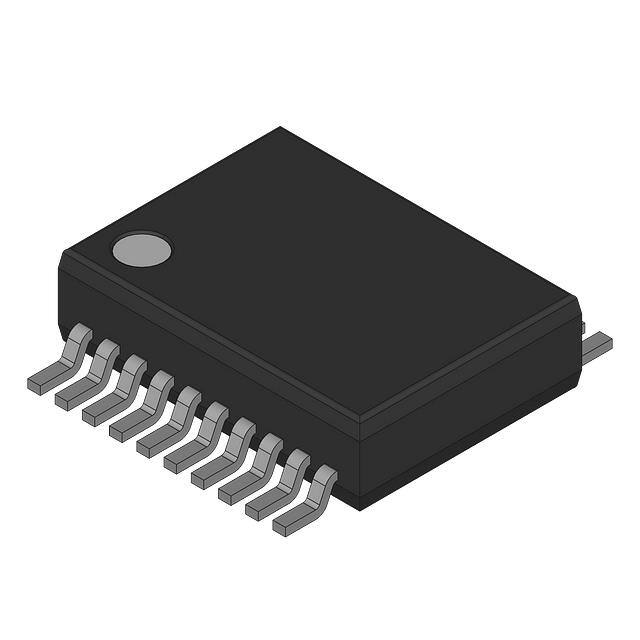
PLL1707-Q1
SLES259A – JUNE 2010 – REVISED MARCH 2011
www.ti.com
3.3-V DUAL-PLL MULTICLOCK GENERATOR
Check for Samples: PLL1707-Q1
FEATURES
1
•
•
•
•
•
•
Qualified for Automotive Applications
27-MHz Master Clock Input
Generated Audio System Clock
– SCKO0: 768 fS (fS = 44.1 kHz)
– SCKO1: 768 fS, 512 fS (fS = 48 kHz)
– SCKO2: 256 fS (fS = 32, 44.1, 48, 64, 88.2, 96
kHz)
– SCKO3: 384 fS (fS = 32, 44.1, 48, 64, 88.2, 96
kHz)
Zero PPM Error Output Clocks
Low Clock Jitter: 50 ps (Typical)
Multiple Sampling Frequencies:
fS = 32, 44.1, 48, 64, 88.2, 96 kHz
•
•
•
3.3-V Single Power Supply
Parallel Control
Package: 20-Pin SSOP (150 mil), Lead-Free
Product
APPLICATIONS
•
•
•
•
•
•
•
HDD + DVD Recorders
DVD Recorders
HDD Recorders
DVD Players
DVD Add-On Cards for Multimedia PCs
Digital HDTV Systems
Set-Top Boxes
DESCRIPTION
The PLL1707 is a low-cost phase-locked loop (PLL) multiclock generator. The PLL1707 can generate four
system clocks from a 27-MHz reference input frequency. The clock outputs of the PLL1707 can be controlled by
sampling frequency-control pins. The device gives customers both cost and space savings by eliminating
external components and enables customers to achieve the very low-jitter performance needed for high
performance audio DACs and/or ADCs. The PLL1707 is ideal for MPEG-2 applications that use a 27-MHz
master clock such as DVD recorders, HDD recorders, DVD add-on cards for multimedia PCs, digital HDTV
systems, and set-top boxes.
FUNCTIONAL BLOCK DIAGRAM
SR
FS2
FS1
CSEL
Mode Control Interface
VCC AGND VDD1–3 DGND1–3
Power Supply
Reset
PLL2
XT1
OSC
PLL1
XT2
MCKO1
MCKO2
SCKO0
Divider
Divider
Divider
SCKO1
SCKO2
SCKO3
1
Please be aware that an important notice concerning availability, standard warranty, and use in critical applications of Texas
Instruments semiconductor products and disclaimers thereto appears at the end of this data sheet.
PRODUCTION DATA information is current as of publication date.
Products conform to specifications per the terms of the Texas
Instruments standard warranty. Production processing does not
necessarily include testing of all parameters.
Copyright © 2010–2011, Texas Instruments Incorporated
�PLL1707-Q1
SLES259A – JUNE 2010 – REVISED MARCH 2011
www.ti.com
This integrated circuit can be damaged by ESD. Texas Instruments recommends that all integrated circuits be handled with
appropriate precautions. Failure to observe proper handling and installation procedures can cause damage.
ESD damage can range from subtle performance degradation to complete device failure. Precision integrated circuits may be more
susceptible to damage because very small parametric changes could cause the device not to meet its published specifications.
ORDERING INFORMATION (1)
PACKAGE (2)
TA
-40°C to 85°C
(1)
(2)
SSOP - DBQ
ORDERABLE PART NUMBER
Reel of 2500
PLL1707IDBQRQ1
TOP-SIDE MARKING
PLL1707I
For the most current package and ordering information, see the Package Option Addendum at the end of this document, or see the TI
web site at www.ti.com.
Package drawings, thermal data, and symbolization are available at www.ti.com/packaging.
ABSOLUTE MAXIMUM RATINGS (1)
over operating free-air temperature range (unless otherwise noted)
VCC
Supply voltage: VDD1-VDD3
ΔVCC
Supply voltage differences: VDD1-VDD3
4V
±0.1 V
±0.1 V
Ground voltage differences: AGND, DGND1-DGND3
VI
Digital input voltage: FS1, FS2, SR, CSEL
-0.3 V to (VDD + 0.3) V
VI
Analog input voltage, XT1, XT2
-0.3 V to (VCC + 0.3) V
II
Input current (any pins except supplies)
TA
Ambient temperature range
-40°C to 85°C
Tstg
Storage temperature
-55°C to 150°C
TJ
Junction temperature
150°C
(1)
±10 mA
Stresses beyond those listed under absolute maximum ratings may cause permanent damage to the device. These are stress ratings
only and functional operation of the device at these or any other conditions beyond those indicated under recommended operating
conditions is not implied. Exposure to absolute-maximum-rated conditions for extended periods may affect device reliability.
ELECTRICAL CHARACTERISTICS
TA = 25°C, VDD1-VDD3 (= VDD) = VCC = 3.3 V, fM = 27 MHz, crystal oscillation, fS = 48 kHz (unless otherwise noted)
PARAMETER
TEST CONDITIONS
MIN
TYP
MAX
UNIT
DIGITAL INPUT/OUTPUT
Logic input
VIH
VIL
IIH
IIL
CMOS compatible
0.7 VDD
Input logic level (1)
Input logic current (1)
VIN = VDD
65
VOL
Output logic level (2) (3)
Sampling frequency
(1)
(2)
(3)
2
100
±10
VIN = 0 V
Logic output
VOH
3.6
0.3 VDD
Vdc
µA
CMOS
IOH = -4 mA
VDD - 0.4
Vdc
IOL = 4 mA
0.4
Standard fS
32
44.1
48
Double fS
64
88.2
96
Vdc
kHz
Pins 5, 6, 7, 12: FS1, FS2, SR, CSEL (Schmitt-trigger input with internal pulldown, 3.3-V tolerant)
Pins 2, 3, 14, 15, 18, 19: SCKO2, SCKO3, MCKO1, MCKO2, SCKO0, SCKO1
Not production tested
Submit Documentation Feedback
Copyright © 2010–2011, Texas Instruments Incorporated
Product Folder Link(s): PLL1707-Q1
�PLL1707-Q1
SLES259A – JUNE 2010 – REVISED MARCH 2011
www.ti.com
ELECTRICAL CHARACTERISTICS (continued)
TA = 25°C, VDD1-VDD3 (= VDD) = VCC = 3.3 V, fM = 27 MHz, crystal oscillation, fS = 48 kHz (unless otherwise noted)
PARAMETER
TEST CONDITIONS
MIN
TYP
MAX
UNIT
27
27.27
MHz
MASTER CLOCK (MCKO1, MCKO2) (fM = 27 MHz, C1 = C2 = 15 pF, CL = 20 pF on measurement pin)
Master clock frequency
VIH
VIL
IIH
IIL
26.73
0.7 VCC
Input level (4) (5)
Input current (4)
VIN = VCC
±10
VIN = 0 V
±10
Output voltage (6)
3.5
Output rise time
20% to 80% of VDD
2
Output fall time
80% to 20% of VDD
2
For crystal oscillation
Duty cycle
V
0.3 VCC
45
For external clock
51
µA
Vp-p
ns
ns
55 %
50
Clock jitter (7)
50
Power-up time (8)
0.5
ps
1.5
ms
PLL AC CHARACTERISTICS (SCKO0-SCKO3) (fM = 27 MHz, CL = 20 pF on measurement pin)
SCKO0
Fixed
SCKO1
Selectable for 48 kHz
SCKO2
Output system clock frequency (9)
SCKO3
33.8688
24.576
36.864
256 fS
8.192
12.288
24.576
384 fS
12.288
18.432
36.864
MHz
Output rise time
20% to 80% of VDD
2
ns
Output fall time
80% to 20% of VDD
2
ns
Output duty cycle
Output clock jitter (7) (5)
Frequency settling time (10)
Power-up time
(11)
50
55
%
SCKO0, SCKO1
45
58
100
ps
SCKO2, SCKO3
50
100
ps
To stated output frequency
50
150
ns
To stated output frequency
3
6
ms
3.3
3.6
POWER SUPPLY
VCC, VDD
IDD + ICC
Supply voltage
2.7
V
(12)
VDD = VCC = 3.3 V, fS = 48 kHz
19
35
mA
Power dissipation
VDD = VCC = 3.3 V, fS = 48 kHz
63
130
mW
Supply current
TEMPERATURE
Operating temperature
θJA
-40
Thermal resistance
85
150
°C
°C/W
(4)
(5)
(6)
(7)
Pin 10: XT1
Not production tested
Pin 11: XT2
Jitter performance is specified as standard deviation of jitter for 27-MHz crystal oscillation and default SCKO frequency setting. Jitter
performance varies with master clock mode, SCKO frequency setting and load capacitance on each clock output.
(8) The delay time from power on to oscillation
(9) The MIN and MAX values are the low and high selectable frequencies based on frequency (fS) selected (see Table 2 through Table 4)
(10) The settling time when the sampling frequency is changed
(11) The delay time from power on to lockup
(12) fM = 27-MHz crystal oscillation, no load on MCKO1, MCKO2, SCKO0, SCKO1, SCKO2, SCKO3. Power supply current varies with
sampling frequency selection and load condition.
Submit Documentation Feedback
Copyright © 2010–2011, Texas Instruments Incorporated
Product Folder Link(s): PLL1707-Q1
3
�PLL1707-Q1
SLES259A – JUNE 2010 – REVISED MARCH 2011
www.ti.com
DBQ PACKAGE
(TOP VIEW)
VDD1
SCKO2
SCKO3
DGND1
FS1
FS2
SR
VCC
AGND
XT1
1
2
3
4
5
6
7
8
9
10
20
19
18
17
16
15
14
13
12
11
VDD3
SCKO1
SCKO0
DGND3
DGND2
MCKO2
MCKO1
VDD2
CSEL
XT2
TERMINAL FUNCTIONS
TERMINAL
NAME
4
NO.
I/O
DESCRIPTION
AGND
9
-
Analog ground
CSEL
12
I
SCKO1 frequency selection control(1)
DGND1
4
-
Digital ground 1
DGND2
16
-
Digital ground 2
DGND3
17
-
Digital ground 3
FS1
5
I
Sampling frequency group control 1(1)
FS2
6
I
Sampling frequency group control 2(1)
MCKO1
14
O
27-MHz master clock output 1
MCKO2
15
O
27-MHz master clock output 2
SCKO0
18
O
System clock output 0 (33.8688 MHz fixed)
SCKO1
19
O
System clock output 1 (selectable for 48 kHz)
SCKO2
2
O
System clock output 2 (256 fS selectable)
SCKO3
3
O
System clock output 3 (384 fS selectable)
SR
7
I
Sampling rate control(1)
VCC
8
-
Analog power supply, 3.3 V
VDD1
1
-
Digital power supply 1, 3.3 V
VDD2
13
-
Digital power supply 2, 3.3 V
VDD3
20
-
Digital power supply 3, 3.3 V
XT1
10
I
27-MHz crystal oscillator, or external clock input
XT2
11
O
27-MHz crystal oscillator, must be OPEN for external clock input mode
Submit Documentation Feedback
Copyright © 2010–2011, Texas Instruments Incorporated
Product Folder Link(s): PLL1707-Q1
�PLL1707-Q1
SLES259A – JUNE 2010 – REVISED MARCH 2011
www.ti.com
TYPICAL PERFORMANCE CURVES
All specifications at TA = 25°C, VDD1-3 (= VDD) = VCC = +3.3 V, fM = 27 MHz, crystal oscillation, C1, C2 = 15 pF, default
frequency (33.8688 MHz for SCKO0, 36.864 MHz for SCKO1, 256 fS and 384 fS of 48 kHz for SCKO2 and SCKO3), CL = 20
pF on measurement pin, unless otherwise noted.
JITTER
vs
SAMPLING FREQUENCY
JITTER
vs
LOAD CAPACITANCE
70
70
65
MCKO1
SCKO0
SCKO2
MCKO2
SCKO1
SCKO3
65
SCKO1
SCKO0
60
Jitter − psrms
Jitter − psrms
60
55
SCKO3
55
SCKO2
50
50
45
45
MCKO2
MCKO1
40
40
30
40
50
60
70
80
90
100
0
5
f S − Sampling Frequency − kHz
10
Figure 1.
JITTER
vs
FREE-AIR TEMPERATURE
70
70
65
SCKO1
SCKO1
SCKO0
SCKO0
SCKO3
MCKO2
50
55
MCKO2
50
45
40
2.7
SCKO3
60
Jitter − psrms
Jitter − psrms
60
55
20
Figure 2.
JITTER
vs
SUPPLY VOLTAGE
65
15
CL − Load Capacitance − pF
3.0
45
MCKO1
SCKO2
3.3
3.6
40
−50
VCC − Supply Voltage − V
MCKO1
SCKO2
−25
0
25
50
75
100
TA − Free-Air Temperature − °C
Figure 3.
Figure 4.
Submit Documentation Feedback
Copyright © 2010–2011, Texas Instruments Incorporated
Product Folder Link(s): PLL1707-Q1
5
�PLL1707-Q1
SLES259A – JUNE 2010 – REVISED MARCH 2011
www.ti.com
TYPICAL PERFORMANCE CURVES (continued)
All specifications at TA = 25°C, VDD1-3 (= VDD) = VCC = +3.3 V, fM = 27 MHz, crystal oscillation, C1, C2 = 15 pF, default
frequency (33.8688 MHz for SCKO0, 36.864 MHz for SCKO1, 256 fS and 384 fS of 48 kHz for SCKO2 and SCKO3), CL = 20
pF on measurement pin, unless otherwise noted.
DUTY CYCLE
vs
SUPPLY VOLTAGE
DUTY CYCLE
vs
FREE-AIR TEMPERATURE
55
55
54
54
MCKO1
52
Duty Cycle − %
53
MCKO2
52
SCKO2
Duty Cycle − %
53
51
50
49
48
SCKO1
SCKO3
50
49
48
SCKO0
47
46
46
3.0
3.3
3.6
45
−50
VCC − Supply Voltage − V
SCKO0
−25
0
25
SCKO3
50
75
100
TA − Free-Air Temperature − °C
Figure 5.
6
SCKO2
51
47
45
2.7
MCKO2
SCKO1
MCKO1
Figure 6.
Submit Documentation Feedback
Copyright © 2010–2011, Texas Instruments Incorporated
Product Folder Link(s): PLL1707-Q1
�PLL1707-Q1
SLES259A – JUNE 2010 – REVISED MARCH 2011
www.ti.com
THEORY OF OPERATION
Master Clock and System Clock Output
The PLL1707 consists of a dual PLL clock and master clock generator which generates four system clocks and
two buffered 27-MHz clocks from a 27-MHz master clock. Figure 7 shows the block diagram of the PLL1707. The
PLL is designed to accept a 27-MHz master clock.
SCKO3
384 fS
Counter N
SCKO0−3
Frequency
Control
Phase Detector
and
Loop Filter
Divider
VCO
Counter M
Divider
PLL2
PLL1
Counter M
Phase Detector
and
Loop Filter
VCO
Counter N
OSC
XT1 XT2 MCKO1
27 MHz
Divider
MCKO2
27 MHz
SCKO0
33.8688 MHz
SCKO1
36.864/24.576 MHz
SCKO2
256 fS
Figure 7. Block Diagram
The master clock can be either a crystal oscillator placed between XT1 (pin 10) and XT2 (pin 11), or an external
input to XT1. If an external master clock is used, XT2 must be open. Figure 8 illustrates possible system clock
connection options, and Figure 9 illustrates the 27-MHz master clock timing requirement.
Submit Documentation Feedback
Copyright © 2010–2011, Texas Instruments Incorporated
Product Folder Link(s): PLL1707-Q1
7
�PLL1707-Q1
SLES259A – JUNE 2010 – REVISED MARCH 2011
www.ti.com
MCKO2
MCKO2
MCKO1
MCKO1
27-MHz
Internal
Master
Clock
XT1
C1
Crystal
Crystal
OSC
Circuit
XT1
External
Clock
Crystal
OSC
Circuit
XT2
27-MHz
Internal
Master
Clock
XT2
C2
PLL1707
PLL1707
C1, C2 = 10 pF to 33 pF
Crystal Resonator Connection
External Clock Input Connection
Figure 8. Master Clock Generator Connection Diagram
t (XT1H)
0.7 VCC
XT1
0.3 VCC
t (XT1L)
Figure 9. External Master Clock Timing Requirements
Table 1. External Master Clock Timing Requirements
DESCRIPTION
SYMBOL
MIN
Master clock pulse duration HIGH
t(XT1H)
10
MAX
UNIT
ns
Master clock pulse duration LOW
t(XT1L)
10
ns
The PLL1707 provides a very low-jitter high-accuracy clock. SCKO0 outputs a fixed 33.8688-MHz clock, SCKO1
outputs 512 fS or 768 fS (fS = 48 kHz), which is selected by hardware or software control (see Table 2). The
output frequency of the remaining clocks is determined by the sampling frequency (fS) under hardware or
software control. SCKO2 and SCKO3 output 256-fS and 384-fS system clocks, respectively. Table 3 shows each
sampling frequency which can be programmed. The system clock output frequencies for programmed sampling
frequencies are shown in Table 4.
Table 2. Generated System Clock SCKO1 Frequency
fS
SCKO1 FREQUENCY
512 fS
24.576 MHz
768 fS
36.864 MHz
Table 3. Sampling Frequencies
SAMPLING RATE
8
SAMPLING FREQUENCY (kHz)
Standard sampling frequencies
32
44.1
48
Double sampling frequencies
64
88.2
96
Submit Documentation Feedback
Copyright © 2010–2011, Texas Instruments Incorporated
Product Folder Link(s): PLL1707-Q1
�PLL1707-Q1
SLES259A – JUNE 2010 – REVISED MARCH 2011
www.ti.com
Table 4. Sampling Frequencies and System Clock Output Frequencies
SAMPLING
FREQUENCY (kHz)
SAMPLING RATE
256 fS SCKO2 (MHZ)
384 fS SCKO3 (MHZ)
32
Standard
8.192
12.288
44.1
Standard
11.2896
16.9344
48
Standard
12.288
18.432
64
Double
16.384
24.576
88.2
Double
22.5792
33.8688
96
Double
24.576
36.864
Response time from power on (or applying the clock to XT1) to SCKO settling time is typically 3 ms. Delay time
from sampling frequency change to SCKO settling is 300 ns maximum.
The delay time for hardware control to use SR, FS2, FS1, or CSEL is 150 ns maximum. Figure 10 illustrates
SCKO transient timing in the PLL1707. Clock transient timing is not synchronized with the SCKOs. External
buffers are recommended on all output clocks in order to avoid degrading the jitter performance of the PLL1707.
SR
FS2, 1
CSEL
150 ns
50 ns
SCKO1
SCKO2
SCKO3
Stable
Clock T ransition Region
SCKO0
Stable
33.8688 MHz
Figure 10. SCKO Transient Timing
Power-On Reset
The PLL1707 has an internal power-on reset circuit. Throughout the reset period, all clock outputs are enabled
with the default settings after power-up time. Initialization by internal power-on reset is done automatically during
1024 master clocks at VDD > 2.0 V (TYP). Power-on reset timing is shown in Figure 11.
VDD
2.4 V
2.0 V
1.6 V
Reset
Reset Removal
Internal Reset
1024 Master Clocks
Master Clock
Figure 11. Power-On Reset Timing
Submit Documentation Feedback
Copyright © 2010–2011, Texas Instruments Incorporated
Product Folder Link(s): PLL1707-Q1
9
�PLL1707-Q1
SLES259A – JUNE 2010 – REVISED MARCH 2011
www.ti.com
Functional Control
The built-in functions of the PLL1707 can be controlled in the parallel mode (hardware mode), which uses SR
(pin 7), FS1 (pin 5) and FS2 (pin 6). The selectable functions are shown in Table 5.
Table 5. Selectable Functions
SELECTABLE FUNCTION
PARALLEL MODE
Sampling frequency select (32 kHz, 44.1 kHz, 48 kHz)
Yes
Sampling rate select (standard/double)
Yes
PLL1707 (Parallel Mode)
In the parallel mode, the following functions can be selected:
Sampling Frequency Group Select
The sampling frequency group can be selected by FS1 (pin 5) and FS2 (pin 6).
Table 6. Sampling Frequency Group Select
FS2 (PIN 6)
SAMPLING
FREQUENCY
FS1 (PIN 5)
LOW
LOW
48 kHz
LOW
HIGH
44.1 kHz
HIGH
LOW
32 kHz
HIGH
HIGH
Reserved
Sampling Rate Select
The sampling rate can be selected by SR (pin 7)
Table 7. Sampling Rate Select
SR (PIN 7)
SAMPLING RATE
LOW
Standard
HIGH
Double
System Clock SCKO1 Frequency Select
System clock SCKO1 frequency can be selected by CSEL (pin 12).
Table 8. System Clock SCKO1 Frequency Select
10
CSEL (PIN 12)
SCKO1 FREQUENCY
LOW
36.864 MHz
HIGH
24.576 MHz
Submit Documentation Feedback
Copyright © 2010–2011, Texas Instruments Incorporated
Product Folder Link(s): PLL1707-Q1
�PLL1707-Q1
SLES259A – JUNE 2010 – REVISED MARCH 2011
www.ti.com
Connection Diagram
Figure 12 shows the typical connection circuit for the PLL1707. There are four grounds for digital and analog
power supplies. However, the use of one common ground connection is recommended to avoid latch-up or other
power-supply-related troubles. Power supplies should be bypassed as close as possible to the device.
3.3 V
(B)
PLL1707
1
VDD1
2
VDD3
20
SCKO2
SCKO1
19
3
SCKO3
SCKO0
18
4
DGND1
DGND3
17
5
FS1
DGND2
16
6
FS2
MCKO2
15
7
SR
MCKO1
14
8
VCC
VDD2
13
9
AGND
CSEL
12
XT2
11
(A)
(A)
(D)
(A)
(B)
(A)
10 XT1
(C)
(C)
Clock Outputs (E)
A.
0.1-µF ceramic capacitor typical, depending on quality of power supply and pattern layout
B.
10-µF aluminum electrolytic capacitor typical, depending on quality of power supply and pattern layout
C.
27-MHz quartz crystal and 10 pF to 33 pF × 2 ceramic capacitors, which generate the appropriate amplitude of
oscillation on XT1/XT2
D.
This connection is for PLL1707 (parallel mode)
E.
For good jitter performance, minimize the load capacitance on the clock output. It is recommended to drive the clock
outputs through buffers, especially if there are heavy loads on SCKO0 and SCKO1, and to minimize mutual
interference by separating them or inserting a guard pattern between them.
Figure 12. Typical Connection Diagram
Submit Documentation Feedback
Copyright © 2010–2011, Texas Instruments Incorporated
Product Folder Link(s): PLL1707-Q1
11
�PLL1707-Q1
SLES259A – JUNE 2010 – REVISED MARCH 2011
www.ti.com
MPEG-2 Applications
Typical applications for the PLL1707 are MPEG-2 based systems such as DVD recorders, HDD recorders, DVD
players, DVD add-on cards for multimedia PCs, digital HDTV systems, and set-top boxes. The PLL1707 provides
audio system clocks for a CD-DA DSP, DVD DSP, Karaoke DSP, ADC(s), and DAC(s) from a 27-MHz video
clock.
PLL1707
SCKO3
27 MHz
Crystal
SCKO2
MCKO1/2
384 fS
256 fS
27 MHz
SCKO0
Front
CD-DA/
DVD DSP
MPEG/AC-3
Audio Decoder
PCM/DSD1608
Surround
Center, Subwoofer
Down Mix
Figure 13. Block Diagram of DVD Player Application
MPEG
Encoder
PCM1802
SCKO1
PLL1707
MCKO1/2
XTI
SCKO2, 3
MPEG
Decoder
PCM1742
27-MHz Master Clock
Figure 14. Block Diagram of HDD+DVD Recorder Application
12
Submit Documentation Feedback
Copyright © 2010–2011, Texas Instruments Incorporated
Product Folder Link(s): PLL1707-Q1
�PACKAGE OPTION ADDENDUM
www.ti.com
10-Dec-2020
PACKAGING INFORMATION
Orderable Device
Status
(1)
Package Type Package Pins Package
Drawing
Qty
Eco Plan
(2)
Lead finish/
Ball material
MSL Peak Temp
Op Temp (°C)
Device Marking
(3)
(4/5)
(6)
PLL1707IDBQRQ1
ACTIVE
SSOP
DBQ
20
2000
RoHS & Green
NIPDAU
Level-2-260C-1 YEAR
-40 to 125
PLL1707I
(1)
The marketing status values are defined as follows:
ACTIVE: Product device recommended for new designs.
LIFEBUY: TI has announced that the device will be discontinued, and a lifetime-buy period is in effect.
NRND: Not recommended for new designs. Device is in production to support existing customers, but TI does not recommend using this part in a new design.
PREVIEW: Device has been announced but is not in production. Samples may or may not be available.
OBSOLETE: TI has discontinued the production of the device.
(2)
RoHS: TI defines "RoHS" to mean semiconductor products that are compliant with the current EU RoHS requirements for all 10 RoHS substances, including the requirement that RoHS substance
do not exceed 0.1% by weight in homogeneous materials. Where designed to be soldered at high temperatures, "RoHS" products are suitable for use in specified lead-free processes. TI may
reference these types of products as "Pb-Free".
RoHS Exempt: TI defines "RoHS Exempt" to mean products that contain lead but are compliant with EU RoHS pursuant to a specific EU RoHS exemption.
Green: TI defines "Green" to mean the content of Chlorine (Cl) and Bromine (Br) based flame retardants meet JS709B low halogen requirements of