Not Recommended for New Designs
PTB48510
PTB48511
www.ti.com
SLTS219F – FEBRUARY 2004 – REVISED MARCH 2007
DUAL COMPLEMENTARY-OUTPUT DC/DC CONVERTER FOR DSL
Check for Samples: PTB48510, PTB48511
FEATURES
1
•
•
•
•
•
•
•
•
•
•
•
•
•
•
Dual Complementary Outputs
(±5 V, ±12 V, or ±15 V)
Input Voltage Range: 36 V to 75 V
On/Off Enable for Sequencing
1500 VDC Isolation
Overcurrent Protection
Overvoltage Protection (PTB48511 only)
Over Temperature Shutdown
Undervoltage Lockout
Temperature Range: –40°C to 85°C
Industry Standard Outline
Fixed Frequency Operation
Synchronizes with PTB48500
Powers Line Drivers for AC-7 and Other xDSL
Chipsets
Safety Approvals:
– EN 60950
– UL/cUL 60950
STAND-ALONE APPLICATION
1
+VI
VO1
5
IO1
L
O
A
D
COM
2
Sync In
COM
6
IO2
3
Enable
4
-VI
VOAdj
7
*VO2
8
The PTB4851x series of isolated DC/DC converter
modules produce a complementary pair of regulated
supply voltages for powering line-driver devices in
xDSL telecom applications. The modules operate
from a standard telecom (–48 V) central office (CO)
supply and can provide up to a 72 W of power in a
balanced load configuration.
The A-suffix module (±5 V) is designed to power the
line driver devices for the AC-7 ADSL chipset. Other
voltage options powers other analog applications
requiring a complementary supply with relatively
balanced loads.o
Both the PTB48510 and PTB48511 include an
“on/off” enable control, output current limit, overtemperature protection, and input under-voltage
lockout (UVLO). The PTB48511 adds output
overvoltage protection (OVP).
PTB4851x
+VI
DESCRIPTION
L
O
A
D
-VI
*VO1 @ | VO2 |
The control inputs, Enable and Sync In, are
compatible with the EN Out and Sync Out signals of
the PTB48500 DC/DC converter. This allows the
power-up and switching frequency of the PTB4851x
modules to be directly controlled from a PTB48500.
Together the PTB48500 and PTB4851xA converters
meet all the system power and sequencing
requirements of the AC- ADSL chipset.
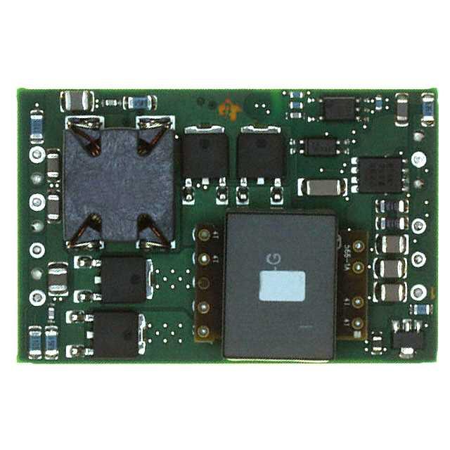
The PTB4851x uses double-sided surface mount
technology contruction. The package size is based on
the industry standard outline and does not require a
heatsink. Both through-hole and surface mount pin
configurations are available.
*VO2is the negative voltage.
UDG-07040
1
Please be aware that an important notice concerning availability, standard warranty, and use in critical applications of
Texas Instruments semiconductor products and disclaimers thereto appears at the end of this data sheet.
PRODUCTION DATA information is current as of publication date.
Products conform to specifications per the terms of the Texas
Instruments standard warranty. Production processing does not
necessarily include testing of all parameters.
Copyright © 2004–2007, Texas Instruments Incorporated
�Not Recommended for New Designs
PTB48510
PTB48511
SLTS219F – FEBRUARY 2004 – REVISED MARCH 2007
www.ti.com
ORDERING INFORMATION
BASE DEVICE NUMBER. (PTB4851xxx)
ORDER
PREFIX
PTB48510xxx
PTB48511xxx
(1)
(2)
(3)
(4)
OUTPUT VOLTAGE
(PTB4851xx)
DESCRIPTION
Basic model
Adds output overvoltage protection
(2)
PACKAGE OPTIONS (PT4851xx)
CODE
VOLTAGE
(V)
CODE
A
±5
AH
B
±12
C
±15 (4)
AS
PACKAGE
REFERENCE (1)
DESCRIPTION
Horizontal T/H
SMD, Standard
ERK
(3)
ERL
Reference the applicable package reference drawing for the dimensions and PC board layout
Output overvoltage protection
Standard option specifies 63/37, Sn/Pb pin solder material
±15-V output is not available with the PTB48511
Environmental and General Specifications
(Unless otherwise stated, all voltages are with respect to VI2)
VI
TA
VALUE
UNIT
Input Voltage Range
Over output load range
36 to 75
VDC
Isolation Voltage
Input-output/input/case
1500
V
Capacitance
Input to output
1500
pF
Resistance
Input to output
10
mΩ
Operating Temperature Range
Over VI Range
–40 to 85
OTP
Over-Temperature Protection
Treflow
Solder Reflow Temperature
Ts
Storage Temperature
Hysterisis
°C
235 (2)
–55 to 125
Mechanical Shock
Per Mil-STD-883D, Method 2002.3 T/H
1 ms, 1/2 Sine, mounted
SMD
Mechanical Vibration Mil-STD-883D
Mil-STD-883D, Method 2007.2
20-2000 Hz
Flammability
2
10
Surface temperature of module body or pins
Weight
(1)
(2)
115 (1)
Shutdown threshold
500
250
T/H
10
SMD
5
28
G
G
grams
Meets UL 94V-O
This parameter is assured by design.
During reflow of SMD package version do not elevate peak temperature of the module, pins or internal components above the stated
maximum.
Copyright © 2004–2007, Texas Instruments Incorporated
�Not Recommended for New Designs
PTB48510
PTB48511
www.ti.com
SLTS219F – FEBRUARY 2004 – REVISED MARCH 2007
ELECTRICAL CHARACTERISTICS
(Unless otherwise stated, TA = 25°C, VI = 48 V, CI = 0 μF, CO = 0 μF, IO1 = IO2 = 3.25 A maximum)
PARAMETER
PTB4851xA
TEST CONDITIONS
MIN
TYP
MAX
UNIT
PO
Output Power
Total output power from VO1 or VO2
0
65
(1)
W
IO1, IO2
Output Current
Over VI range, IO1 ≤ 0.1 A or IO2 ≤ 0.1 A
0
6.5 (2)
A
IO1 - IO2
Output Load Imbalance
IO1 ≤ 0.1 A or IO2 ≤ 0.1 A
0
1 (3)
A
VO1, VO2
Output Voltage
Includes set point, line, load, IO1 ≤ 0.1 A or IO2 ≤ 0.1 A
–40°C ≤ TA ≤ 85°C
4.75(2)
5 5.25(2)
V
ΔRegtemp
Temperature Variation
–40°C ≤ TA ≤ 85°C, IO1 ≤ 0.1 A or IO2 ≤ 0.1
A
VO1
±1
VO2
±1
ΔRegline
Line Regulation
Over VI range, balanced load
VO1 or VO2
±0.1
±0.4
%VO
ΔRegload
Load Regulation
Over IO1, IO2range, balanced load
VO1 or VO2
±0.2
±0.4
%VO
η
Efficiency
Vr
VO Ripple (pk-pk)
30 (4)
mVpp
ttr
Transient Response
ΔVtr
IOtrip
VO1(trip),
VO2(trip)
Overcurrent Threshold
86%
20 MHz bandwidth, CO = 10-μF tantalum capacitor
20
0.11 A/μs load step, 50% to 75% IO1 or IO2 maximum
30
VO1 or VO2 overshoot/undershoot
VI = 36 V, reset followed by auto-recovery
(5)
6.8
10
NA
NA
PTB48511
5.9
7
Short Circuit Current
Continuous overcurrent trip, IO1 = IO2
VO1(adj),
VO2(adj)
Output Voltage Adjust
Range
VO1 or VO2 adjust simultaneously
3.5
fS
Switching Frequency
Over VI and IO ranges
440
Undervoltage lockout
7.5
%VO
PTB48510
Outputs latched off
VI off
μs
±1.0
Overvoltage Threshold
VI on
%VO
IO1(pk) IO2(pk)
12.5
Duty
10%
470 (6)
VI increasing
33
VI decreasing
32
A
V
A
5.5
V
500
kHz
V
On/Off Enable (pin 3)
VIH
High-level input voltage
VIL
Low-level input voltage
IIL
Low-level input current
II standby
Standby Input Current
Pin 3 connected
tON
Start-up Time
IO1 ≤ 0.1 A or IO2 ≤ 0.1 A, VO1 or VO2 rising 0 to 0.95 (typ)
CI
Internal Input Capacitance
Referenced to VI (pin 4)
MTBF
Reliability
Per Telcordia SR-332 50% stress,
TA = 40°C, ground benign
(7)
(8)
0.8
6
10
0
PTB48510A
2.7
PTB48511A
2.5
V
mA
mA
22
ms
μF
3
Capacitance from either output to COM (pin 6)
(6)
–0.2
–1
External Output
Capacitance
(4)
(5)
75 (7)
2
CO
(1)
(2)
(3)
3.6
5000 (8
)
μF
106 hrs
See Safe Operating Area curves or contact the factory for the appropriate derating.
Under balanced load conditions, load current flowing out of VO1 is balanced to within ±0.1 A of that flowing into VO2.
A load imbalance is the difference in current flowing from VO1 to VO2. The module can operate with a higher imbalance but with reduced
specifications.
Output voltage ripple is measured with a 10-μF tantalum capacitor connected from VO1 (pin 5) or VO2 (pin 8), to COM (pin 6).
If the overvoltage threshold is exceeded by either regulated output the module will shut down, turning both outputs off. This is a latched
condition, which can only by reset by removing and then re-applying the module's input power.
This is the free-running frequency. The module can be made to synchronize with the PTB48500 when both modules are used together
in a system.
The On/Off Enable (pin 3) has an internal pull-up and may be controlled with an open-collector (or open-drain) transistor. The input is
diode protected and may be connected to VI. The open-circuit voltage is 5 V maximum. If it is left open circuit the converter operates
when input power is applied.
Electrolytic capacitors with very low equivalent series resistance (ESR) may induce instability when used on the output. Consult the
factory before using capacitors with organic, or polymer-aluminum type electrolytes.
Copyright © 2004–2007, Texas Instruments Incorporated
3
�Not Recommended for New Designs
PTB48510
PTB48511
SLTS219F – FEBRUARY 2004 – REVISED MARCH 2007
www.ti.com
ELECTRICAL CHARACTERISTICS
(Unless otherwise stated, TA = 25°C, VI = 48 V, CI = 0 μF, CO = 0 μF, IO1 = IO2 = 3.25 A maximum)
PARAMETER
PTB4851xB
TEST CONDITIONS
MAX
UNIT
PO
Output Power
Total output power from VO1or VO1
0
72 (1)
W
IO1 or IO2
Output Current
Over VI range, IO1 ≤ 0.1 A or IO2 ≤ 0.1 A ≤ 0.1 A
0
3 (2)
A
IO1 - IO2
Output Load Imbalance
IO1 ≥ 0.1 A, IO2 ≥ 0.1 A
0
1 (3)
A
VO1 or VO2
Output Voltage
Includes set point, line, load, IO1 ≤ 0.1 A or IO2 ≤ 0.1 A ≤
0.1 A
–40°C ≤ TA ≤ 85°C
11.6(2)
12 12.4(2)
V
ΔRegtemp
Temperature Variation
MIN
TYP
–40°C ≤ TA ≤ 85°C, IO1 ≤ 0.1 A or IO2 ≤ 0.1
A
VO1 or VO2
±1
%VO
ΔRegline
Line Regulation
Over VI range, balanced load
VO1 or VO2
±0.05
±0.5
%VO
ΔRegload
Load Regulation
Over IO1 or IO2 range, balanced load
VO1 or VO2
±0.1
±1
%VO
η
Efficiency
Vr
VO Ripple (pk-pk)
80 (4)
mVpp
ttr
Transient Response
ΔVtr
IOtrip
VO1(trip),
VO2(trip)
Overcurrent Threshold
89%
20 MHz bandwidth, CO = 10 μF tantalum capacitor
20
0.1 A/μs load step, 50% to 75% IO1 or IO2 maximum
30
VO1 or VO2 overshoot/undershoot
±1
VI = 36 V, reset followed by auto-recovery
(5)
3.3
PTB48510A
NA
PTB48511A
14
Overvoltage Threshold
Outputs latched off
Short Circuit Current
Continuous overcurrent trip, IO1 = IO2
VO1(adj),
VO2(adj)
Output Voltage Adjust
Range
VO1 and VO2 adjust simultaneously
6.5
fS
Switching Frequency
Over VI and IO ranges
440
VI on
VI off
Under-Voltage Lockout
On/Off Enable (pin 3)
μs
IO1(pk) IO2(pk)
3.8
%VO
5
NA
15.8
17
6
Duty
A
480 (6)
VI increasing
33
VI decreasing
32
13.4
V
500
kHz
V
Referenced to VI (pin 4)
High-level input voltage
3.6
75 (7)
VIL
Low-level input voltage
–0.2
0.8
IIL
Low-level input current
II standby
Standby Input Current
Pin 3 open circuit
tON
Start-up Time
IO1 ≤ 1 A or IO2 ≤ 1 A, VO1 or VO2 rising 0 to 0.95 (typ)
CI
Internal Input Capacitance
CO
External Output
Capacitance
Capacitance from either output to COM (pin 6)
MTBF
Reliability
Per Telcordia SR-332 50% stress,
TA = 40°C, ground benign
(4)
(5)
(6)
(7)
(8)
4
V
10%
VIH
(1)
(2)
(3)
A
–1
2
6
12
PTB48510B
2.8
PTB48511B
2.5
mA
mA
18
ms
μF
3
0
V
3000 (8
)
μF
106 Hrs
See Safe Operating Area curves or contact the factory for the appropriate derating.
Under balanced load conditions, load current flowing out of VO1 is balanced to within ±0.1 A of that flowing into VO2.
A load imbalance is the difference in current flowing from VO1 to VO2. The module can operate with a higher imbalance but with reduced
specifications.
Output voltage ripple is measured with a 10 μF tantalum capacitor connected from VO1 (pin 5) or VO2 (pin 8), to COM (pin 6).
If the overvoltage threshold is exceeded by either regulated output the module will shut down, turning both outputs off. This is a latched
condition, which can only by reset by removing and then re-applying the module's input power.
This is the free-running frequency. The module can be made to synchronize with the PTB48500 when both modules are used together
in a system.
The On/Off Enable (pin 3) has an internal pull-up and may be controlled with an open-collector (or open-drain) transistor. The input is
diode protected and may be connected to VI. The open-circuit voltage is 5 V maximum. If it is left open circuit the converter operates
when input power is applied.
Electrolytic capacitors with very low equivalent series resistance (ESR) may induce instability when used on the output. Consult the
factory before using capacitors with organic, or polymer-aluminum type electrolytes.
Copyright © 2004–2007, Texas Instruments Incorporated
�Not Recommended for New Designs
PTB48510
PTB48511
www.ti.com
SLTS219F – FEBRUARY 2004 – REVISED MARCH 2007
ELECTRICAL CHARACTERISTICS
(Unless otherwise stated, TA = 25°C, VI = 48 V, CI = 0 μF, CO = 0 μF, IO1 = IO2 = 3.25 A maximum)
PARAMETER
PTB4851xC
TEST CONDITIONS
MAX
UNIT
PO
Output Power
Total output power from VO1 or VO2
0
66 (1)
W
IO1 or IO2
Output Current
Over VI range, IO1 ≤ 0.1 A or IO2 ≤ 0.1 A
0
2.2 (2)
A
IO1 - IO2
Output Load Imbalance
IO1 ≤ 0.1 A or IO2 ≤ 0.1 A
0
1 (3)
A
VO1 or VO2
Output Voltage
Includes set point, line, load, IO1 - IO2 ≤ 0.1 A,
–40°C ≤ TA ≤ 85°C
14.5(2)
15 15.5(2)
V
ΔRegtemp
Temperature Variation
–40°C ≤ TA ≤ 85°C, IO1 ≤ 0.1 A or IO2 ≤ 0.1
A
VO1 or VO2
±1
ΔRegline
Line Regulation
Over VI range, balanced load
VO1 or VO2
±0.05
±0.5
%VO
ΔRegload
Load Regulation
Over IO1 or IO2 range, balanced load
VO1 or VO2
±0.1
±1
%VO
η
Efficiency
IO1 = IO2
Vr
VO Ripple (pk-pk)
20 MHz bandwidth, CO = 10 μF tantalum capacitor
50
100 (4)
mVpp
0.1 A/μs load step, 50% to 75% IO1 or IO2 maximum
30
μs
VO1 or VO2 overshoot/undershoot
±1
%VO
ttr
Transient Response
ΔVtr
IOtrip
VO1(adj) ,
VO2(adj)
fS
Over Current Threshold
Continuous overcurrent trip, IO1 = IO2
Output Voltage Adjust
Range
VO1 and VO2 adjust simultaneously
VI off
Under-Voltage Lockout
On/Off Enable (pin 3)
TYP
%VO
90%
VI = 36 V, reset followed by auto-recovery
Short Circuit Current
Switching Frequency
VI on
MIN
2.45
IO1(pk) IO2(pk)
Duty
Over VI and IO ranges
3
3.85
4.5
A
10%
7.2
440
480
(5)
VI increasing
33
VI decreasing
32
16.7
V
520
kHz
V
Referenced to –VI (pin 4)
VIH
High-level input voltage
3.6
75 (6)
VIL
Low-level input voltage
–0.2
0.8
IIL
Low-level input current
II standby
Standby Input Current
Pin 3 open circuit
tON
Start-up Time
IO1 ≤ 1 A or IO2 ≤ 1 A, VO1 or VO2 or rising 0 to 0.95 (typ)
CI
Internal Input Capacitance
CO
External Output
Capacitance
Capacitance from either output to COM (pin 6)
MTBF
Reliability
Per Telcordia SR-332 50% stress,
TA = 40°C, ground benign
(1)
(2)
(3)
(4)
(5)
(6)
(7)
A
–1
2
6
12
2.8
mA
mA
18
ms
μF
3
0
V
3000 (7
)
μF
106 hrs
See Safe Operating Area curves or contact the factory for the appropriate derating.
Under balanced load conditions, load current flowing out of VO1 is balanced to within ±0.1 A of that flowing into VO2.
A load imbalance is the difference in current flowing from VO1 to VO2. The module can operate with a higher imbalance but with reduced
specifications.
Output voltage ripple is measured with a 10-μF tantalum capacitor connected from VO1 (pin 5) or VO2 (pin 8), to COM (pin 6).
This is the free-running frequency. The module can be made to synchronize with the PTB48500 when both modules are used together
in a system.
The On/Off Enable (pin 3) has an internal pull-up and may be controlled with an open-collector (or open-drain) transistor. The input is
diode protected and may be connected to VI. The open-circuit voltage is 5 V maximum. If it is left open circuit the converter operates
when input power is applied.
Electrolytic capacitors with very low equivalent series resistance (ESR) may induce instability when used on the output. Consult the
factory before using capacitors with organic, or polymer-aluminum type electrolytes.
Copyright © 2004–2007, Texas Instruments Incorporated
5
�Not Recommended for New Designs
PTB48510
PTB48511
SLTS219F – FEBRUARY 2004 – REVISED MARCH 2007
www.ti.com
DEVICE INFORMATION
TERMINAL FUNCTIONS
TERMINAL
NAME
+VI
(1)
Sync In
Enable
DESCRIPTION
NO.
(2)
1
The positive input supply for the module with respect to VI (or ground return). When powering the module from
a –48 V telecom central office supply, this input is connected to the primary system ground.
2
This pin is used when the PTB4851x and PTB4850x DC/DC converter modules are used together. Connecting
this pin to the Sync Out of the PTB4850x module allows the PTB4851x to be synchronized to the same switch
conversion frequency as the PTB4850x.
3
This is an open-collector (open-drain) negative logic input that enables the module output. This pin is
referenced to –VI . A logic 0 at this pin enables the module's outputs, and a high impedance disables the
outputs. If this feature is not used the pin should be connected to –VI .
Note: Connecting this input directly to the EN Out pin of the PTB4850x enables the output voltages from both
converters (PTB4850x and PTB4851x) to power up in sequence.
-VI
4
The negative input supply for the module, and the 0 VDC reference for the Enable, and Sync In signals. When
the module is powered from a +48-V supply, this input is connected to the 48-V Return.
VO1
5
The positive output supply voltage, which is referenced to the COM node. The voltage at VO1 has the same
magnitude, but is the complement to that at VO2 .
VO2
8
The negative output supply voltage, which is referenced to the COM node. The voltage at VO2 has the same
magnitude, but is the complement to that at VO1 .
COM
6
The secondary return reference for the module's regulated output voltages. This node is dc isolated from the
input supply pins.
VOAdj
7
Using a single resistor, this pin allows the magnitude of both VO1 and VO2 to be adjusted together, either higher
or lower than their preset value. If not used, this pin should be left open circuit.
(1)
(2)
6
Shaded functions indicate signals that are referenced to -VI
Denotes negative logic: Open = Output Off, –VI = Normal operation.
Copyright © 2004–2007, Texas Instruments Incorporated
�Not Recommended for New Designs
PTB48510
PTB48511
www.ti.com
SLTS219F – FEBRUARY 2004 – REVISED MARCH 2007
TYPICAL CHARACTERISTICS
PTB4851xA CHARACTERISTIC DATA at VI = 48 V
(1) (2)
Characteristic data has been developed from actual products tested at 25°C. This data is considered typical data for the
converter.
EFFICIENCY
vs
LOAD CURRENT
POWER DISSIPATION
vs
LOAD CURRENT
100
CROSS REGULATION
12
300
10
200
PD - Power Dissipation - W
h - Efficiency - %
80
70
Cross Regulation - mV
D VO1 with IO1 = 1 A
90
8
6
4
60
0
1
5
2
3
4
(IO1 = IO2) - Load Current - A
Figure 1.
6
-100
-300
0
0
1
2
3
4
5
(IO1 = IO2) - Load Current - A
(1)
Figure 2.
0
6
1
2
3
4
IO2 - Load Current - A
5
6
Figure 3.
(1)
CROSS REGULATION
SAFE OPERATING AREA
90
300
D VO2 with IO2 = 1 A
80
TA - Ambient Temperature - °C
200
Cross Regulation - mV
0
-200
2
50
100
100
0
-100
-200
70
400 LFM
200 LFM
60
50
100 LFM
40
Natural
Convection
30
VI = 48 VDC
-300
0
1
2
3
4
IO1 - Load Current - A
Figure 4.
(1)
(2)
5
6
20
0
1
2
3
4
5
(IO1 = IO2) - Load Current - A
Figure 5.
6
(1) (2)
Under a balanced load, current flowing out of VO1 is equal to that flowing into VO2.
SOA curves represent the conditions at which internal components are at or below the manufacturer's maximum operating
temperatures. Derating limits apply to modules soldered directly to a 4 in. × 4 in. double-sided PCB with 1 oz. copper.
Copyright © 2004–2007, Texas Instruments Incorporated
7
�Not Recommended for New Designs
PTB48510
PTB48511
SLTS219F – FEBRUARY 2004 – REVISED MARCH 2007
www.ti.com
TYPICAL CHARACTERISTICS (Continued)
PTB4851xB CHARACTERISTIC DATA at VI = 48 V
(1) (2)
Characteristic data has been developed from actual products tested at 25°C. This data is considered typical data for the
converter.
EFFICIENCY
vs
LOAD CURRENT
POWER DISSIPATION
vs
LOAD CURRENT
CROSS REGULATION
400
12
100
D VO1 with IO1 = 1 A
10
80
70
200
Cross Regulation - mV
PD - Power Dissipation - W
h - Efficiency - %
90
8
6
4
0
-200
60
2
50
0
0.5
2.0
1.0
1.5
(IO1 = IO2) - Load Current - A
Figure 6.
2.5
3.0
-400
0
0
0.5
(1)
1.0
1.5
2.0
(IO1 = IO2) - Load Current - A
Figure 7.
2.5
0.5
1.0
1.5
2.0
IO2 - Load Current - A
2.5
3.0
Figure 8.
(1)
CROSS REGULATION
SAFE OPERATING AREA
90
400
D VO2 with IO2 = 1 A
TA - Ambient Temperature - °C
80
200
Cross Regulation - mV
0
3.0
0
-200
70
400 LFM
200 LFM
60
50
100 LFM
40
Natural
Convection
30
VI = 48 VDC
-400
0
0.5
1.0
1.5
2.0
IO1 - Load Current - A
Figure 9.
(1)
(2)
8
2.5
3.0
20
0
0.5
1.0
1.5
2.0
(IO1 = IO2) - Load Current - A
Figure 10.
2.5
3.0
(1) (2)
Under a balanced load, current flowing out of VO1 is equal to that flowing into VO2.
SOA curves represent the conditions at which internal components are at or below the manufacturer's maximum operating
temperatures. Derating limits apply to modules soldered directly to a 4 in. × 4 in. double-sided PCB with 1 oz. copper.
Copyright © 2004–2007, Texas Instruments Incorporated
�Not Recommended for New Designs
PTB48510
PTB48511
www.ti.com
SLTS219F – FEBRUARY 2004 – REVISED MARCH 2007
TYPICAL CHARACTERISTICS (Continued)
PTB4851xC CHARACTERISTIC DATA at VI = 48 V
(1) (2)
Characteristic data has been developed from actual products tested at 25°C. This data is considered typical data for the
converter.
EFFICIENCY
vs
LOAD CURRENT
POWER DISSIPATION
vs
LOAD CURRENT
100
10
90
8
CROSS REGULATION
300
80
70
Cross Regulation - mV
PD - Power Dissipation - W
h - Efficiency - %
D VO1 with IO1 = 1 A
200
6
4
2
60
0
0.3
1.5
1.2
1.8
0.6
0.9
(IO1 = IO2) - Load Current - A
Figure 11.
2.1
-100
-300
0
0.3
0.6
0.9
1.2
1.5
1.8
(IO1 = IO2) - Load Current - A
(1)
Figure 12.
2.1
0
0.3
0.6
0.9
1.2
1.5
IO2 - Load Current - A
1.8
2.1
Figure 13.
(1)
CROSS REGULATION
SAFE OPERATING AREA
90
300
D VO2 with IO2 = 1 A
80
TA - Ambient Temperature - °C
200
Cross Regulation - mV
0
-200
0
50
100
100
0
-100
-200
70
400 LFM
200 LFM
60
100 LFM
50
Natural
Convection
40
30
VI = 48 VDC
-300
0
0.3
0.6
0.9
1.2
1.5
IO1 - Load Current - A
Figure 14.
(1)
(2)
1.8
2.1
20
0
0.5
1.0
1.5
2.0
(IO1 = IO2) - Load Current - A
Figure 15.
2.5
3.0
(1) (2)
Under a balanced load, current flowing out of VO1 is equal to that flowing into VO2.
SOA curves represent the conditions at which internal components are at or below the manufacturer's maximum operating
temperatures. Derating limits apply to modules soldered directly to a 4 in. × 4 in. double-sided PCB with 1 oz. copper.
Copyright © 2004–2007, Texas Instruments Incorporated
9
�Not Recommended for New Designs
PTB48510
PTB48511
SLTS219F – FEBRUARY 2004 – REVISED MARCH 2007
www.ti.com
APPLICATION INFORMATION
ADJUSTING THE OUTPUT VOLTAGE OF THE PTB4851x SERIES OF DC/DC CONVERTERS
The PTB48510 and PTB48511 DC/DC converters produce a balanced pair of complimentary output voltages.
They are identified VO1 and VO2, respectively. The magnitude of both output voltages can be adjusted together as
a pair, higher or lower, by up to ±10% of their nominal. The adjustment method uses a single external resistor.1
The value of the resistor determines the adjustment magnitude, and its placement determines whether the
magnitude is increased or decreased. The resistor values can be calculated using the appropriate formula (see
below). The formula constants are given in Table 1. The placement of each resistor is as follows.
Adjust Up: To increase the magnitude of both output voltages, place a resistor R1 between VO 1Adj (pin 7) and
the VO2 (pin 8) voltage rail; see Figure 16.
Adjust Down: To decrease the magnitude of both output voltages, add a resistor (R2), between VOAdj (pin 7)
and the VO1 (pin 5) voltage rail; see Figure 17.
PTB48510
PTB48510
VO1
5
COM
6
VOAdj
7
VO1
5
VO1
R2
Adjust Down
R1
Adjust Up
VO2
VO1
8
VO2
UDG-07041
Figure 16. Adjust Up Resistor Placement
VOAdj
7
COM
6
VO2
8
VO2
UDG-07042
Figure 17. Adjust Down Resistor Placement
ADJUST RESISTOR CALCULATION
The value of the adjust resistor is calculated using one of the following equations. Use the equation for R1 to
adjust up, or (R2) to adjust down.
V r Ro
R [Adjust Up] +
* Rs kW
1
2ǒVa * VoǓ
(1)
ǒ
Ǔ
* R s kW
2 ǒV o * VaǓ
ǒR2Ǔ [Adjust Down] + Ro 2 V a * V r
(2)
Where:
VO = Magitude of the original VO1 or VO2
Va = Magnitude of the adjusted voltage
Vr = The reference voltage from Table 1
RO = The resistance value in Table 1
RS = The series resistance from Table 1
10
Copyright © 2004–2007, Texas Instruments Incorporated
�Not Recommended for New Designs
PTB48510
PTB48511
www.ti.com
SLTS219F – FEBRUARY 2004 – REVISED MARCH 2007
Table 1. Adjustment Range and Formula Parameters
PARAMETERS
PTB4851xA
PTB4851xB
PTB48510C
VO(nom) (V)
5
12
15
Va(min) (V)
3.5
6.5
7.2
Va(max) (V)
5.5
13.4
16.7
2.495
2.495
2.495
Rn (kΩ)
Vr
7.5
18.2
22.1
Rs (kΩ)
9.09
16.9
16.9
(V)
NOTES:
1. A 0.05 W rated resistor may be used. The tolerance should be 1%, with a temperature stability of 100
ppm/°C or better. Place the resistor in either the R1 or (R2) location, as close to the converter as possible.
2. Never connect capacitors to the Vo Adj pin. Capacitance added to this pin can affect the stability of the
regulated output.
3. The overvoltage protection (PTB48511x) is nominally set to 25% above the original output voltage setpoint. Increasing the magnitude of the output voltages reduces the margin between the output voltage and
the overvoltage (OV) protection threshold. This could make the module more sensitive to OV faults, as a
result of random noise and load transients.
Note: An OV fault is a latched condition that shuts down the converter's outputs. The fault can be cleared by
cycling the Enable pin, or by momentarily removing input power to the module.
CONFIGURING THE PTB4850x and PTB4851x DC/DC CONVERTERS FOR DSL APPLICATIONS
When operated as a pair, the PTB4850x and PTB4851x converters are specifically designed to provide all the
required supply voltages for powering xDSL chipsets. The PTB4850x produces two logic voltages. They include
a 3.3-V source for logic and I/O, and a low-voltage for powering a digital signal processor core. The PTB4851x
produces a balanced pair of complementary supply voltages that is required for the xDSL transceiver ICs. When
used together in these types of applications, the PTB4850x and PTB4851x may be configured for power-up
sequencing, and also synchronized to a common switch conversion frequency. Figure 19 shows the required
cross-connects between the two converters to enable these two features.
SWITCHING FREQUENCY SYNCHRONIZATION
Unsynchronized, the difference in switch frequency introduces a beat frequency into the input and output AC
ripple components from the converters. The beat frequency can vary considerably with any slight variation in
either converter’s switch frequency. This results in a variable and undefined frequency spectrum for the ripple
waveforms, which would normally require separate filters at the input of each converter. When the switch
frequency of the converters are synchronized, the ripple components are constrained to the fundamental and
higher. This simplifies the design of the output filters, and allows a common filter to be specified for the treatment
of input ripple.
POWER-UP SEQUENCING
The desired power-up sequence for the AC7 supply voltages requires that the two logic-level voltages from the
PTB4850x converter rise to regulation prior to the two complementary voltages that power the transceiver ICs.
This sequence cannot be assured if the PTB4850x and PTB4851x are allowed to power up independently,
especially if the 48-V input voltage rises relatively slowly. To ensure the desired power-up sequence, the EN Out
pin of the PTB4850x is directly connected to the activelow Enable input of the PTB4851x (see Figure 19). This
allows the PTB4850x to momentarily hold off the outputs from the PTB4851x until the logic-level voltages have
risen first. Figure 19 shows the power-up waveforms of all four supply voltages from the schematic of Figure 19.
Copyright © 2004–2007, Texas Instruments Incorporated
11
�Not Recommended for New Designs
PTB48510
PTB48511
SLTS219F – FEBRUARY 2004 – REVISED MARCH 2007
www.ti.com
VCCIO
(1 V/div)
VCORE
(1 V/div)
+VTCVR
(5 V/div)
+VTCVR
(5 V/div)
T - Time - 10 ms/div
Figure 18. Power-Up Sequencing Waveforms
9
VOAdj
PTB48500A
-48 VRTN
+
Input
Filter
-48 V
1
+VI
VO1 10
3
Enable
VO2
6
VCORE
POR
8
POR
5
-VI
COM
7
VCCIO
EN Out Sync Out
4
2
2
7
Sync In
VOAdj
PTB48510A
1
+VI
VO1
5
3
Enable
COM
6
4
-VI
VO2
8
+VTCVR
-VTCVR
UDG-07043
Figure 19. Example of PTB4850x and PTB4851x Modules Configured for DSL Applications
12
Copyright © 2004–2007, Texas Instruments Incorporated
�PACKAGE OPTION ADDENDUM
www.ti.com
19-Dec-2019
PACKAGING INFORMATION
Orderable Device
Status
(1)
Package Type Package Pins Package
Drawing
Qty
Eco Plan
Lead/Ball Finish
MSL Peak Temp
(2)
(6)
(3)
Op Temp (°C)
Device Marking
(4/5)
PTB48510BAS
NRND
Surface
Mount Module
ERL
8
9
Non-RoHS
& non-Green
SNPB
Level-1-235C-UNLIM/
Level-3-260C-168HRS
-40 to 85
PTB48510CAH
NRND
ThroughHole Module
ERK
8
9
RoHS (In Work)
& non-Green
SN
N / A for Pkg Type
-40 to 85
(1)
The marketing status values are defined as follows:
ACTIVE: Product device recommended for new designs.
LIFEBUY: TI has announced that the device will be discontinued, and a lifetime-buy period is in effect.
NRND: Not recommended for new designs. Device is in production to support existing customers, but TI does not recommend using this part in a new design.
PREVIEW: Device has been announced but is not in production. Samples may or may not be available.
OBSOLETE: TI has discontinued the production of the device.
(2)
RoHS: TI defines "RoHS" to mean semiconductor products that are compliant with the current EU RoHS requirements for all 10 RoHS substances, including the requirement that RoHS substance
do not exceed 0.1% by weight in homogeneous materials. Where designed to be soldered at high temperatures, "RoHS" products are suitable for use in specified lead-free processes. TI may
reference these types of products as "Pb-Free".
RoHS Exempt: TI defines "RoHS Exempt" to mean products that contain lead but are compliant with EU RoHS pursuant to a specific EU RoHS exemption.
Green: TI defines "Green" to mean the content of Chlorine (Cl) and Bromine (Br) based flame retardants meet JS709B low halogen requirements of