Not Recommended for New Designs
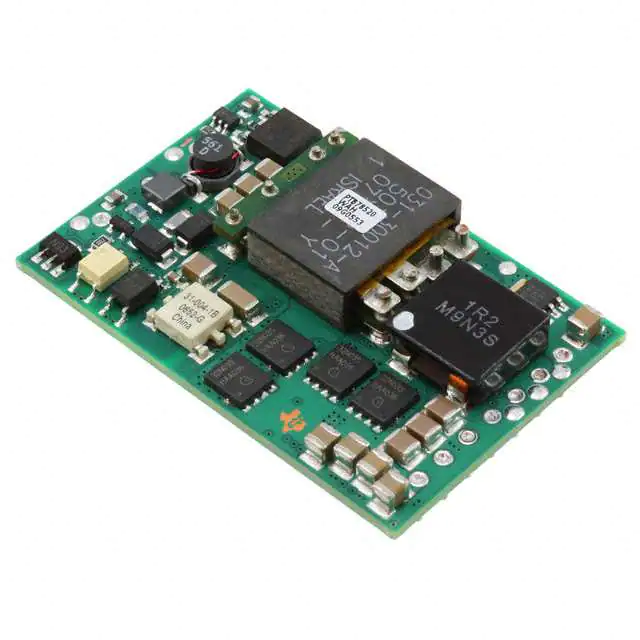
PTB78520W
20-A, 18–60-V Input Auto-Track
Compatible Isolated DC/DC Converter
SLTS226A – JULY 2004 – REVISED OCTOBER 2005
Features
• Wide-Input Voltage Range:
18 V to 60 V
• 20 A Total Output Current
• 90% Efficiency
• Wide-Adjust Output Voltage:
1.8 V to 3.6 V
• Over-Current Protection
• Output Over-Voltage Protection
• Over-Temperature Shutdown
• Output Enable Control
• Auto-Track Compatible
Sequenced Output
• Smart-Sense Remote Sensing
• Under-voltage Lockout
• Industry Standard Footprint
• Surface Mountable
• 1500 VDC Isolation
• Agency Approvals (Pending):
UL/cUL 60950, EN 60950
Description
Pin-Out Information
nation of input-output isolation and a
wide-input voltage range, allows operation
from either +24 V or –48 V. The wideoutput adjust enables the output voltage
to be set to to any voltage over the range,
1.8 V to 3.6 V, using a single external
resistor. Precise output voltage regulation is assured using Smart-Sense. This
is a differential remote sense that will
intelligently regulate the sequenced output, depending on its sequence status.
Other operational features include an
input under-voltage lockout (UVLO) and
an output enable control. Over-current,
over-voltage, and over-temperature protection assures the module’s ability to
survive any load fault.
Typical applications include distributed
power architectures in both telecom and
computing environments, particularly
complex digital systems requiring powersequencing of multiple power supply rails.
The PTB78520W is a 20-A rated,
wide-input (18-60 V) isolated DC/DC
converter that incorporates Auto-Track™
power-up sequencing. This allows these
modules to simultaneously power up with
any other downstream non-isolated, AutoTrack compliant module.
The PTB78520W module provides
two outputs, each regulated to the same
voltage. During power up, the voltage at
‘VO Bus’ rises first, allowing this output
to provide input power to any downstream
non-isolated module. The voltage from
‘VO Seq’ is then allowed to rise simultaneously, under the control of Auto-Track,
along with the outputs from the downstream modules.
Whether used to facilitate power-up
sequencing, or operated as a stand-alone
module, the PTB78520W includes many
features expected of high-performance
DC/DC converter modules. The combi-
Pin Function
1
2
3
4
5
6
7
8
9
10
+VIN
VO Enable *
–VIN
Track
VO Com
(–) Sense
Vo Adjust
(+) Sense
VO Bus
VO Seq
Shaded functions indicate signals
electrically common with the input.
* Denotes negative logic:
Low (–VIN ) = Normal operation
Open = Output off
rack™
Auto-T cing
n
Seque
Typical Application
Simultaneous Powerup
V1
Track
4
V2
PTB78520W
+Sense
+VI
1
VO Seq
+VI
VO Bus
2
VO Enable
VO Adjust
8
V1 =3.3 V
10
9
2
Track
7
3
VO COM
–VI
3
–VI
–Sense
For technical support and further information visit http://power.ti.com
5
6
RSET
887
C1
100 µF
VI
PTH03050W VO
V2 =1.8 V
6
Inhibit GND Adjust
4
1
5
R1
5.49 k
C2
100 µF
�Not Recommended for New Designs
PTB78520W
20-A, 18–60-V Input Auto-Track
Compatible Isolated DC/DC Converter
SLTS226A – JULY 2004 – REVISED OCTOBER 2005
Ordering Information
Output Voltage (PTB78520❒xx)
Package Options (PTB78520x❒❒)
Code
W
Code
AH
AS
Voltage
1.8 V to 3.6 V
Description
Horiz. T/H
SMD, Standard (2)
Pkg Ref.
(ERP)
(ERQ)
(1)
Notes: (1) Reference the applicable package reference drawing for the dimensions and PC board layout
(2) “Standard” option specifies 63/37, Sn/Pb pin solder material.
Pin Descriptions
+VIN: The positive input for the module with respect to
–VIN. When powering the module from a negative input
voltage, this input is connected to the input source ground.
–VIN: The negative input supply for the module, and the
0-V reference for the ‘VO Enable’ input. When powering
the module from a positive source, this input is connected
to the input source return.
Vo Enable*: An open-collector (open-drain) negative logic
input that is referenced to –VIN. This input must be pulled
to –Vin potential to enable the output voltage. A highimpedance connection will disable the module output. If
the output enable feature is not used, pin 2 should be
permanently connected to –VIN. The module will then
produce an output whenever a valid input source is applied.
Vo Bus: Produces a positive power output with respect
to ‘VO COM’. This is the main output from the converter
when operated in a stand-alone configuration. It is dcisolated from the input power pins and is the first output
to rise when the converter is either powered or enabled.
In power-up sequencing applications, this output can
provide a 3.3-V standby source to power the downstream
non-isolated modules.
Vo Seq: This is the sequenced output voltage from the
converter. This voltage can be directly controlled from
the Track pin. During power up, VO Seq will rise with
the Track pin voltage, typically 20 ms after the VO Bus
output has reached regulation.
Vo COM: This is the output power return for both the
‘VO Bus’ and ‘VO Seq’ output voltages. This node should
be connected to the load circuit common.
Track: The voltage at this pin directly controls the voltage
at the ‘VO Seq’ regulated output. It is primarily used
to sequence the voltage at ‘VO Seq’ with the regulated
outputs from any downstream non-isolated modules that
are powered from the converter’s ‘+VO Bus’ output. In
these applications, the ‘Track’ pin is simply connected
to the track control of each of the non-isolated modules. The ‘Track’ pin of the PTB78520W has an internal
transistor, which holds it at ‘VO COM’ potential for
approximately 20 ms after the ‘VO Bus’ output is in
regulation. Following this delay, the ‘Track’ voltage and
‘VO Seq’ will rise simultaneously with the output voltage
from all the non-isolated modules, that are under the control of Auto-Track.
Vo Adjust: A resistor must be connected between this pin
and ‘–Sense’ to set the converter’s output voltage. A
0.05-W rated resistor may be used, with tolerance and
temperature stability of 1% and 100 ppm/°C, respectively.
If this pin is left open, the converter output voltage will
default to its lowest value. The specification table gives
the preferred resistor values for the popular bus voltages.
+Sense: The ‘+Sense’ pin can be connected to either the
‘VO Bus’ or ‘VO Seq’ outputs. When connected to ‘VO Seq’,
remote sense compensation will be delayed until the
power-up sequence is complete. The voltage at ‘Vo Bus’
will also be raised slightly. The pin may be left open
circuit, but connecting it to one of the output terminals
improves load regulation of that output.
–Sense: Provides the converter with a remote sense capability when used in conjunction with +Sense. For optimum
output voltage accuracy this pin should always be connected
to ‘VO COM’. This pin is also the reference connection for the output voltage set-point resistor.
For technical support and further information visit http://power.ti.com
�Not Recommended for New Designs
PTB78520W
20-A, 18–60-V Input Auto-Track
Compatible Isolated DC/DC Converter
SLTS226A – JULY 2004 – REVISED OCTOBER 2005
Environmental & Absolute Maximum Ratings
Characteristics
Symbols
Conditions
Min
Typ
Input Voltage
Track Input Voltage
Track Input Current
Operating Temperature Range
Over-Temperature Protection
Solder Reflow Temperature
Storage Temperature
Mechanical Shock
VIN
VTRACK
ITRACK (max)
TA
OTP
TREFLOW
TS
Surge (100 ms maximum)
—
0
—
–40
—
—
–40
—
—
—
—
—
—
—
—
—
115
—
—
250
150
15
5
28.5
Mechanical Vibration
Weight
Flammability
—
—
From external source
Over VIN Range
PCB temperature (near pin 1)
Surface temperature of module or pins
—
Per Mil-STD-883D, Method 2002.3
1 msec, ½ Sine, mounted
Mil-STD-883D, Method 2007.2
20-2000 Hz, PCB mounted
T/H
SMD
T/H
SMD
Max
75
VO Bus + 0.3
10 (i)
+85
—
235 (ii)
+125
—
—
—
—
—
Units
V
V
mA
°C
°C
°C
°C
Gs
Gs
grams
Meets UL 94V-O
Notes: (i) When the Track input is fed from an external voltage source, the input current must be limited. A 2.74-k Ω value series resistor is recommended.
(ii) During solder reflow of SMD package version, do not elevate the module PCB, pins, or internal component temperatures above a peak of 235 °C.
Specifications
(Unless otherwise stated, T A =25 °C, VIN =24 V, V O =3.3 V, CO =0 µF, and IO =IOmax)
PTB78520W
Characteristic
Symbol
Conditions
Min
Typ
Max
Units
Output Current
Over VIN range
0
0
0
18
—
—
—
—
—
—
—
—
48
±0.6 (3)
±0.8
±1
±1
±1.5
20 (1)
10 (1) (2)
20
60
—
—
—
—
±3 (3)
A
Input Voltage Range
Set Point Voltage Tolerance
Temperature Variation
Line Regulation
Load Regulation
Total Output Voltage Variation
IO bus
IO seq
IO tot
VIN
VO tol
Regtemp
Regline
Regload
∆VOtot
Output Voltage Adjust Range
Efficiency
∆VADJ
η
Vo Ripple (pk-pk)
Transient Response
VR
tTR
∆VTR
1.8
—
—
—
—
—
—
—
—
90
88.5
87
86.5
20
75
±3
3.6
—
—
—
—
—
—
—
mVpp
µs
%VO
—
0
0.1 (4)
—
—
—
–0.13
VO Bus
1
mA
V
V/ms
2
–0.2
—
—
—
—
—
15.5
225
—
0
1,500
—
10
1.2
—
—
–240
2
85
30
125
17
275
3
open (5)
+0.8
—
—
—
—
—
18
325
—
5,000
—
—
—
—
V
Track Input (pin 4)
Input Current
Open Circuit Voltage
Track Slew Rate Capability
Output Enable Input (pin 2)
Input High Voltage
Input Low Voltage
Input Low Current
Standby Input Current
No-Load Input Current
Over-Current Threshold
Output Over-Voltage Protection
Under-Voltage Lockout
Switching Frequency
Internal Input Capacitance
External Output Capacitance
Isolation Voltage
Capacitance
Resistance
Reliability
ITRACK
VTRACK
dVTRACK/dt
VIH
VIL
IIL
IIN standby
IIN no-load
ITRIP
OVP
UVLO
ƒS
CIN
COUT
MTBF
Sum total IO bus + IO seq
Over IO Range
–40° ≤TA ≤ +85°C
Over VIN range
Over IO range
Includes set-point, line, load,
–40° ≤TA ≤ +85°C
Over Vin range
IO =10 A
RSET =887 Ω,
RSET =6.98 kΩ,
RSET =35.7 kΩ,
RSET =open cct.
20 MHz bandwidth
1 A/µs load step, 50% to 100% IOmax
VO over/undershoot
pin connected to VO COM
Referenced to –VIN (pin 3)
pin 2 open
pins 2 & 3 connected, Io TOT =0
Shutdown, followed by auto-recovery
Output shutdown and latch off
Over VIN range
Between +Vo and –Vo
Input-output & input-case
Input-output
Input-output
Telcordia TR-332
50% stress, TA =40°C, ground benign
VO =3.3 V
VO =2.5 V
VO =2.0 V
VO =1.8 V
—
1,000
—
—
A
V
%VO
%VO
mV
mV
%VO
V
%
µA
mA
mA
A
%VO
V
kHz
µF
µF
Vdc
pF
MΩ
106 Hrs
Notes: (1) See SOA curves or consult factory for appropriate derating.
(2) When load current is supplied from the VO SEQ output, the module will exhibit higher power dissipation and slightly lower operating efficiency.
(3) The set-point voltage tolerance is affected by the tolerance and stability of R SET. The stated limit is unconditionally met if RSET has a tolerance of 1%,
with 100 ppm/°C temperature stability.
(4) When controlling the Track input from an external source the slew rate of the applied signal must be greater than the minimum limit. Failure to allow
the voltage to completely rise to the voltage at the Vo Bus output, at no less than the minimum specified rate, may thermally overstress the converter.
(5) The ‘VO Enable’ input has an internal pull-up, and if left open the converter output will be turned off. A discrete MOSFET or bipolar transistor is
recommended to control this input. The open-circuit voltage is approximately 20% of the input voltage. If the output enable feature is not used, this pin
should be permanently connected to –VIN . See application notes for other interface considerations.
For technical support and further information visit http://power.ti.com
�Not Recommended for New Designs
Typical Characteristics
PTB78520W
20-A, 18–60-V Input Auto-Track
Compatible Isolated DC/DC Converter
SLTS226A – JULY 2004 – REVISED OCTOBER 2005
Characteristic Data; VIN =24 V (See Note A)
Characteristic Data; VIN =48 V (See Note A)
Efficiency vs. Load Current (IO Bus)
Efficiency vs. Load Current (IO Bus)
100
100
90
90
3.3V
2.5V
2.0V
1.8V
80
70
VOUT
Efficiency - (%)
Efficiency - (%)
VOUT
60
3.3V
2.5V
2.0V
1.8V
80
70
60
50
50
0
4
8
12
16
20
0
4
8
Io Bus - (A)
12
16
20
Io Bus - (A)
Output Ripple vs. Load Current (I O Bus)
Output Ripple vs. Load Current (I O Bus)
50
50
40
40
3.3V
2.5V
2.0V
1.8V
30
20
VOUT
Ripple - (mV)
Ripple - (mV)
VOUT
10
3.3V
2.5V
2.0V
1.8V
30
20
10
0
0
0
4
8
12
16
20
0
4
8
Io Bus - (A)
16
20
Power Dissipation vs. Load Current (I O Bus)
Power Dissipation vs. Load Current (I O Bus)
12
12
10
VOUT
8
3.3V
2.5V
2.0V
1.8V
6
4
2
Power Dissipation - (W)
10
Power Dissipation - (W)
12
Io Bus - (A)
VOUT
8
3.3V
2.5V
2.0V
1.8V
6
4
2
0
0
0
4
8
12
Io Bus - (A)
16
20
0
5
10
15
20
Io Bus - (A)
Note A: All data listed in the above graphs has been developed from actual products tested at 25 °C. This data is considered typical data for the DC-DC Converter.
For technical support and further information visit http://power.ti.com
�Not Recommended for New Designs
Typical Characteristics
PTB78520W
20-A, 18–60-V Input Auto-Track
Compatible Isolated DC/DC Converter
SLTS226A – JULY 2004 – REVISED OCTOBER 2005
Safe Operating Areas; VIN =24 V (See Note B)
Safe Operating Areas; VIN =48 V (See Note B)
Load Current from ‘+V O Bus’ Output
Load Current from ‘VO Bus’ Output
90
90
80
Airflow
70
400LFM
200LFM
100LFM
Nat conv
60
50
40
Ambient Temperature (°C)
Ambient Temperature (°C)
80
30
Airflow
70
400LFM
200LFM
100LFM
Nat conv
60
50
40
30
20
20
0
4
8
12
16
20
0
4
Output Current (A)
12
16
20
Load Current from ‘VO Seq’ Output
Load Current from ‘+VO Seq’ Output
90
90
80
80
70
Airflow
60
100LFM
Nat conv
50
40
30
Ambient Temperature (°C)
Ambient Temperature (°C)
8
Output Current (A)
70
Airflow
60
200LFM
100LFM
Nat conv
50
40
30
20
20
0
2
4
6
8
10
Output Current (A)
0
2
4
6
8
10
Output Current (A)
Note B: SOA curves represent operating conditions at which internal components are at or below manufacturer’s maximum rated operating temperature.
For technical support and further information visit http://power.ti.com
�Not Recommended for New Designs
Application Notes
PTB78520W
Operating Features and System Considerations
for the PTB78520W DC/DC Converter
Over-Current Protection
To protect against load faults these converters incorporate
output over-current protection. Applying a load to the
output that exceeds the converter’s over-current threshold
(see applicable specification) will cause the output voltage
to momentarily fold back, and then shut down. Following
shutdown the module will periodically attempt to automatically recover by initiating a soft-start power-up.
This is often described as a “hiccup” mode of operation,
whereby the module continues in the cycle of successive
shutdown and power up until the load fault is removed.
Once the fault is removed, the converter automatically
recovers and returns to normal operation.
Output Over-Voltage Protection
The converter continually monitors for an output overvoltage (OV) condition, directly across the ‘+VO Bus’
output. The OV threshold automatically tracks the output voltage setpoint to a level that is 25% higher than
that set by the external RSET voltage adjust resistor. If
the output voltage exceeds this threshold, the converter
is immediately shut down and remains in a latched-off
state. To resume normal operation the converter must be
actively reset. This can only be done by momentarily
removing the input power to the converter. For failsafe
operation and redundancy, the OV protection uses circuitry that is independent of the converter’s internal
feedback loop.
Leaving the (+)Sense and (–)Sense pins open will not
damage the converter or load circuitry. The converter
includes default circuitry that keeps the output voltage in
regulation. If the remote sense feature is not used, the
(–)Sense pin should always be connected to ‘Vo COM’.
Note: The remote sense feature is not designed to compensate
for the forward drop of non-linear or frequency dependent
components that may be placed in series with the converter
output. Examples include OR-ing diodes, filter inductors,
ferrite beads, and fuses. When these components are enclosed
by the sense pin connections they are effectively placed inside
the regulation control loop, which can adversely affect the
stability of the converter.
Over-Temperature Protection
Over-temperature protection is provided by an internal
temperature sensor, which monitors the temperature of
the converter’s PCB (close to pin 1). If the PCB temperature exceeds a nominal 115 °C, the converter will
shut down. The converter will then automatically restart
when the sensed temperature drops back to approximately
105 °C. When operated outside its recommended thermal derating envelope (see data sheet SOA curves), the
converter will typcially cycle on and off at intervals from
a few seconds to one or two minutes. This is to ensure
that the internal components are not permanently damaged from excessive thermal stress.
Differential Output Voltage Sense
A differential remote sense allows a converter’s regulation circuitry to compensate for limited amounts of IR
drop, that may be incurred between the converter and
load, in either the positive or return PCB traces. Connecting the (+)Sense and (–)Sense pins to the respective
positive and ground reference of the load terminals will
improve the load regulation of the converter’s output
voltage at that connection point. The (–)Sense pin should
always be connected to the ‘VO COM’. The (+)Sense pin
may be connected to either the ‘+VO Bus’ or ‘+VO Seq’
outputs.
Under-Voltage Lockout
The Under-Voltage Lock-Out (UVLO) is designed to
prevent the operation of the converter until the input
voltage is close to the minimum operating voltage. The
converter is held off when the input voltage is below the
UVLO threshold, and turns on when the input voltage
rises above the threshold. This prevents high start-up
current during normal power-up of the converter, and
minimizes the current drain from the input source during low input voltage conditions. The converter will
meet full specifications when the minimum specified
input voltage is reached. The UVLO circuitry also overrides the operation of the Vo Enable control. Only when
the input voltage is above the UVLO threshold will the
Vo Enable control be functional.
When the (+)Sense pin is connected to the ‘VO Seq’
output, the voltage at ‘Vo Bus’ voltage will regulate
slightly higher. Depending on the load conditions on the
‘VO Seq’ output, the voltage at ‘VO Bus’ may be up to
100 mV higher than the converter’s set-point voltage.
In addition, the Smart-Sense feature (incorporated into
the PTB78520 converter) will only engage sense compensation to the ‘VO Seq’ output when that output voltage is
close to the set-point. During other conditions, such as
power-up and power-down sequencing events, the sense
circuit automatically defaults to sensing the ‘VO Bus’
voltage, internal to the converter.
Primary-Secondary Isolation
These converters incorporate electrical isolation between
the input terminals (primary) and the output terminals
(secondary). All converters are tested to a withstand voltage of 1500 VDC. This complies with UL/cUL 60950
and EN 60950 and the requirements for operational isolation. It allows the converter to be configured for either a
positive or negative input voltage source. The data sheet
‘Pin Descriptions’ section provides guidance as to the
correct reference that must be used for the external control signals.
For technical support and further information visit http://power.ti.com
�Not Recommended for New Designs
Application Notes
PTB78520W
Output Voltage Adjustment
The ‘VO Adjust’ control sets the output voltages to a value
higher than 1.8 V. For output voltages other than 1.8 V a
single external resistor, RSET, must be connected directly
between the ‘VO Adjust’ (pin 7) and ‘(–)Sense’ (pin 6) pins.
A 0.05-W rated resistor can be used. The tolerance should
be 1%, with a temperature stability of 100 ppm/°C (or
better). Place the resistor close to the converter and
connect it directly between pins 7 & 6 using dedicated
PCB traces (see typical application). Table 1-1 gives the
preferred value of the external resistor for a number of
standard voltages, along with the actual output voltage
that this resistance value provides.
For other output voltages the value of the required adjust
resistor may be calculated using the following formula.
RSET
= 6.49 kΩ ·
1.225 V
– 4.42 kΩ
VSET – 1.805 V
Table 1-1; Preferred Values of R SET for Standard Output Voltages
VSET (Standard)
3.6 V
3.3 V
2.5 V
2.0 V
1.8 V
RSET (Pref’d Value)
0Ω
887 Ω
6.98 kΩ
35.7 kΩ
Open
VSET (Actual)
3.604V
3.303 V
2.503 V
2.003 V
1.805 V
Input Current Limiting
The converter is not internally fused. For safety and
overall system protection, the maximum input current to
the converter must be limited. Active or passive current
limiting can be used. Passive current limiting can be a
fast acting fuse. A 125-V fuse, rated no more than 10 A,
is recommended. Active current limiting can be implemented with a current limited “Hot-Swap” controller.
Thermal Considerations
Airflow may be necessary to ensure that the module can
supply the desired load current in environments with
elevated ambient temperatures. The required airflow
rate may be determined from the Safe Operating Area
(SOA) thermal derating chart (see converter specifications).
For technical support and further information visit http://power.ti.com
�Not Recommended for New Designs
Application Notes
PTB78520W
Using the Output Enable Control on the PTB78520
Auto-Track Compatible DC/DC Converter
The ‘VO Enable’ (pin 2) control is an active low input that
allows the output voltage from the converter to be turned
on and off while it is connected to the input source. The
‘VO Enable’ input is referenced to the –VIN (pin 3) 1, on
the primary side of the converter’s isolation, and has its
own internal pull up. The open-circuit voltage is approximately 20% of the applied input source voltage.
For the converter to function normally pin 2 must be
pulled low to –VIN potential 2. The converter output will
then produce a regulated voltage whenever a valid source
voltage is applied between +VIN (pin 1) and –VIN (pin 3) 3.
If the voltage at pin 2 is allowed to rise above VIH(min),
(see specification table), the output from the converter
will be turned off.
Figure 1-1 is an application schematic that shows the
typical use of the Output Enable function. Note the discrete
transistor (Q1). Either a discrete MOSFET or bipolar
transistor is recommended to control this input. Table 1-1
gives the threshold requirements.
When placed in the “Off” state the output will neither
source or sink output current. The load voltage will then
decay as the output capacitance is discharged by the load
circuit. With the output turned off, the current drawn
from the input source is typically reduced to 2 mA.
Table 1-1; Output Enable Control Requirements 1
Parameter
Min
Typ
Enable (V IH)
2V
—
Max
Disable (V IL)
—
—
0.8 V
V O/C [Open-Circuit]
—
—
13.5 V
I IN [pin 1 at –VIN ]
—
—
–0.6 mA
Figure 1-1; Output Enable Operation
Track
4
PTB78520W
+Sense
+V IN
1
VO Seq
+VIN
VO Bus
1 = Enable
2
VO Enable
VO Adjust
8
10
9
7
Q1
BSS138
R1
10 k
VO COM
–VIN
L
O
A
D
R2
887
3
–VIN
–Sense
5
6
Turn-On Time: In the circuit of Figure 1-1, turning Q1
off allows the voltage at pin 2 to rise to its internal pullup voltage. This disables the converter output. When Q1
is then turned on, it applies a low-level voltage to pin 2,
and enables the output of the converter. The converter
produces a regulated output voltage within 50 ms. Figure 1-2 shows the output response of a PTB78520W
after Q1 is turned on. The turn on of Q1 corresponds to
the drop in the Q1 Vds waveform. Although the output
voltage rise-time is short (