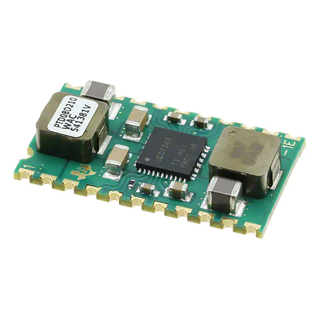
PTD08D210W
www.ti.com
SLTS295B – DECEMBER 2009 – REVISED DECEMBER 2010
DUAL 10-A OUTPUTS, 4.75-V to 14-V INPUT, NON-ISOLATED,
DIGITAL POWERTRAIN™ MODULE
Check for Samples: PTD08D210W
FEATURES
DESCRIPTION
•
•
•
The PTD08D210W is a high-performance dual 10-A
output, non-isolated digital PowerTrain module. This
module is the power conversion section of a digital
power system which incorporates TI's UCD7242
MOSFET/driver IC. The PTD08D210W must be used
in conjunction with a digital power controller such as
the UCD9240, UCD9220 or UCD9110 family. The
PTD08D210W receives control signals from the
digital controller and provides parametric and status
information back to the digital controller. Together,
PowerTrain modules and a digital power controller
form a sophisticated, robust, and easily configured
power management solution.
1
2
•
•
•
•
•
Dual 10-A Outputs
4.75-V to 14-V Input Voltage
Programmable Wide-Output Voltage
(0.7 V to 3.6 V)
Efficiencies up to 96%
Digital I/O
– PWM signal
– Fault Flag (FF)
– Sychronous Rectifier Enable (SRE)
Analog I/O
– Temperature
– Output currrent
Safety Agency Approvals: (Pending)
– UL/IEC/CSA-C22.2 60950-1
Operating Temperature: –40°C to 85°C
APPLICATIONS
•
Digital Power Systems
using UCD9XXX Digital Controllers
Operating from an input voltage range of 4.75 V to
14 V, the PTD08D210W provides step-down power
conversion to a wide range of output voltages from,
0.7 V to 3.6 V. The wide input voltage range makes
the PTD08D210W particularly suitable for advanced
computing and server applications that utilize a
loosely regulated 8-V, 9.6-V or 12-V intermediate
distribution bus. Additionally, the wide input voltage
range increases design flexibility by supporting
operation with tightly regulated 5-V or 12-V
intermediate bus architectures.
The module incorporates output over-current and
temperature monitoring which protects against most
load faults. Output current and module temperature
signals are provided for the digital controller to permit
user defined over-current and over-temperature
warning and fault scerarios.
The module uses single-sided, pin-less surface
mount construction to provide a low profile and
compact footprint. The package is lead (Pb) - free
and RoHS compatible.
1
2
Please be aware that an important notice concerning availability, standard warranty, and use in critical applications of Texas
Instruments semiconductor products and disclaimers thereto appears at the end of this data sheet.
POWERTRAIN is a trademark of Texas Instruments.
PRODUCTION DATA information is current as of publication date.
Products conform to specifications per the terms of the Texas
Instruments standard warranty. Production processing does not
necessarily include testing of all parameters.
Copyright © 2009–2010, Texas Instruments Incorporated
�PTD08D210W
SLTS295B – DECEMBER 2009 – REVISED DECEMBER 2010
www.ti.com
This integrated circuit can be damaged by ESD. Texas Instruments recommends that all integrated circuits be handled with
appropriate precautions. Failure to observe proper handling and installation procedures can cause damage.
ESD damage can range from subtle performance degradation to complete device failure. Precision integrated circuits may be more
susceptible to damage because very small parametric changes could cause the device not to meet its published specifications.
Standard PTD08D210W Application
18
4
17
5
15
7
PWM-A
PWM-B
SRE-A
SRE-B
FF-A
FF-B
Digital
Lines
to/from
Digital
Controller
VOA 22
VI
AGND
PGND
PGND
VOB
AGND
CI2
22 mF
(Required)
GND
ISENSE-B
+
CI1
330 mF
(Recommended)
COA2
330 mF
(Recommended)
PGND 19
ISENSE-A
2
VI
COA1
+
47 mF
(Required)
PGND 20
PTD08D210W
TSENSE
VI
PGND
1
VOA
VOA 21
3
16
14
6
12
13
8
9
VOB 10
VOB 11
GND
COB1
+
47 mF
(Required)
COA2
330 mF
(Recommended)
GND
Analog
Lines
to
Digital
Controller
UDG-09155
2
Submit Documentation Feedback
Copyright © 2009–2010, Texas Instruments Incorporated
Product Folder Link(s): PTD08D210W
�PTD08D210W
www.ti.com
SLTS295B – DECEMBER 2009 – REVISED DECEMBER 2010
ORDERING INFORMATION
For the most current package and ordering information, see the Package Option Addendum at the end of this datasheet, or see
the TI website at www.ti.com.
DATASHEET TABLE OF CONTENTS
DATASHEET SECTION
PAGE NUMBER
ENVIRONMENTAL AND ABSOLUTE MAXIMUM RATINGS
3
ELECTRICAL CHARACTERISTICS TABLE
4
TERMINAL FUNCTIONS
5
TYPICAL CHARACTERISTICS (VI = 12V)
6
TYPICAL CHARACTERISTICS (VI = 5V)
8
TYPICAL APPLICATION SCHEMATIC
10
GRAPHICAL USER INTERFACE VALUES
11
TAPE & REEL AND TRAY DRAWINGS
12
ENVIRONMENTAL AND ABSOLUTE MAXIMUM RATINGS
(Voltages are with respect to GND)
UNIT
VI
Input voltage
TA
Operating temperature range
Over VI range
Treflow
Solder reflow temperature
Surface temperature of module body
Tstg
16
260 (1)
Storage temperature
–55 to 125
Mechanical shock
Per Mil-STD-883D, Method 2002.3, 1 msec, 1/2 sine, mounted
275
Mechanical vibration
Mil-STD-883D, Method 2007.2, 20-2000 Hz
10
Weight
MTBF
(1)
(2)
V
–40 to 85
Reliability
Per Telcordia SR-332, 50% stress, TA = 40°C, ground benign
Flammability
Meets UL94V-O
°C
(2)
G
3.9
grams
13.3
106 Hr
During reflow do not elevate peak temperature of the module or internal components above the stated maximum.
The shipping tray or tape and reel cannot be used to bake parts at temperatures higher than 65°C.
Submit Documentation Feedback
Copyright © 2009–2010, Texas Instruments Incorporated
Product Folder Link(s): PTD08D210W
3
�PTD08D210W
SLTS295B – DECEMBER 2009 – REVISED DECEMBER 2010
www.ti.com
ELECTRICAL CHARACTERISTICS
PTD08D210W
TA= 25°C, FSW= 750kHz, VI= 12 V, VO= 1.2 V, CI1= 330 µF, CI2= 22 µF ceramic, CO1= 47 µF ceramic, CO2= 330 µF, IO= IO(max),
single output (unless otherwise stated)
PARAMETER
TEST CONDITIONS
PTD08D210W
MIN
IO
Output current
Over VO range
VI
Input voltage range
VOADJ
Output voltage adjust range
Efficiency
h
25°C, natural convection
10
A
Over IO range
4.75
14
V
Over IO range
0.7
3.6 (1)
V
IO = 10 A,
fs = 750 kHz
VO Ripple (peak-to-peak)
20-MHz bandwidth
IB
Bias current
PWM & SRE to AGND
VIH
High-level input voltage
VIL
Low-level input voltage
VO = 3.3 V
92.8%
VO = 2.5 V
91.4%
VO = 1.8 V
89.1%
VO = 1.5 V
87.7%
VO = 1.2 V
85.6%
VO = 1.0 V
84.0%
11
Standby
SRE & PWM input levels
VOL
Frequency range
500 (1)
Pulse width limits
20
Accuracy, -40°C ≤ TA ≤ 85°C
-5
ILIM
Gain, 3A ≤ IO ≤ 10A
188
0
Offset, IO = 0A, VO = 1.2V
3.3
CO
External output capacitance
Ceramic
Equivalent series resistance (non-ceramic)
(1)
(2)
(3)
(4)
(5)
(6)
4
0.6
22
(3)
47
(4)
Nonceramic
Ceramic
1 (6)
V
A
3.5
V
200
212
mV/A
0.3
0.76
10
Nonceramic
°C
mV
15 (2)
0.15
Capacitance Value
°C
720
0
Range
External input capacitance
125
mV/°C
Output Impedance
CI
kHz
10
Low-level output voltage, IFAULT = 4mA
Overcurrent threshold; Reset, followed by auto-recovery
IOUT output
1000
5
Slope
2.7
V
ns
-40
High-level output voltage, IFAULT = 4mA
FAULT output
mA
5.5
0.8
Offset, TA = 25°C
VOH
mVPP
6
2.0
Range
TEMP output
MAX
0
VOPP
PWM input
TYP
UNIT
330
(3)
330
(4)
V
kΩ
µF
5000 (5)
µF
mΩ
When operating at 12V input and 500kHz, VO is limited to ≤ 2.0V.
The current limit threshold is the sum of IO and the peak inductor ripple current.
A 22 µF ceramic input capacitor is required for proper operation. An additional 330 µF bulk capacitor rated for a minimum of 500mA rms
of ripple current is recommended. When operating at frequencies > 500kHz the 22 µF ceramic capacitor is only recommended. Refer to
the UCD9240 controller datasheet and user interface for application specific capacitor specifications.
A 47 µF ceramic output capacitor is required for basic operation. An additional 330 µF bulk capacitor is recommended for improved
transient response. Refer to the UCD9240 controller datasheet and user interface for application specific capacitor specifications.
5,000 µF is the calculated maximum output capacitance given a 1V/msec output voltage rise time. Additional capacitance or increasing
the output voltage rise rate may trigger the overcurrent threshold at start-up. Refer to the UCD9240 controller datasheet and user
interface for application specific capacitor specifications.
This is the minimum ESR for all non-ceramic output capacitance. Refer to the UCD9240 controller datasheet and user interface for
application specific capacitor specifications.
Submit Documentation Feedback
Copyright © 2009–2010, Texas Instruments Incorporated
Product Folder Link(s): PTD08D210W
�PTD08D210W
www.ti.com
SLTS295B – DECEMBER 2009 – REVISED DECEMBER 2010
TERMINAL FUNCTIONS
TERMINAL
NAME
VI
PGND
NO.
1, 2
DESCRIPTION
The positive input voltage power node to the module, which is referenced to common GND.
3, 8, 9, 19,
The common ground connection for the VI and VO power connections.
20
VOA
21, 22
The regulated positive power A output with respect to GND.
VOB
10, 11
The regulated positive power B output with respect to GND.
ISENSE-A
14
Current sense A output. The voltage level on this pin represents the average output current of the module.
ISENSE-B
6
Current sense B output. The voltage level on this pin represents the average output current of the module.
PWM-A
18
This is the PWM A input pin. It is a high impedance digital input that accepts 3.3-V or 5-V logic level signals up to
1 MHz.
PWM-B
4
This is the PWM B input pin. It is a high impedance digital input that accepts 3.3-V or 5-V logic level signals up to
1 MHz.
FF-A
15
Current limit fault flag A. The Fault signal is a 3.3-V digital output which is latched high after an over-current
condition. The Fault is reset after a complete PWM cycle without an over-current condition (falling edge of the
PWM).
FF-B
7
Current limit fault flag A. The Fault signal is a 3.3-V digital output which is latched high after an over-current
condition. The Fault is reset after a complete PWM cycle without an over-current condition (falling edge of the
PWM).
SRE-A
17
Synchronous Rectifier Enable A. This pin is a high impedance digital input. A 3.3 V or 5 V logic level signals is used
to enable the synchronous rectifier switch. When this signal is high, the module will source and sink output current.
When this signal is low, the module will only source current.
SRE-B
5
Synchronous Rectifier Enable B. This pin is a high impedance digital input. A 3.3 V or 5 V logic level signals is used
to enable the synchronous rectifier switch. When this signal is high, the module will source and sink output current.
When this signal is low, the module will only source current.
AGND
12, 13
TSENSE
16
Thermal
Pad
Analog ground return. It is the 0 Vdc reference for the control inputs.
Temperature sense output. The voltage level on this pin represents the temperature of the module.
This pad is electrically connected to PGND and is the primary thermal conduction cooling path for the module. This
pad should be soldered to a grounded copper pad on the host board. For optimum cooling performance, the
grounded copper pad should also be tied with multiple vias to the host board internal ground plane. See the Land
Pattern drawing for package EFS for recommended pad dimensions.
XX
XX
VI
1
VI
2
PGND
3
PWM-B
4
BOTTOM VIEW
1
TOP VIEW
22
VO-A
22
VO-A
21
2
21
PGND
20
3
PGND
19
4
PWM-A
18
5
20
19
SRE-B
5
ISENSE-B
6
17
SRE-A
17
6
FF-B
7
16
TSENSE
16
7
PGND
8
FF-A
15
PGND
VO-B
VO-B
9
10
11
18
15
8
Thermal
Pad
14
ISENSE-A
14
13
AGND
13
10
AGND
12
11
12
9
Submit Documentation Feedback
Copyright © 2009–2010, Texas Instruments Incorporated
Product Folder Link(s): PTD08D210W
5
�PTD08D210W
SLTS295B – DECEMBER 2009 – REVISED DECEMBER 2010
www.ti.com
TYPICAL CHARACTERISTICS (VI = 12 V)
. (1) (2)
100
100
100
VO = 3.3 V
VO = 1.8 V
90
VO = 1.2 V
VO = 0.8 V
70
60
80
VO = 1.8 V
VO = 1.2 V
70
VO = 0.8 V
60
VI = 12 V
fSW = 500 kHz
4
6
8
10
4
6
6
8
VO = 1.2 V
VO = 1.8 V
2.0
VO = 2.5 V
1.5
VO = 3.3 V
1.0
VO = 1.2 V
4
6
8
10
0
2
4
6
8
VO = 1.2 V
0
10
8
200 LFM
60
100 LFM
50
Natural Convection
400 LFM
70
200 LFM
60
100 LFM
50
40
Natural Convection
30
VI = 12 V
fSW = 500 kHz
0
1
200 LFM
60
100 LFM
50
40
Natural Convection
2
3
4
5
VI = 12 V
fSW = 1 MHz
PD(VOA)+PD(VOB)
20
20
5
70
30
VI = 12 V
fSW = 750 kHz
PD(VOA)+PD(VOB)
20
10
80
TA – Ambient Temperature – °C
TA – Ambient Temperature – °C
70
Figure 7. Safe Operating Area
6
90
80
80
PD – Total Power Dissipation – W
4
400 LFM
400 LFM
4
2
Figure 6. Power Dissipation
90
90
3
1.0
IO – Output Current – A
Figure 5. Power Dissipation
2
VO = 3.3 V
VO = 0.8 V
Figure 4. Power Dissipation
PD(VOA)+PD(VOB)
1.5
0
IO – Output Current – A
30
VO = 2.5 V
VO = 0.8 V
IO – Output Current – A
40
VO = 1.8 V
2.0
0.5
0.5
0
2
VI = 12 V
fSW = 1 MHz
2.5
PD – Power Dissipation – W
1.0
10
3.0
VI = 12 V
fSW = 750 kHz
2.5
VO = 1.8 V
1
4
Figure 3. Efficiency
2.0
0
2
Figure 2. Efficiency
0
TA – Ambient Temperature – °C
0
Figure 1. Efficiency
VO = 0.8 V
6
10
IO – Output Current – A
0.5
(2)
8
IO – Output Current – A
PD – Power Dissipation – W
PD – Power Dissipation – W
2
3.0
0
60
IO – Output Current – A
VI = 12 V
fSW = 500 kHz
1.5
VO = 0.8 V
40
0
3.0
2.5
VO = 1.2 V
VI = 12 V
fSW = 1 MHz
40
2
VO = 1.8 V
70
VI = 12 V
fSW = 750 kHz
40
0
80
50
50
50
(1)
h – Efficiency – %
h – Efficiency – %
80
VO = 3.3 V
VO = 2.5 V
90
90
h – Efficiency – %
VO = 2.5 V
0
1
2
3
4
PD – Total Power Dissipation – W
PD – Total Power Dissipation – W
Figure 8. Safe Operating Area
Figure 9. Safe Operating Area
5
The electrical characteristic data (Figure 1 through Figure 6) has been developed from actual products tested at 25°C. This data is
considered typical for the converter.
The temperature derating curves (Figure 7 through Figure 9) represent the conditions at which internal components are at or below the
manufacturer's maximum operating temperatures. Derating limits apply to modules soldered directly to a 100-mm x 100-mm,
double-sided PCB with 2-oz. copper. See the Safe Operating Area application section of this datasheet.
Submit Documentation Feedback
Copyright © 2009–2010, Texas Instruments Incorporated
Product Folder Link(s): PTD08D210W
�PTD08D210W
www.ti.com
SLTS295B – DECEMBER 2009 – REVISED DECEMBER 2010
TYPICAL CHARACTERISTICS (VI = 5 V)
. (1) (2)
100
100
VO = 3.3 V
VO = 1.8 V
VO = 0.8 V
VO = 1.2 V
70
60
80
VO = 1.8 V
VO = 0.8 V
70
VO = 1.2 V
60
50
50
6
8
10
4
6
8
2.0
1.5
1.0
VO = 1.8 V
VO = 2.5 V
2.0
1.5
1.0
VO = 1.8 V
0.5
4
6
2.0
1.5
1.0
VO = 1.8 V
0.5
VO = 1.2 V
VO = 1.2 V
VO = 0.8 V
0
8
VO = 3.3 V
VO = 2.5 V
VO = 0.8 V
VO = 0.8 V
2
VI = 5 V
fSW = 1 MHz
2.5
VO = 3.3 V
PD – Power Dissipation – W
VO = 2.5 V
0
10
2
4
6
8
0
10
0
2
4
6
8
IO – Output Current – A
IO – Output Current – A
IO – Output Current – A
Figure 13. Power Dissipation
Figure 14. Power Dissipation
Figure 15. Power Dissipation
90
400 LFM
400 LFM
80
TA – Ambient Temperature – °C
80
70
200 LFM
60
100 LFM
50
40
Natural Convection
200 LFM
60
VI = 5 V
fSW = 500 kHz
PD(VOA)+PD(VOB)
100 LFM
50
40
Natural Convection
1
2
3
4
5
PD – Total Power Dissipation – W
Figure 16. Safe Operating Area
0
1
2
3
4
PD – Total Power Dissipation – W
Figure 17. Safe Operating Area
70
200 LFM
60
100 LFM
50
40
Natural Convection
30
VI = 5 V
fSW = 750 kHz
PD(VOA)+PD(VOB)
20
400 LFM
80
70
30
30
10
90
TA – Ambient Temperature – °C
90
10
3.0
VI = 5 V
fSW = 750 kHz
2.5
0
TA – Ambient Temperature – °C
8
Figure 12. Efficiency
VO = 1.2 V
(2)
6
Figure 11. Efficiency
VO = 3.3 V
0
4
Figure 10. Efficiency
3.0
20
2
IO – Output Current – A
0.5
(1)
0
10
IO – Output Current – A
PD – Power Dissipation – W
PD – Power Dissipation – W
2
IO – Output Current – A
VI = 5 V
fSW = 500 kHz
0
60
40
0
3.0
2.5
VO = 1.2 V
70
VI = 5 V
fSW = 1 MHz
40
4
VO = 1.8 V
VO = 0.8 V
VI = 5 V
fSW = 750 kHz
40
2
80
50
VI = 5 V
fSW = 500 kHz
0
VO = 3.3 V
90
h – Efficiency – %
h – Efficiency – %
80
VO = 2.5 V
VO = 3.3 V
90
90
h – Efficiency – %
100
VO = 2.5 V
VO = 2.5 V
VI = 5 V
fSW = 1 MHz
PD(VOA)+PD(VOB)
5
20
0
1
2
3
4
5
PD – Total Power Dissipation – W
Figure 18. Safe Operating Area
The electrical characteristic data (Figure 10 through Figure 15) has been developed from actual products tested at 25°C. This data is
considered typical for the converter.
The temperature derating curves (Figure 16 through Figure 18) represent the conditions at which internal components are at or below
the manufacturer's maximum operating temperatures. Derating limits apply to modules soldered directly to a 100-mm x 100-mm,
double-sided PCB with 2-oz. copper. See the Safe Operating Area application section of this datasheet.
Submit Documentation Feedback
Copyright © 2009–2010, Texas Instruments Incorporated
Product Folder Link(s): PTD08D210W
7
�PTD08D210W
SLTS295B – DECEMBER 2009 – REVISED DECEMBER 2010
www.ti.com
TYPICAL CHARACTERISTICS
CURRENT SENSE OUTPUT
vs
OUTPUT CURRENT
CURRENT SENSE OUTPUT
vs
OUTPUT CURRENT
1.2
1.0
0.8
0.6
0.4
0.2
VTSENSE – Temperature Sense Output Voltage – V
1.6
1.4
0
VI = 5 V
1.8
1.6
1.4
1.2
1.0
0.8
0.6
0.4
0.2
0
0
8
2.0
2.0
VI = 12 V
1.8
VISENSE – Current Sense Output Voltage – V
VISENSE – Current Sense Output Voltage – V
2.0
TEMPERATURE SENSE
vs
JUNCTION TEMPERATURE
2
4
6
8
10
0
2
4
6
8
10
1.8
1.6
1.4
1.2
1.0
0.8
0.6
0.4
0.2
0
–50
–25
0
25
50
75
100
IO – Output Current – A
IO – Output Current – A
TJ – Junction Temperature – °C
Figure 19.
Figure 20.
Figure 21.
Submit Documentation Feedback
125
150
Copyright © 2009–2010, Texas Instruments Incorporated
Product Folder Link(s): PTD08D210W
�PTD08D210W
www.ti.com
SLTS295B – DECEMBER 2009 – REVISED DECEMBER 2010
APPLICATION INFORMATION
Determining the Safe Operating Area
3.0
2.5
PD – Power Dissipation – W
The Safe Operating Area (SOA) curves for the
PTD08D210W are determined by the total power
dissipation of the module, the maximum ambient
temperature, and the minimum available airflow of the
application. Operation below the application airflow
curve is considered a thermally safe design. For a
given SOA, refer to the Power Dissipation curves for
the same input voltage and switching frequency to
determine each output's power dissipation. Add the
power dissipation of VOA and VOB to get the total power
dissipation. The total power dissipation can then be
used to determine the safe operating area for the
application.
VI = 12 V
fSW = 750 kHz
VO = 1.8 V
2.0
VO = 2.5 V
1.5
VO = 3.3 V
1.0
VO = 1.2 V
0.5
VO = 0.8 V
0
0
2
4
6
8
10
IO – Output Current – A
90
400 LFM
TA – Ambient Temperature – °C
80
70
60
200 LFM
50
For example, consider an application operating from a
12-V input and a 750-kHz switching frequency,
requiring 1.2 V @ 10 A and 3.3 V @ 6 A outputs. In
order to determine the safe operating area the power
dissipation for each of the outputs must first be
determined. Using the VI = 12 V, fSW = 750 kHz Power
Dissipation graph, the power dissipation for the 1.2 V
@ 10 A output is 2 W and the power dissipation for the
3.3 V @ 6 A output is 1.5 W. Adding the power
dissipation for both outputs results in a total power
dissipation of 3.5 W. The safe operating area can then
be determined using the VI = 12V, fSW = 750 kHz SOA
graph, the amount of airflow of the application and the
3.5-W total power dissipation. At 3.5 W and 400 LFM,
the application can operate up to 85°C, but when no
airflow is available the maximum ambient temperature
is limited to less than 71°C.
100 LFM
40
Natural Convection
30
VI = 12 V
fSW = 750 kHz
PD(VOA)+PD(VOB)
20
0
1
2
3
3.5
4
5
PD – Total Power Dissipation – W
NOTE
•
•
Graphs above have been replicated from the Typical Characteristics section for this example
The maximum output current for either output must not exceed 10 A.
Submit Documentation Feedback
Copyright © 2009–2010, Texas Instruments Incorporated
Product Folder Link(s): PTD08D210W
9
�PTD08D210W
SLTS295B – DECEMBER 2009 – REVISED DECEMBER 2010
www.ti.com
Digital Power
Figure 22 shows the UCD9220 power supply controller working with a single PTD08D210W, dual-output module
regulating two independent power supplies. The loop for each power supply is created by the respective voltage
outputs feeding into the Error ADC differential inputs, and completed by DPWM outputs feeding the
PTD08D210W module.
VIN
5
3
35
33
34
V33A
BPCap
Vin/Iin
V33FB
4
V33D
41
+3.3 V
FLT-1A
SRE-1A
CS-1A
FAULT-1B
26
27
28
29
30
31
43
44
45
UCD9220
SRE-2A
TMUX-0
CS-2A
PowerGood
FAULT-3A
TCK
DPWM-3A
SRE-3A
TDO/SYNC-OUT
TDI/SYNC-IN
CS-3A
TMS
Temp
6
VOA 22
VOA
VOUT-A
21
18 PWM-A
PGND 20
9
17 SRE-A
PGND 19
42
7
14 Isense-A
PTD08D210W
7
FF-B
VOB 11
2
4
PWM-B
VOB 10
8
5
SRE-B
PGND
8
14
6
Isense-B
PGND
9
13
18
VOUT-B
15
3
AGND AGND Tsense
12
13
16
25
16
17
1
46
37
TRST
EAP1
ADDR-0
EAN1
ADDR-1
Vtrack
ADCref
VIN
12
TMUX-1
EAP2
36
48
DPWM-2A
GPIO-2
PowerPad
24
FAULT-2A
GPIO-1
VIN
PGND
EAN2
38
39
40
49
22
23
PMBus-CNTL
DGND1
21
CS-1B
PMBus-Alert
AGND2
20
32
19
SRE-1B
PMBus-Data
47
11
DPWM-1B
PMBus-CLK
AGND1
10
2
15 FF-A
DPWM-1A
RESET
1
UDG-09173
Figure 22. Typical Dual-Output Application Schematic
Note: A low dropout linear regulator such as the TI TPS715A33 can provide the 3.3-V bias power to the UCD9220.
10
Submit Documentation Feedback
Copyright © 2009–2010, Texas Instruments Incorporated
Product Folder Link(s): PTD08D210W
�PTD08D210W
www.ti.com
SLTS295B – DECEMBER 2009 – REVISED DECEMBER 2010
Figure 23 shows the UCD9220 power supply controller working with a single PTD08D210W power module. The
dual outputs of the PTD08D210W have been paralleled, allowing up to 20A of output current. When operating
the PTD08D210W in parallel configuration the dual inputs must be tied together and driven from a single output
of the digital power controller. Multiple PTD08D210W modules must not be paralleled.
VIN
3
35
33
34
V33A
BPCap
Vin/Iin
V33FB
4
V33D
41
+3.3 V
RESET
FLT-1A
SRE-1A
CS-1A
FAULT-1B
27
28
29
30
31
43
44
45
UCD9220
SRE-2A
TMUX-0
CS-2A
PowerGood
FAULT-3A
TCK
DPWM-3A
SRE-3A
TDO/SYNC-OUT
TDI/SYNC-IN
CS-3A
TMS
Temp
VOA 22
VOA
21
VOUT
12
9
18 PWM-A
PGND 20
17 SRE-A
PGND 19
42
7
14 Isense-A
PTD08D210W
7
FF-B
VOB 11
2
4
PWM-B
VOB 10
8
5 SRE-B
PGND
9
14
6
PGND
8
13
18
Isense-B
15
3
AGND AGND Tsense
12
13
16
25
16
17
1
46
37
TRST
EAP1
ADDR-0
EAN1
ADDR-1
Vtrack
ADCref
VIN
6
TMUX-1
EAP2
36
48
DPWM-2A
GPIO-2
PowerPad
26
FAULT-2A
GPIO-1
VIN
PGND
EAN2
38
39
40
49
24
PMBus-CNTL
DGND1
22
23
CS-1B
PMBus-Alert
AGND2
20
21
SRE-1B
PMBus-Data
32
19
47
11
DPWM-1B
PMBus-CLK
AGND1
10
2
15 FF-A
DPWM-1A
5
1
UDG-01001
Figure 23. Typical Paralleled-Output Application Schematic
Note 1: A low dropout linear regulator such as the TI TPS715A33 can provide the 3.3-V bias power to the UCD9220.
Note 2: An OR-gate such as the TI 74LVC1G32 should be used to sense a fault signal on either FF-A or FF-B.
Submit Documentation Feedback
Copyright © 2009–2010, Texas Instruments Incorporated
Product Folder Link(s): PTD08D210W
11
�PTD08D210W
SLTS295B – DECEMBER 2009 – REVISED DECEMBER 2010
www.ti.com
UCD9240 Graphical User Interface (GUI)
When using the UCD92x0 digital controller along with digital PowerTrain modules to design a digital power
system, several internal parameters of the modules are required to run the Fusion Digital Power Designer GUI.
See the plant parameters below for the PTD08D210W digital PowerTrain modules.
Table 1. PTD08D210W Plant Parameters
PTD08D210W Plant Parameters
L (µH)
DCR (mΩ)
RDS(on)-high (mΩ)
RDS(on)-low (mΩ)
0.47
2.6
15.5
6.5
Internal output capacitance is present on the digital PowerTrain modules themselves. When using the GUI
interface this capacitance information must be included along with any additional external capacitance. See the
capacitor parameters below for the PTD08D210W digital PowerTrain modules.
Table 2. PTD08D210W Capacitor Parameters
PTD08D210W Capacitor Parameters
12
C (µF)
ESR (mΩ)
ESL (nH)
Quantity
47
1.5
2.5
1
Submit Documentation Feedback
Copyright © 2009–2010, Texas Instruments Incorporated
Product Folder Link(s): PTD08D210W
�PTD08D210W
www.ti.com
SLTS295B – DECEMBER 2009 – REVISED DECEMBER 2010
TAPE & REEL
Submit Documentation Feedback
Copyright © 2009–2010, Texas Instruments Incorporated
Product Folder Link(s): PTD08D210W
13
�PTD08D210W
SLTS295B – DECEMBER 2009 – REVISED DECEMBER 2010
www.ti.com
TRAY
14
Submit Documentation Feedback
Copyright © 2009–2010, Texas Instruments Incorporated
Product Folder Link(s): PTD08D210W
�PTD08D210W
www.ti.com
SLTS295B – DECEMBER 2009 – REVISED DECEMBER 2010
REVISION HISTORY
Changes from Revision A (FEBRUARY 2010) to Revision B
•
Page
Added Caution regarding paralleling multiple modules. ..................................................................................................... 11
Submit Documentation Feedback
Copyright © 2009–2010, Texas Instruments Incorporated
Product Folder Link(s): PTD08D210W
15
�PACKAGE OPTION ADDENDUM
www.ti.com
19-Dec-2019
PACKAGING INFORMATION
Orderable Device
Status
(1)
Package Type Package Pins Package
Drawing
Qty
Eco Plan
Lead/Ball Finish
MSL Peak Temp
(2)
(6)
(3)
Op Temp (°C)
Device Marking
(4/5)
PTD08D210WAC
ACTIVE
DIP MODULE
EFS
22
36
RoHS (In
Work) & Green
(In Work)
Call TI
Level-3-260C-168 HR
-40 to 85
PTD08D210WACT
ACTIVE
DIP MODULE
EFS
22
250
RoHS (In
Work) & Green
(In Work)
Call TI
Level-3-260C-168 HR
-40 to 85
(1)
The marketing status values are defined as follows:
ACTIVE: Product device recommended for new designs.
LIFEBUY: TI has announced that the device will be discontinued, and a lifetime-buy period is in effect.
NRND: Not recommended for new designs. Device is in production to support existing customers, but TI does not recommend using this part in a new design.
PREVIEW: Device has been announced but is not in production. Samples may or may not be available.
OBSOLETE: TI has discontinued the production of the device.
(2)
RoHS: TI defines "RoHS" to mean semiconductor products that are compliant with the current EU RoHS requirements for all 10 RoHS substances, including the requirement that RoHS substance
do not exceed 0.1% by weight in homogeneous materials. Where designed to be soldered at high temperatures, "RoHS" products are suitable for use in specified lead-free processes. TI may
reference these types of products as "Pb-Free".
RoHS Exempt: TI defines "RoHS Exempt" to mean products that contain lead but are compliant with EU RoHS pursuant to a specific EU RoHS exemption.
Green: TI defines "Green" to mean the content of Chlorine (Cl) and Bromine (Br) based flame retardants meet JS709B low halogen requirements of


 工商网监
湘ICP备2023018690号
工商网监
湘ICP备2023018690号
