PTH03000W —3.3-V Input
6-A, 3.3-V Input Non-Isolated
Wide-Output Adjust Power Module
SLTS200C – MAY 2003 – REVISED DECEMBER 2003
Features
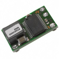
NOMINAL SIZE =
0.75 in x 0.5 in
(19,05 mm x 12,7 mm)
• Up to 6-A Output Current
• 3.3 V Input Voltage
• Wide-Output Voltage Adjust
(0.9 V to 2.5 V)
• Efficiencies up to 95 %
• 115 W/in³ Power Density
• On/Off Inhibit
• Under-Voltage Lockout
•
•
•
•
•
Output Current Limit
Over-Temperature Protection
Operating Temp: –40 to +85 °C
Surface Mount Package
Safety Agency Approvals (Pending):
UL 1950, CSA 22.2 950, EN60950
& VDE
Description
Pin Configuration
The PTH03000 series of non-isolated
power modules are small in size and high
on performance. Using double-sided surface mount construction and synchronous
rectification technology, these regulators
deliver up to 6 A of output current while
occupying a PCB area of about half the
size of a standard postage stamp. They
are an ideal choice for applications where
space, performance and cost are important design constraints.
The series operates from an input
voltage of 3.3 V to provide step-down
power conversion to any output voltage
over the range, 0.9 V to 2.5 V. The output voltage of the PTH03000W is set
within this range using a single resistor.
Operating features include an on/off
inhibit, output voltage adjust (trim), an
output current limit, and over-temperature
protection.
Target applications include telecom,
industrial, and general purpose circuits,
including low-power dual-voltage systems
that use a DSP, microprocessor, or ASIC.
Package options include both throughhole and surface mount configurations.
Pin
1
2
3
4
5
* Denotes negative logic:
Open
= Output On
Ground = Output Off
Standard Application
Rset = Required to set the output voltage to a value
higher than 0.9 V (see spec. table for values)
Cin = Required 100 µF capacitor
Cout = Optional 100 µF capacitor
1
VIN
2
PTH03000W
(Top View)
3
CIN
100 µF
(Required)
VOUT
5
4
RSET
1 %, 0.1 W
(Required)
COUT
100 µF
Electrolytic
(Optional)
Inhibit
GND
For technical support and further information visit http://power.ti.com
Function
GND
Vin
Inhibit *
Vo Adjust
Vout
GND
�PTH03000W —3.3-V Input
6-A, 3.3-V Input Non-Isolated
Wide-Output Adjust Power Module
SLTS200C – MAY 2003 – REVISED DECEMBER 2003
Ordering Information
Output Voltage (PTH03000Hxx)
Package Options (PTH03000xHH) (1)
Code
W
Code
Voltage
0.9 V – 2.5 V (Adjust)
AH
AS
Description
Pkg Ref.
Horiz. T/H
SMD, Standard (3)
(2)
(EUS)
(EUT)
Notes: (1) Add “T” to end of part number for tape and reel on SMD packages only.
(2) Reference the applicable package reference drawing for the dimensions and PC board layout
(3) “Standard” option specifies 63/37, Sn/Pb pin solder material.
Pin Descriptions
Vin: The positive input voltage power node to the module, which is referenced to common GND.
Vout: The regulated positive power output with respect
to the GND node.
GND: This is the common ground connection for the
‘Vin’ and ‘Vout’ power connections. It is also the 0 VDC
reference for the ‘Inhibit’ and ‘Vo Adjust’ control inputs.
Inhibit: The Inhibit pin is an open-collector/drain negative
logic input that is referenced to GND. Applying a lowlevel ground signal to this input disables the module’s
output and turns off the output voltage. When the Inhibit
control is active, the input current drawn by the regulator
is significantly reduced. If the Inhibit pin is left opencircuit, the module will produce an output whenever a
valid input source is applied.
Vo Adjust: A 0.1 W 1 % resistor must be directly connected
between this pin and the GND pin to set the output voltage
to a value higher than 0.9 V. The temperature stability
of the resistor should be 100 ppm/°C (or better). The set
point range for the output voltage is from 0.9 V to 2.5 V.
The resistor required for a given output voltage may be
calculated from the following formula. If left open circuit,
the output voltage will default to its lowest value. For
further information on output voltage adjustment, consult
the related application note.
Rset
= 10 kΩ ·
0.891 V
Vout – 0.9 V
– 4.99 kΩ
The specification table gives the preferred resistor values
for a number of standard output voltages.
For technical support and further information visit http://power.ti.com
�PTH03000W —3.3-V Input
6-A, 3.3-V Input Non-Isolated
Wide-Output Adjust Power Module
SLTS200C– MAY 2003 – REVISED DECEMBER 2003
Environmental & Absolute Maximum Ratings
Characteristics
Symbols
Conditions
Min
Typ
Max
Units
Operating Temperature Range
Solder Reflow Temperature
Storage Temperature
Over Temperature Protection
Mechanical Shock
Ta
Treflow
Ts
OTP
Over Vin Range
Surface temperature of module body or pins
—
IC junction temperature
Per Mil-STD-883D, Method 2002.3
1 msec, ½ sine, mounted
Mil-STD-883D, Method 2007.2
20-2000 Hz
–40 (i)
—
–40
—
—
—
150
500
+85
235 (ii)
+125
—
—
°C
°C
°C
°C
G’s
—
20
—
G’s
—
2
—
grams
Mechanical Vibration
Weight
Flammability
—
—
Meets UL 94V-O
Notes: (i) During reflow of SMD package version do not elevate peak temperature of the module, pins or internal components above the stated maximum.
Electrical Specifications
Unless otherwise stated, T a =25 °C, V in =3.3 V, Vo =2 V, C in =100 µF, C out =0 µF, and Io =Iomax
Characteristics
Symbols
Conditions
Output Current
Io
0.9 V ≤ Vo ≤ 2.5 V,
Input Voltage Range
Set-Point Voltage Tolerance
Temperature Variation
Line Regulation
Load Regulation
Total Output Variation
Vin
Vo tol
∆Regtemp
∆Regline
∆Regload
∆Regtot
Over Io range
Efficiency
η
Vo Ripple (pk-pk)
Transient Response
Vr
Current Limit
Under-Voltage Lockout
ttr
∆Vtr
Ilim
UVLO
Inhibit Control (pin 3)
Input High Voltage
Input Low Voltage
Input Low Current
VIH
VIL
IIL
Standby Input Current
Switching Frequency
External Input Capacitance
External Output Capacitance
Iin inh
ƒs
Cin
Cout
Reliability
MTBF
Min
Ta =60 °C, 200 LFM airflow
Ta =25 °C, natural convection
–40 °C 2800 mA
>2400mA
7×8
6.3×9.8
7.3×5.7
1
1
1
≤3
≤2
≤2
10SVP120M
16SPS100M
10TPE220ML
10 V
10 V
100 µF
220 µF
0.100 Ω
0.100 Ω
>1090 mA
>1414 mA
7.3L
×4.3W ×4.1H
1
1
≤3
≤3
TPSD107M010R0100
TPSV227M010R0100
Kemet
T520, Poly-Alum (SMD)
T495,Tantalum (SMD)
A700-Poly-Alum. (SMD)
10 V
10 V
6.3 V
100 µF
100 µF
100 µF
0.080 Ω
0.100 Ω
0.018 Ω
1200 mA
>1100 mA
2900 mA
7.3L ×5.7W
×4.0H
1
1
1
≤4
≤4
≤2
T520D107M010AS
T495X107M010AS
A700D107M006AT
Vishay-Sprague
594D, Tantalum (SMD)
595D, Tantalum (SMD)
94SA, Os-con (Radial)
10 V
10 V
10 V
150 µF
120 µF
100 µF
0.090 Ω
0.140 Ω
0.030 Ω
1100 mA
>1000 mA
2670 mA
7.3L
×6.0W ×4.1H
8×10.5
1
1
1
≤4
≤4
≤2
594D157X0010C2T
595D127X0010D2T
94SA107X0010EBP
Kemet, Ceramic X5R (SMD)
16 V
6.3 V
10
47
0.002 Ω
0.002 Ω
—
1210 case
3225 mm
1
2 [1]
≤5
≤2
C1210C106M4PAC
C1210C476K9PAC
Murata, Ceramic X5R (SMD)
6.3 V
6.3 V
16 V
16 V
100
47
22
10
0.002 Ω
—
1210 case
3225 mm
1
2 [1]
5
1 [2]
≤1
≤2
≤3
≤5
GRM32ER60J107M
GRM32ER60J476M
GRM32ER61C226K
GRM32DR61C106K
TDK, Ceramic X5R (SMD)
6.3 V
6.3 V
16 V
16 V
100
47
22
10
0.002 Ω
—
1210 case
3225 mm
1
2 [1]
5
1 [2]
≤1
≤2
≤3
≤5
C3225X5R0J107MT
C3225X5R0J476MT
C3225X5R1C226MT
C3225X5R1C106MT
AVX, Tantalum
TPS (SMD)
Vendor Number
[1] A total capacitance of 94 µF is acceptable based on the combined ripple current rating.
[2] A ceramic capacitor may be used to complement electrolytic types at the input to further reduce high-frequency ripple current.
For technical support and further information visit http://power.ti.com
�Application Notes
PTH03000W
Adjusting the Output Voltage of the PTH03000W
Wide-Output Adjust Power Modules
The Vo Adjust control (pin 4) sets the output voltage of
the PTH03000Wproduct. The adjustment range is
from 0.9 V to 2.5 V. The adjustment method requires
the addition of a single external resistor, Rset, that must
be connected directly between the Vo Adjust and GND
pins 1. Table 2-1 gives the preferred value of the external
resistor for a number of standard voltages, along with the
actual output voltage that this resistance value provides.
For other output voltages the value of the required resistor
can either be calculated using the following formula, or
simply selected from the range of values given in Table 2-2.
Figure 2-1 shows the placement of the required resistor.
Rset
= 10 kΩ ·
0.891 V
Vout – 0.9 V
– 4.99 kΩ
Table 2-1; Preferred Values of Rset for Standard Output Voltages
Vout (Standard)
Rset (Pref’d Value)
2.5 V
2V
1.8 V
1.5 V
1.2 V
1V
0.9 V
576 Ω
3.09 kΩ
4.87 kΩ
9.76 kΩ
24.3 kΩ
82.5 kΩ
Open
Vout (Actual)
2.501V
2.003 V
1.804 V
1.504 V
1.204 V
1.002 V
0.9 V
4
PTH03000W
Inhibit
CIN
100µF
(Required)
3
VO
5
VOUT
GND
1
RSET
0.1 W, 1 %
+
VIN
0.900
0.925
0.950
0.975
1.000
1.025
1.050
1.075
1.100
1.125
1.150
1.175
1.200
1.225
1.250
1.275
1.300
1.325
1.350
1.375
1.400
1.425
1.450
1.475
Rset
Open
351 kΩ
173 kΩ
114 kΩ
84.1 kΩ
66.3 kΩ
54.4 kΩ
45.9 kΩ
39.6 kΩ
34.6 kΩ
30.7 kΩ
27.4 kΩ
24.7 kΩ
22.4 kΩ
20.5 kΩ
18.8 kΩ
17.3 kΩ
16.0 kΩ
14.8 kΩ
13.8 kΩ
12.8 kΩ
12.0 kΩ
11.2 kΩ
10.5 kΩ
Va Req’d
1.50
1.55
1.60
1.65
1.70
1.75
1.80
1.85
1.90
1.95
2.00
2.05
2.10
2.15
2.20
2.25
2.30
2.35
2.40
2.45
2.50
Rset
9.86 kΩ
8.72 kΩ
7.74 kΩ
6.89 kΩ
6.15 kΩ
5.49 kΩ
4.91 kΩ
4.39 kΩ
3.92 kΩ
3.50 kΩ
3.11 kΩ
2.76 kΩ
2.44 kΩ
2.14 kΩ
1.86 kΩ
1.61 kΩ
1.37 kΩ
1.15 kΩ
950 Ω
758 Ω
579 Ω
2. Never connect capacitors from Vo Adjust to either GND or
Vout. Any capacitance added to the Vo Adjust pin will affect
the stability of the regulator.
V O Adj
2
Va Req’d
Notes:
1. Use a 0.1 W resistor. The tolerance should be 1 %,
with a temperature stability of 100 ppm/°C (or better).
Place the resistor as close to the regulator as possible.
Connect the resistor directly between pins 4 and 1
using dedicated PCB traces.
Figure 2-1; Vo Adjust Resistor Placement
VIN
Table 2-2; Output Voltage Set-Point Resistor Values
COUT
100µF
(Optional)
+
Inhibit
GND
For technical support and further information visit http://power.ti.com
GND
�Application Notes
PTH03000 & PTH05000 Series
Power-Up Characteristics
When configured per their standard application, the
PTH03000 and PTH05000 series of power modules will
produce a regulated output voltage following the application of a valid input source voltage. During power up,
internal soft-start circuitry slows the rate that the output
voltage rises, thereby limiting the amount of in-rush
current that can be drawn from the input source. The
soft-start circuitry introduces a short time delay (typically 10 ms) into the power-up characteristic. This is
from the point that a valid input source is recognized.
Figure 3-1 shows the power-up waveforms for a PTH05000W
(5-V input), with the output voltage set point adjusted for a
2-V output. The waveforms were measured with a 5-A
resistive load. The initial rise in input current when the
input voltage first starts to rise is the charge current drawn
by the input capacitors.
Figure 3-1
Vin (2 V/Div)
Output On/Off Inhibit
For applications requiring output voltage on/off control,
the PTH03000W & PTH05000W power modules incorporate an output on/off Inhibit control (pin 3). The
inhibit feature can be used wherever there is a requirement for the output voltage from the regulator to be
turned off.
The power module functions normally when the Inhibit
pin is left open-circuit, providing a regulated output
whenever a valid source voltage is connected to Vin with
respect to GND.
Figure 3-2 shows the typical application of the inhibit
function. Note the discrete transistor (Q1). The Inhibit
control has its own internal pull-up to Vin potential. An
open-collector or open-drain device is recommended to
control this input.
Turning Q1 on applies a low voltage to the Inhibit control
pin and disables the output of the module. If Q1 is then
turned off, the module will execute a soft-start power-up
sequence. A regulated output voltage is produced within
20 msec. Figure 3-3 shows the typical rise in the output voltage, following the turn-off of Q1. The turn off of
Q1 corresponds to the fall in the waveform, Q1 Vgs. The
waveforms were measured with a 5-A resistive load.
Vo (1 V/Div)
Figure 3-2
4
VO Adj
VIN =5 V
2
PTH05000W
Inhibit
+
HORIZ SCALE: 5 ms/Div
Current Limit Protection
The PTHxx000W modules protect against load faults
with a continuous current limit characteristic. Under a
load fault condition the output current cannot exceed
the current limit value. Attempting to draw current that
exceeds the current limit value causes the output voltage
to be progressively reduced. Current is continuously
supplied to the fault until it is removed. Upon removal of
the fault, the output voltage will promptly recover.
Thermal Shutdown
Thermal shutdown protects the module’s internal circuitry
against excessively high temperatures. A rise in temperature may be the result of a drop in airflow, a high ambient
temperature, or a sustained current limit condition. If
the junction temperature of the internal components
exceed 150 °C, the module will shutdown. This reduces
the output voltage to zero. The module will start up
automatically, by initiating a soft-start power up when
the sensed temperature decreases 10 °C below the thermal
shutdown trip point.
For technical support and further information visit http://power.ti.com
VO =2 V
5
VIN
CIN
330 µF
(Required)
Q1
BSS138
3
VO
GND
+
Iin (2 A/Div)
1
COUT
100 µF
(Optional)
4k87
0.1 W, 1 %
Inhibit
GND
GND
Figure 3-3
Vo (1 V/Div)
Q1 Vgs
(10 V/Div)
HORIZ SCALE: 5 ms/Div
L
O
A
D
�PACKAGE OPTION ADDENDUM
www.ti.com
19-Dec-2019
PACKAGING INFORMATION
Orderable Device
Status
(1)
Package Type Package Pins Package
Drawing
Qty
Eco Plan
Lead/Ball Finish
MSL Peak Temp
(2)
(6)
(3)
Op Temp (°C)
Device Marking
(4/5)
PTH03000WAD
ACTIVE
ThroughHole Module
EUS
5
56
RoHS (In
Work) & Green
(In Work)
SN
N / A for Pkg Type
PTH03000WAH
ACTIVE
ThroughHole Module
EUS
5
56
RoHS (In
Work) & Green
(In Work)
SN
N / A for Pkg Type
-40 to 85
PTH03000WAS
ACTIVE
Surface
Mount Module
EUT
5
49
Non-RoHS
& Green
(In Work)
SNPB
Level-1-235C-UNLIM/
Level-3-260C-168HRS
-40 to 85
PTH03000WAST
ACTIVE
Surface
Mount Module
EUT
5
250
Non-RoHS
& Green
(In Work)
SNPB
Level-1-235C-UNLIM/
Level-3-260C-168HRS
PTH03000WAZ
ACTIVE
Surface
Mount Module
EUT
5
49
RoHS (In
Work) & Green
(In Work)
SNAGCU
Level-3-260C-168 HR
-40 to 85
PTH03000WAZT
ACTIVE
Surface
Mount Module
EUT
5
250
RoHS (In
Work) & Green
(In Work)
SNAGCU
Level-3-260C-168 HR
-40 to 85
(1)
The marketing status values are defined as follows:
ACTIVE: Product device recommended for new designs.
LIFEBUY: TI has announced that the device will be discontinued, and a lifetime-buy period is in effect.
NRND: Not recommended for new designs. Device is in production to support existing customers, but TI does not recommend using this part in a new design.
PREVIEW: Device has been announced but is not in production. Samples may or may not be available.
OBSOLETE: TI has discontinued the production of the device.
(2)
RoHS: TI defines "RoHS" to mean semiconductor products that are compliant with the current EU RoHS requirements for all 10 RoHS substances, including the requirement that RoHS substance
do not exceed 0.1% by weight in homogeneous materials. Where designed to be soldered at high temperatures, "RoHS" products are suitable for use in specified lead-free processes. TI may
reference these types of products as "Pb-Free".
RoHS Exempt: TI defines "RoHS Exempt" to mean products that contain lead but are compliant with EU RoHS pursuant to a specific EU RoHS exemption.
Green: TI defines "Green" to mean the content of Chlorine (Cl) and Bromine (Br) based flame retardants meet JS709B low halogen requirements of