PTH03020W —3.3-V Input
22-A, 3.3-V Input Non-Isolated
Wide-Output Adjust Power Module
SLTS206C – MAY 2003 – REVISED DECEMBER 2003
Features
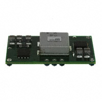
NOMINAL SIZE =
1.5 in x 0.87 in
(38,1 mm x 22,1 mm)
• Up to 22-A Output Current
• 3.3-V Input Voltage
• Wide-Output Voltage Adjust
(0.8 V to 2.5 V)
• Efficiencies up to 93 %
• 120 W/in³ Power Density
• On/Off Inhibit
• Output Voltage Sense
• Pre-Bias Startup
• Margin Up/Down Controls
• Under-Voltage Lockout
• Auto-Track™ Sequencing
• Output Over-Current Protection
(Non-Latching, Auto-Reset)
• Over-Temperature Protection
• Operating Temp: –40 to +85 °C
• IPC Lead Free 2
• Safety Agency Approvals:
UL 1950, CSA 22.2 950, EN60950
VDE (Pending)
• Point-of-load Alliance (POLA)
Compatible
Description
Pin Configuration
The PTH03020 series of non-isolated
power modules offers OEM designers a
combination of high performance, small
footprint, and industry leading features.
As part of a new class of power modules
these products provide designers with the
flexibility to power the most complex
multi-processor digital systems using
off-the-shelf catalog parts.
The series employs double-sided surface
mount construction and provides highperformance step-down power conversion
for up to 22 A of output current from a
3.3-V input bus voltage. The output voltage of the PTH03020W can be set to
any value over the range, 0.8 V to 2.5 V,
using a single resistor.
This series includes Auto-Track™.
Auto-Track simplifies the task of supply
voltage sequencing in a power system by
enabling modules to track each other, or
any external voltage, during power up and
power down.
Other operating features include an
on/off inhibit, output voltage adjust (trim),
and margin up/down controls. To ensure
tight load regulation, an output voltage
sense is also provided. A non-latching
over-current trip and over-tempterature
shutdown provide load fault protection.
Target applications include complex
multi-voltage, multi-processor systems
that incorporate the industry’s high-speed
DSPs, micro-processors and bus drivers.
Pin
1
2
3
4
5
6
7
8
9
10
Function
GND
Vin
Inhibit *
Vo Adjust
Vo Sense
Vout
GND
Track
Margin Down *
Margin Up *
* Denotes negative logic:
Open
= Normal operation
Ground = Function active
™
Track
Auto- n c i n g
e
Sequ
Standard Application
Rset = Required to set the output voltage to a value
higher than 0.8 V. (See spec. table for values)
Cin = Required electrolytic 1,000 µF
Cout = Recommended 330 µF electrolytic
Track
Margin Down
Margin Up
10
9
8
1
7
PTH03020W
(Top View)
V IN
2
V OUT
6
3
4
5
Inhibit
V o Sense
+
GND
For technical support and further information, visit http://power.ti.com
RSET (Required)
0.1 W, 1 %
+
CIN
1,000 µF
(Required)
COUT
330 µF
(Optional)
GND
L
O
A
D
�PTH03020W —3.3-V Input
22-A, 3.3-V Input Non-Isolated
Wide-Output Adjust Power Module
SLTS206C – MAY 2003 – REVISED DECEMBER 2003
Ordering Information
Output Voltage (PTH03020Hxx)
Package Options (PTH03020xHH) (1)
Code
W
Code
AH
AS
Voltage
0.8 V – 2.5 V (Adjust)
Description
Horiz. T/H
SMD, Standard (3)
Pkg Ref.
(EUK)
(EUL)
(2)
Notes: (1) Add “T” to end of part number for tape and reel on SMD packages only.
(2) Reference the applicable package reference drawing for the dimensions and PC board layout
(3) “Standard” option specifies 63/37, Sn/Pb pin solder material.
Pin Descriptions
Vin: The positive input voltage power node to the module, which is referenced to common GND.
Vout: The regulated positive power output with respect
to the GND node.
GND: This is the common ground connection for the
Vin and Vout power connections. It is also the 0 VDC
reference for the control inputs.
Inhibit: The Inhibit pin is an open-collector/drain negative
logic input that is referenced to GND. Applying a lowlevel ground signal to this input disables the module’s
output and turns off the output voltage. When the Inhibit
control is active, the input current drawn by the regulator is significantly reduced. If the Inhibit pin is left
open-circuit, the module will produce an output whenever a valid input source is applied.
Vo Adjust: A 0.1 W, 1 % tolerance (or better) resistor
must be connected between this pin and the GND pin to
set the output voltage to the desired value. The set point
range for the output voltage is from 0.8 V to 2.5 V. The
resistor required for a given output voltage may be calculated from the following formula. If left open circuit,
the module output will default to its lowest output voltage
value. For further information on the adjustment of the
output voltage consult the related application note.
Rset
= 10 k ·
0.8 V
Vout – 0.8 V
– 2.49 k
The specification table gives the preferred resistor values
for a number of standard output voltages.
Vo Sense: The sense input allows the regulation circuit to
compensate for voltage drop between the module and
the load. For optimal voltage accuracy Vo Sense should
be connected to Vout. It can also be left disconnected.
Track: This is an analog control input that enables the
output voltage to follow an external voltage. This pin
becomes active typically 20 ms after the input voltage
has been applied, and allows direct control of the output
voltage from 0 V up to the nominal set-point voltage.
Within this range the output will follow the voltage at
the Track pin on a volt-for-volt basis. When the control
voltage is raised above this range, the module regulates
at its set-point voltage. The feature allows the output
voltage to rise simultaneously with other modules powered from the same input bus. If unused, the input should
be connected to Vin. Note: Due to the under-voltage lockout
feature, the output of the module cannot follow its own input
voltage during power up. For more information, consult the
related application note.
Margin Down: When this input is asserted to GND, the
output voltage is decreased by 5% from the nominal. The
input requires an open-collector (open-drain) interface.
It is not TTL compatible. A lower percent change can
be accomodated with a series resistor. If unused, this
input may be left unconnected. For further information, consult the related application note.
Margin Up: When this input is asserted to GND, the
output voltage is increased by 5%. The input requires an
open-collector (open-drain) interface. It is not TTL
compatible. The percent change can be reduced with a
series resistor. If ununsed, this input may be left unconnected. For further information, consult the related
application note.
For technical support and further information, visit http://power.ti.com
�PTH03020W —3.3-V Input
22-A, 3.3-V Input Non-Isolated
Wide-Output Adjust Power Module
SLTS206C – MAY 2003 – REVISED DECEMBER 2003
Environmental & Absolute Maximum Ratings
Characteristics
Symbols
Track Input Voltage
Operating Temperature Range
Solder Reflow Temperature
Storage Temperature
Mechanical Shock
Vtrack
Ta
Treflow
Ts
Mechanical Vibration
Weight
Flammability
—
—
(Voltages are with respect to GND)
Conditions
Over Vin Range
Surface temperature of module body or pins
—
Per Mil-STD-883D, Method 2002.3
1 msec, ½ Sine, mounted
Mil-STD-883D, Method 2007.2
Suffix H
20-2000 Hz
Suffix S
Min
Typ
–0.3
–40
—
—
Max
Units
Vin + 0.3
85
235 (i)
125
V
°C
°C
°C
–40
—
—
500
—
G’s
—
—
—
20
10
5
—
—
—
G’s
grams
Meets UL 94V-O
Notes: (i) During reflow of SMD package version do not elevate peak temperature of the module, pins or internal components above the stated maximum.
Specifications
(Unless otherwise stated, T a =25 °C, V in =3.3 V, Vout =2 V, Cin =1,000 µF, Cout =0 µF, and I o =Iomax)
Characteristics
Symbols
Conditions
Min
Output Current
Io
Input Voltage Range
Set-Point Voltage Tolerance
Temperature Variation
Line Regulation
Load Regulation
Total Output Variation
Vin
Vo tol
∆Regtemp
∆Regline
∆Regload
∆Regtot
60 °C, 200 LFM airflow
25 °C, natural convection
Over Io range
0
0
2.95 (2)
—
—
—
—
Efficiency
η
Vo Ripple (pk-pk)
Over-Current Threshold
Transient Response
Vr
Io trip
Margin Up/Down Adjust
Margin Input Current (pins 9 /10)
Track Input Current (pin 8)
Track Slew Rate Capability
Under-Voltage Lockout
ttr
∆Vtr
Vo adj
IIL margin
IIL track
dVtrack/dt
UVLO
Inhibit Control (pin3)
Input High Voltage
Input Low Voltage
Input Low Current
VIH
VIL
IIL inhibit
Input Standby Current
Switching Frequency
External Input Capacitance
External Output Capacitance
Iin inh
ƒs
Cin
Cout
Reliability
MTBF
–40 °C


 工商网监
湘ICP备2023018690号
工商网监
湘ICP备2023018690号

