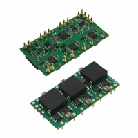
PTH04040W
www.ti.com
SLTS238C – SEPTEMBER 2005 – REVISED JUNE 2010
60-A, 3.3/5-V INPUT, NONISOLATED WIDE-OUTPUT
ADJUST POWER MODULE
Check for Samples: PTH04040W
FEATURES
APPLICATIONS
•
•
•
•
•
•
•
•
1
2
•
•
•
•
•
•
•
•
60-A Output Current
3.3-V and 5-V Input Voltage
Wide-Output Voltage Adjust (0.8 V to 2.5 V)
Efficiencies up to 93%
On/Off Inhibit
Differential Output Sense
Output Overcurrent Protection
(Nonlatching, Auto-Reset)
Overtemperature Protection
Auto-Track™ Sequencing
Start Up Into Output Prebias
Margin Up/Down Controls
Operating Temperature: –40°C to 85°C
Multi-Phase, Switch-Mode Topology
Programmable Undervoltage Lockout (UVLO)
Safety Agency Approvals:
UL/IEC/CSA-22.2 60950-1
Advanced Computing and Server Applications
NOMINAL SIZE =
2.05 in x 1.05 in
(52 mm x 26,7 mm)
DESCRIPTION
The PTH04040W is a high-performance 60-A rated, nonisolated, power module, which uses the latest
multi-phase switched-mode topology. This provides a small, ready-to-use module, that can power the most
densely populated multiprocessor systems.
The PTH04040W operates over an input voltage range of 2.95 V to 5.5 V, and can be set to any output voltage
over the range, 0.8 V to 2.5 V, using a single external resistor. The combination of a wide input voltage and
wide-output adjust range allows the PTH04040W to be used in many of high-performance applications. These
include advanced computing platforms and servers that utilize either a 3.3-V or 5-V distribution bus.
These modules incorporate a comprehensive list of features. They include an on/off inhibit and margin up/down
controls. A differential remote output voltage sense ensures tight load regulation, and an output overcurrent and
overtemperature shutdown protect against most load faults. A programmable undervoltage lockout allows the
turn-on threshold to be customized.
The PTH04040W incorporates Auto-Track™. Auto-Track is a popular feature of the PTH family that allows the
outputs of multiple modules to track a common voltage during power-up and power-down transitions. This greatly
simplifies the sequencing of voltages for VLSI ICs that operate off multiple power rails.
The double-sided surface mount construction has a low profile and compact footprint. It is available in both
throughhole and surface-mount packages.
1
2
Please be aware that an important notice concerning availability, standard warranty, and use in critical applications of Texas
Instruments semiconductor products and disclaimers thereto appears at the end of this data sheet.
Auto-Track, POLA, TMS320 are trademarks of Texas Instruments.
PRODUCTION DATA information is current as of publication date.
Products conform to specifications per the terms of the Texas
Instruments standard warranty. Production processing does not
necessarily include testing of all parameters.
Copyright © 2005–2010, Texas Instruments Incorporated
�PTH04040W
SLTS238C – SEPTEMBER 2005 – REVISED JUNE 2010
www.ti.com
This integrated circuit can be damaged by ESD. Texas Instruments recommends that all integrated circuits be handled with
appropriate precautions. Failure to observe proper handling and installation procedures can cause damage.
ESD damage can range from subtle performance degradation to complete device failure. Precision integrated circuits may be more
susceptible to damage because very small parametric changes could cause the device not to meet its published specifications.
STANDARD APPLICATION
19
Margin
Up
2
VI
4
20
Margin
Down
8
+Sense
11
9
PTH04040W
Vo
12
VO
15
UVLO
Inhibit
A
Track
VI
6
+
18
CI
1000 µF
(Required)
7
GND
1
3
GND
5
10
13
−Sense
VoAdj
14
+
16 17
RSET B
1%
0.05 W
C
+
CO1
330 µF
C
CO2
330 µF
UDG−05085
A.
For CI, a minimum of 1,000 mF (or 2 × 470 mF) of input capacitance is required for proper operation.
B.
RSET is required to set the desired output voltage from the module higher than the minimum value.
C.
For CO1 and CO2, a minimum of 660 mF (or 2 × 330 mF) of output capacitance is required for load transient
regulation.
ORDERING INFORMATION
For the most current package and ordering information, see the Package Option Addendum at the end of this datasheet, or see
the TI website at www.ti.com.
ABSOLUTE MAXIMUM RATINGS
over operating free-air temperature range (unless otherwise noted)
UNIT
Signal input voltages
Track control (pin 18)
TA
Operating temperature range over VI range
Twave
Wave solder
temperature
Surface temperature of module body or pins
(5 seconds)
Treflow
Solder reflow
temperature
Surface temperature of module body or pins
TS
Storage temperature
–40°C to 85°C
2
260°C
(1)
PTH04040WAS
235°C
(1)
PTH04040WAZ
260°C
(1)
–55°C to 125°C
Per Mil-STD-883D, Method 2002.3, 1 msec, ½ Sine, mounted
500 G (2)
Mechanical vibration
Mil-STD-883D, Method 2007.2, 20–2000 Hz
10 G (2)
Flammability
(2)
PTH04040WAH
PTH04040WAD
Mechanical shock
Weight
(1)
–0.3 V to VI + 0.3 V
22.5 grams
Meets UL94V-O
During soldering of package version, do not elevate peak temperature of the module, pins or internal components above the stated
maximum.
Qualification limits
Submit Documentation Feedback
Copyright © 2005–2010, Texas Instruments Incorporated
Product Folder Link(s): PTH04040W
�PTH04040W
www.ti.com
SLTS238C – SEPTEMBER 2005 – REVISED JUNE 2010
ELECTRICAL CHARACTERISTICS
TA = 25°C, VI = 5 V, VO = 2.5 V, CI = 1000 µF, CO = 660 µF, and IO = IOmax (unless otherwise stated)
PARAMETER
TEST CONDITIONS
MIN
MAX
UNIT
0
TYP
60 (1)
A
2.95 (2)
5.5
IO
Output current
60°C, 200 LFM airflow
VI
Input voltage range
Over IO range
VOtol
Set-point voltage tolerance
ΔRegtemp
Temperature variation
–40°C < TA < 85°C
±0.5
%VO
ΔRegline
Line regulation
Over VI range
±5
mV
ΔRegload
Load regulation
Over IO range
±5
ΔRegtot
Total output variation
Includes set-point, line, load, –40°C ≤ TA ≤ 85°C
VO,
Output adjust range
ADJ
±2 (3)
VI = 5 V, IO = 45 A
Efficiency
h
VI = 3.3 V, IO = 45 A
mV
±3 (3)
2.95 ≤ VI ≤ 4.5 V (3)
0.8
-
1.65
4.5 < VI ≤ 5.5 V (3)
0.8
-
2.5
RSET = 2.21 kΩ, VO = 2.5 V
93%
RSET = 5.49 kΩ, VO = 1.8 V
90%
RSET = 8.87 kΩ, VO = 1.5 V
88%
RSET = 17.4 kΩ, VO = 1.2 V
86%
RSET = 6.92 kΩ, VO = 1.65 V
92%
RSET = 8.87 kΩ, VO = 1.5 V
91%
RSET = 36.5 kΩ, VO = 1 V
87%
All voltages
15
V
%VO
%VO
V
VR
VO ripple (peak-to-peak)
20-MHz bandwidth
IOtrip
Overcurrent threshold
Reset, followed by auto-recovery
Transient response
1 A/µs load step, 50 to 100%
IOmax, CO=660µF
Margin up down adjust
From a given set-point voltage
±5%
%
IILmargin
Margin input current
Pin to GND
–8 (4)
µA
IILtrack
Track input current (pin 18)
Pin to GND
dV/dt
Track slew rate capability
|VTRACK – VO | ≤ 50 mV and V(TRACK) < VO(nom)
UVLO
Undervoltage lockout
Pin 8 open
trr
ΔVtr
Inhibit control (pin 7)
Recovery time
VO over/undershoot
mVPP
90
A
100
µS
200
mV
–0.11 (5)
1
On-threshold
2.6 (6)
Hysterisis
0.6 (6)
mA
V/ms
V
Input high voltage (VIH), Referenced to GND
2.5
Open (7)
Input low voltage (VIL), Referenced to GND
–0.2
0.5
V
Input low current (IIL), Pin to GND
0.5
mA
IIinh
Input standby current
Inhibit (pin 7) to GND
60
mA
fs
Switching frequency
Over VI and IO ranges
(1)
(2)
(3)
(4)
(5)
(6)
(7)
675
825
975
kHz
See SOA curves or consult factory for appropriate derating.
The nominal input voltage must be at least 2 × VO. Output voltage regulation is specified with an input voltage within ±10% from nominal
3.3 V or 5 V. For example, for VI = 5 V and VO = 2.5 V, the input can vary between 4.5 V and 5.5 V.
The set-point voltage tolerance is affected by the tolerance of RSET. The stated limit is unconditionally met if RSET has a tolerance of 1%
with 100 ppm/°C or better temperature stability.
A small, low-leakage (4500 mA
>5440 mA
10x10.5
10x12.7
2 (2)
2
≤5
≤4
10SP470M
6SVP820M
Panasonic, Poly-Aluminum:
S/SE (SMD)
63 V
180
0.005 Ω
4000 mA
7.3x4.3x4.2
N/R
≤2
EEFSE0J181R
10 V
10 V
470
470
0.045 Ω
0.060 Ω
1723 mA
1826 mA
7.3x5.7x4.1
7.3x5.7x4.1
2 (2)
2 (2)
≤7
≤7
TPSE477M010R0045
TPSV477M010R0060
6.3 V
10 V
6.3 V
470
330
470
0.018 Ω
0.015 Ω
0.012 Ω
>1200 mA
>3800 mA
4200 mA
7.3x4.3x4
7.3x4.3x4
7.3x4.3x4
2 (2)
3
2 (2)
≤6
≤4
≤3
T520X477M006SE018
T530X337M010AS
T530X477M006AS
595D, Tantalum (SMD)
94SA, Os-con (Radial)
10 V
16 V
470
2200
0.100 Ω
0.015 Ω
1440 mA
9740 mA
7.2x6×4.1
16 × 25
2 (2)
1
≤7
≤4
595D477X0010R2T
94SA108X0016HBP
Kemet, Ceramic X5R (SMD)
16 V
6.3 V
10
47
0.002 Ω
0.002 Ω
–
1210 case
3225 mm
1 (3)
1 (3)
≤9
≤8
C1210C106M4PAC
C1210C476K9PAC
Murata, Ceramic X5R (SMD)
6.3 V
6.3 V
16 V
16 V
100
47
22
10
0.002 Ω
–
1210 case
3225 mm
1 (3)
1 (3)
1 (3)
≤4
≤8
≤8
≤9
GRM32ER60J107M
GRM32ER60J476M
GRM32ER61C226K
GRM32DR61C106K
TDK, Ceramic X5R (SMD)
6.3 V
6.3 V
16 V
16 V
100
47
22
10
0.002 Ω
–
1210 case
3225 mm
1 (3)
1 (3)
1 (3)
≤4
≤8
≤8
≤9
C3225X5R0J107MT
C3225X5R0J476MT
C3225X5R1C226MT
C3225X5R1C106MT
Physical
Size (mm)
Input
Bus
Output
Bus
Vendor Part No.
Panasonic
FC (Radial)
FC (Radial)
FK (SMD)
United Chemi-Con
FX, Oscon (Radial)
PXA, (Poly-Aluminum (SMD)
PSA (Poly-Aluminum)
LXZ, Aluminum (Radial)
Nichicon, Aluminum
HD (Radial)
PM (Radial)
Sanyo, Os-Con
AVX, Tantalum, Series III
TPS (SMD)
Kemet, Poly-Tantalum
T520 (SMD)
T530 (SMD)
Vishay-Sprague
(1)
(2)
(3)
10
Capacitor Supplier Verification
1.Please verify availability of capacitors identified in this table. Capacitor suppliers may recommend alternative part numbers because of
limited availability or obsolete products. In some instances, the capacitor product life cycle may be in decline and have short-term
consideration for obsolescence.
RoHS, Lead-free and Material Details
2.Please consult capacitor suppliers regarding material composition, RoHS status, lead-free status, and manufacturing process
requirements. Component designators or part number deviations can occur when material composition or soldering requirements are
updated.
The total capacitance is slightly lower than 1000 mF, but is acceptable based on the combined ripple current rating.
Ceramic capacitors can be used to complement electrolytic types at the input to further reduce high-frequency ripple current.
Submit Documentation Feedback
Copyright © 2005–2010, Texas Instruments Incorporated
Product Folder Link(s): PTH04040W
�PTH04040W
www.ti.com
SLTS238C – SEPTEMBER 2005 – REVISED JUNE 2010
ADJUSTING THE OUTPUT VOLTAGE OF THE PTH04040W
The VO Adjust control (pin 17) sets the output voltage of the PTH04040W to a value higher than 0.8 V. The
adjustment range is from 0.8 V to 2.5 V. For an output voltage other than 0.8 V a single external resistor, RSET 1,
must be connected directly between the VO Adjust (pin 17) and the output GND (pin 16)(2). Table 2 gives the
preferred value of the external resistor for a number of standard voltages, along with the actual output voltage
that this resistance value provides.
For other output voltages, the value of the required resistor is calculated using the following formula, or by
selecting from the range of values given in Table 3. Figure 9 shows the placement of the required resistor.
0.8 V
R set + 10 kW
* 2.49 kW
V out * 0.8 V
(1)
Table 2. Preferred Values of Rset for Standard Output Voltages
VOUT (Standard)
(1)
(1)
RSET (Preferred Value)
VOUT (Actual)
2.5 V
2.21 kΩ
2.502 V
2V
4.12 kΩ
2.010 V
1.8 V
5.49 kΩ
1.803 V
1.5 V
8.87 kΩ
1.504 V
1.2 V
17.4 kΩ
1.202 V
1V
36.5 kΩ
1.005 V
0.8 V
Open
0.8 V
The nominal input voltage must be at least 2 × VO. Output voltage regulation is specified with an input voltage within ±10% from nominal
3.3 V or 5 V. For example, for VI = 5 V and VO = 2.5 V, the input can vary between 4.5 V and 5.5 V.
18
Track
+Sense 11
9
VO
PTH04040W
VO
12
15
−Sense 14
GND
10 13
Adjust
16
17
RSET
1%
0.05 W
CO
GND
GND
Figure 9. VO Adjust Resistor Placement
Submit Documentation Feedback
Copyright © 2005–2010, Texas Instruments Incorporated
Product Folder Link(s): PTH04040W
11
�PTH04040W
SLTS238C – SEPTEMBER 2005 – REVISED JUNE 2010
www.ti.com
Table 3. Output Voltage Set-Point Resistor Values
VOUT
RSET
VOUT
RSET
0.8
Open
1.425
10.3 kΩ
0.825
318 kΩ
1.45
9.82 kΩ
0.85
158 kΩ
1.475
9.36 kΩ
0.875
104 kΩ
1.5
8.94 kΩ
0.9
77.5 kΩ
1.55
8.18 kΩ
0.925
61.5 kΩ
1.6
7.51 kΩ
0.95
50.8 kΩ
1.65
6.92 kΩ
0.975
43.2 kΩ
1.7
6.4 kΩ
1
37.5 kΩ
1.75
5.93 kΩ
1.025
33.1 kΩ
1.8
5.51 kΩ
1.05
29.5 kΩ
1.85
5.13 kΩ
1.075
26.6 kΩ
1.9
4.78 kΩ
1.1
24.2 kΩ
1.95
4.47 kΩ
1.125
22.1 kΩ
2
4.18 kΩ
1.15
20.4 kΩ
2.05
3.91kΩ
1.175
18.8 kΩ
2.1
3.66 kΩ
1.2
17.5 kΩ
2.15
3.44 kΩ
1.225
16.3 kΩ
2.2
3.22 kΩ
1.25
15.3 kΩ
2.25
3.03 kΩ
1.275
14.4 kΩ
2.3
2.84 kΩ
1.3
13.5 kΩ
2.35
2.67 kΩ
1.325
12.7 kΩ
2.4
2.51 kΩ
1.35
12.1 kΩ
2.45
2.36 kΩ
1.375
11.4 kΩ
2.5
2.22 kΩ
1.4
10.8 kΩ
NOTES:
1. A 0.05-W rated resistor can be used. The tolerance should be 1%, with temperature stability of 100 ppm/°C
(or better). Place the resistor as close to the regulator as possible. Connect the resistor directly between pins
17 and 16 using dedicated PCB traces.
2. Never connect capacitors from VO Adjust to either GND or VO . Any capacitance added to the VO Adjust pin
affects the stability of the regulator.
12
Submit Documentation Feedback
Copyright © 2005–2010, Texas Instruments Incorporated
Product Folder Link(s): PTH04040W
�PTH04040W
www.ti.com
SLTS238C – SEPTEMBER 2005 – REVISED JUNE 2010
ADJUSTING THE UNDERVOLTAGE LOCKOUT (UVLO) OF THE PTH04040W
The PTH04040W power modules incorporate an input undervoltage lockout (UVLO). The UVLO feature prevents
the operation of the module until there is sufficient input voltage to produce a valid output voltage. This enables
the module to provide a monotonic powerup for the load circuit, and also limits the magnitude of current drawn
from the module’s input source during the power-up sequence.
The UVLO characteristic is defined by the on-threshold (VTHD) and hysterisis (VHYS) voltages. Below the on
threshold, the Inhibit control is overriden, and the module does not produce an output. Hysterisis voltage is the
difference between the on and off threshold voltages. It ensures a clean power-up, even when the input voltage
is rising slowly. The hysterisis prevents start-up oscillations, which can occur if the input voltage droops slightly
when the module begins drawing current from the input source.
UVLO ADJUSTMENT
The UVLO feature of the PTH04040W gives the user the option of adjusting the on-threshold voltage higher than
the default value. This might be desirable if the module is powered from a 5-V input bus. This prevents the
module from operating until the input bus has risen closer to its regulation voltage.
The adjustment method uses the UVLO Prog control (pin 8). If the UVLO Prog pin is left open circuit, the
onthreshold voltage remains at its nominal value of 2.63 V (see electrical specification table). This ensures that
the unadjusted module produces a regulated output when the minimum input voltage is applied. The hysterisis
voltage is approximately 0.62 V, which correlates to an off-threshold voltage of about 2 V. The magnitude of the
hysterisis is automatically set to about 22% of the onthreshold. So if the on-threshold voltage is increased, then
the Hysterisis also increases.
UVLO ADJUSTMENT METHOD
Figure 10 shows the placement of the resistor, RTHD, for adjusting the UVLO on-threshold voltage. It connects
from the UVLO Prog control pin to GND. Equation 2 determines the value of RTHD required to adjust VTHD to a
new value. The default value is 2.63 V, and it can only be adjusted higher. Once the value of RTHD has been set,
Equation 3 is used to determine the new hysterisis voltage.
R THD
12.9
=
kΩ
VTHD − 2.63
VHYS = 2.191
1
R THD
(2)
+ 0.283
V
(3)
2
VI
4
6
8
VI
PTH04040W
UVLO Prog
Inhibit
7
CI
GND
1
3 5
RTHD
1,000 mF
GND
Figure 10. UVLO Program Resistor Placement
Submit Documentation Feedback
Copyright © 2005–2010, Texas Instruments Incorporated
Product Folder Link(s): PTH04040W
13
�PTH04040W
SLTS238C – SEPTEMBER 2005 – REVISED JUNE 2010
www.ti.com
FEATURES OF THE PTH FAMILY OF NONISOLATED WIDE OUTPUT ADJUST POWER
MODULES
POLA™ COMPATIBILITY
The PTH/PTV family of nonisolated, wide-output adjustable power modules are optimized for applications that
require a flexible, high performance module that is small in size. Each of these products are POLA™ compatible.
POLA-compatible products are produced by a number of manufacturers, and offer customers advanced,
nonisolated modules with the same footprint and form factor. POLA parts are also assured to be interoperable,
thereby providing customers with second-source availability.
Many of the POLA-compatible parts include a feature called Auto-Track™. Auto-Track was specifically designed
to simplify the task of sequencing the supply voltages in a power system. This and other features are described
the following sections.
SOFT-START POWER UP
The Auto-Track feature allows the power-up of multiple PTH modules to be directly controlled from the Track pin.
However in a stand-alone configuration, or when the Auto-Track feature is not being used, the Track pin should
be directly connected to the input voltage, Vin (see Figure 11).
5V
2
VI
Dn
8
5
Track
Sense
VO
PTH05020W
Inhibit
3
3.3 V
6
VO (1 V/Div)
Adjust
GND
1
VI (1 V/Div)
7
4
CI
RSET
1,000 mF
698 W
0.1 W, 1%
+
GND
+
10 9
Up
II (5 A/Div)
CO
330 mF
GND
Figure 11. Power-Up Application Circuit
t - Time = 5 msec/Div
Figure 12. Power-Up Waveforms
When the Track pin is connected to the input voltage the Auto-Track function is permanently disengaged. This
allows the module to power up entirely under the control of its internal soft-start circuitry. When power up is
under soft-start control, the output voltage rises to the set-point at a quicker and more linear rate.
From the moment a valid input voltage is applied, the soft-start control introduces a short time delay (typically
5 ms–10 ms) before allowing the output voltage to rise. The output then progressively rises to the module’s
setpoint voltage. Figure 12 shows the soft-start power-up characteristic of the 22-A output product
(PTH05020W), operating from a 5-V input bus and configured for a 3.3-V output. The waveforms were measured
with a 5-A resistive load and the Auto-Track feature disabled. The initial rise in input current when the input
voltage first starts to rise is the charge current drawn by the input capacitors. Power-up is complete within 15 ms.
14
Submit Documentation Feedback
Copyright © 2005–2010, Texas Instruments Incorporated
Product Folder Link(s): PTH04040W
�PTH04040W
www.ti.com
SLTS238C – SEPTEMBER 2005 – REVISED JUNE 2010
OVERCURRENT PROTECTION
For protection against load faults, all modules incorporate output overcurrent protection. Applying a load that
exceeds the regulator’s overcurrent threshold causes the regulated output to shut down. Following shutdown, a
module periodically attempts to recover by initiating a soft-start powerup. This is described as a hiccup mode of
operation, whereby the module continues in a cycle of successive shutdown and power up until the load fault is
removed. During this period, the average current flowing into the fault is significantly reduced. Once the fault is
removed, the module automatically recovers and returns to normal operation.
OVERTEMPERATURE PROTECTION (OTP)
Products with a high output current capability (>20 A), incorporate overtemperature protection. This feature is
provided by an on-board temperature sensor that protects the module’s internal circuitry against excessively high
temperatures. A rise in the internal temperature may be the result of a drop in airflow, or a high ambient
temperature. If the internal temperature exceeds the OTP threshold, the module’s Inhibit control is automatically
pulled low. This turns the output off. The output voltage drops as the external output capacitors are discharged
by the load circuit. The recovery is automatic, and begins with a soft-start power up. It occurs when the sensed
temperature decreases by about 10°C below the trip point.
Note: The overtemperature protection is a last resort mechanism to prevent thermal stress to the regulator.
Operation at or close to the thermal shutdown temperature is not recommended, and reduces the long-term
reliability of the module. Always operate the regulator within the specified safe operating area (SOA) limits for
the worst-case conditions of ambient temperature and airflow.
OUTPUT ON/OFF INHIBIT
For applications requiring output voltage on/off control, each series of the PTH family incorporates an output
Inhibit control pin. The inhibit feature can be used wherever there is a requirement for the output voltage from the
regulator to be turned off.
The power modules function normally when the Inhibit pin is left open-circuit, providing a regulated output
whenever a valid source voltage is connected to Vin with respect to GND.
Figure 13 shows the typical application of the inhibit function. Note the discrete transistor (Q1). The Inhibit control
has its own internal pull-up to VI potential. The input is not compatible with TTL logic devices. An open-collector
(or open-drain) discrete transistor is recommended for control.
VOSense
VO (2 V/Div)
VI
2
1,000 mF
1 = Inhibit
5
8
6
PTH05020W
3
+
CI
9
1
4
7
RSET
Q1
BSS138
CO
VO
330 mF
GND
II (2 A/Div)
L
O
A
D
+
10
Q1Vds (5 V/Div)
GND
Figure 13. Inhibit Control Circuit
t - Time = 10 msec/Div
Figure 14. Power-Up from Inhibit Control
Turning Q1 on applies a low voltage to the Inhibit control and disables the output of the module. If Q1 is then
turned off, the module executes a soft-start powerup. A regulated output voltage is produced within 20 ms.
Figure 14 shows the typical rise in both the output voltage and input current, following the turn-off of Q1. The turn
off of Q1 corresponds to the rise in the waveform, Q1 Vds. The waveforms were measured with a 5-A constant
current load.
Submit Documentation Feedback
Copyright © 2005–2010, Texas Instruments Incorporated
Product Folder Link(s): PTH04040W
15
�PTH04040W
SLTS238C – SEPTEMBER 2005 – REVISED JUNE 2010
www.ti.com
REMOTE SENSE
The remote sense feature allows the regulator to compensate for limited amounts of voltage drop, that may be
incurred between the converter and load, due to resistance in the PCB traces. Connecting the +Sense and
–Sense pins to the respective VO and GND output nodes improves the load regulation of the regulator output at
those connection points. This is recommended even if the load circuit is located close to the module.
If either the +Sense and –Sense are left open-circuit, an internal low-value resistor (15-Ω or less), connected
from the respective sense pin to either VO or GND, ensures the output voltage remains in regulation.
With the sense pins connected, the difference between the voltage measured across the VO and GND pins of the
regulator, and that measured at +Sense with respect to +Sense, is the amount of IR drop being compensated by
the regulator. This should be limited to a maximum of 0.3 V.
Note: The remote sense feature is not designed to compensate for the forward drop of nonlinear or
frequency dependent components that may be placed in series with the converter output. Examples include
OR-ing diodes, filter inductors, ferrite beads, and fuses. When these components are enclosed by the remote
sense connection they are effectively placed inside the regulation control loop, which can adversely affect the
stability of the regulator.
Auto-Track™ FUNCTION
The Auto-Track function is unique to the PTH/PTV family, and is available with the all POLA-compatible
products. Auto-Track was designed to simplify the amount of circuitry required to make the output voltage from
each module power up and power down in sequence. The sequencing of two or more supply voltages during
power up is a common requirement for complex mixed-signal applications, that use dual-voltage VLSI ICs such
as the TMS320™ DSP family, micro-processors, and ASICs.
HOW Auto-Track WORKS
Auto-Track works by forcing the module’s output voltage to follow a voltage presented at the Track control pin.
This control range is limited to between 0 V and the module’s set-point voltage. Once the Track input is raised
above the set-point voltage, the module’s output remains at its set-point 1. As an example, if the Track pin of a
2.5-V regulator is at 1 V, the regulated output will be 1 V. But, if the voltage at the Track pin rises to 3 V, the
regulated output does not go higher than 2.5 V.
When the Track input is used to connect a number of modules together, it forces the output voltage from each
module to follow a common signal during power-up and power-down. The control signal can be an externally
generated master ramp waveform, or the output voltage from another power supply circuit.(3) For convenience,
each module’s Track input incorporates an internal RC charge circuit. This operates off the module’s input
voltage to provide a suitable rising voltage ramp waveform.
TYPICAL Auto-Track APPLICATION
Connecting the Track inputs of two or more modules forces their Track input to follow the same collective RC
ramp waveform, and allows their power-up sequence to be coordinated from a common Track control signal.
This can be an open-collector (or open drain) device, such as a power-up reset voltage supervisor IC.
To coordinate a power-up sequence the Track control must first pulled to ground potential. This should be done
at or before input power is applied to the modules. The ground signal should be maintained for at least 10 ms
after input power has been applied. This brief period gives the modules time to complete their internal soft-start
initialization, enabling them to produce an output voltage. A low-cost supply voltage supervisor IC, that includes
built-in time delay, is an ideal component for automatically controlling the Track inputs at power up.
Figure 17 shows how the TPS3808G50 supply voltage supervisor IC (U3) can be used to coordinate the
sequenced power-up of two 5-V input Auto-Track modules. The output of the TPS3808 supervisor becomes
active above an input voltage of 0.8 V, enabling it to assert a ground signal to the common Track control well
before the input voltage has reached the module’s undervoltage lockout threshold. The ground signal is
maintained until approximately 27 ms after the input voltage has risen above U3’s voltage threshold, which is
4.65 V. The 27-ms time period is controlled by the capacitor C3. The value of 4700 mF provides sufficient time
delay for the modules to complete their internal soft-start initialization. The output voltage of each module
remains at zero until the Track control voltage is allowed to rise. When U3 removes the ground signal, the Track
control voltage automatically rises to the input voltage. This causes the output voltage of each module to rise
simultaneously with the other modules, until each reaches its respective set-point voltage.
16
Submit Documentation Feedback
Copyright © 2005–2010, Texas Instruments Incorporated
Product Folder Link(s): PTH04040W
�PTH04040W
www.ti.com
SLTS238C – SEPTEMBER 2005 – REVISED JUNE 2010
Figure 15 shows the output voltage waveforms from the circuit of Figure 17 after input voltage is applied to the
circuit. The waveforms, VO1 and VO2, represent the output voltages from the two power modules, U1 (3.3 V) and
U2 (1.8 V), respectively. VTRK, VO1, and VO2 are shown rising together to produce the desired simultaneous
power-up characteristic.
The same circuit also provides a power-down sequence. When the input voltage falls below U3's voltage
threshold, the ground signal is re-applied to the common Track control. This pulls the Track inputs to zero volts,
forcing the output of each module to follow, as shown in Figure 16. In order for a simultaneous power-down to
occur, the Track inputs must be pulled low before the input voltage has fallen below the modules' undervoltage
lockout. This is an important constraint. Once the modules recognize that a valid input voltage is no longer
present, their outputs can no longer follow the voltage applied at their Track input. During a power-down
sequence, the fall in the output voltage from the modules is limited by the maximum output capacitance and the
Auto-Track slew rate.
NOTES ON USE OF Auto-Track
1. The Track pin voltage must be allowed to rise above the module’s set-point voltage before the module can
regulate at its adjusted set-point voltage.
2. The Auto-Track function tracks almost any voltage ramp during power up, and is compatible with ramp
speeds of up to 1 V/ms.
3. The absolute maximum voltage that may be applied to the Track pin is VI.
4. The module does not follow a voltage at its Track input until it has completed its soft-start initialization. This
takes at least 10 ms from the time that the module has sensed that a valid voltage is present. During this
period, the Track input should be held at ground potential.
5. The module is capable of both sinking and sourcing current when following a voltage at its Track input.
Therefore startup into an output prebias is not supported when the module is under Auto-Track control.
Prebias hold off is not necessary when all supply voltages simultaneously under the control of Auto-Track.
6. The Auto-Track function can be disabled by connecting the Track pin to the input voltage (VI). With
Auto-Track disabled, the output voltage rises at a quicker and more linear rate after input power is applied.
VTRK (1 V/div)
VTRK (1 V/div)
V01 (1 V/div)
V01 (1 V/div)
V02 (1 V/div)
V02 (1 V/div)
t − Time − 20 ms/div
t − Time − 200 µs/div
Figure 15. Auto-Track Simultaneous Power Up
Waveforms
Figure 16. Auto-Track Simultaneous Power Down
Waveforms
Submit Documentation Feedback
Copyright © 2005–2010, Texas Instruments Incorporated
Product Folder Link(s): PTH04040W
17
�PTH04040W
SLTS238C – SEPTEMBER 2005 – REVISED JUNE 2010
www.ti.com
14
U1
13
Track
TT
+Sense
+5 V
2, 6
VI
VO
PTH05T210W
10
5, 9
VO1 = 3.3 V
1
−Sense
INH/UVLO
11
VOAdj
GND GND
3, 4
7, 8
+
12
CO1
+
CI1
RSET1
1.62 kΩ
U3
6
VCC
5
3
MR SENSE
C4
0.1 µF
RESET
4 TPS3808G50
CT
GND
C3
4700 pF
1
RTRK#
50 Ω
U2
2
19
20
18
Margin Margin Track
Up Down
+Sense
VI
2
4
6
8
RTRK# = 100 Ω/N
N = Number of track pins connected together
11
9
VI
VO
PTH04040W
−Sense
UVLO Prog
Inhibit
7
GND
1
3
GND
5
12
15
VOAdj
10 13 16
VO2 = 1.8 V
14
17
+
+
CO2
CI2
RSET2
5.49 kΩ
Figure 17. Sequenced Power Up and Power Down using Auto-Track
18
Submit Documentation Feedback
Copyright © 2005–2010, Texas Instruments Incorporated
Product Folder Link(s): PTH04040W
�PTH04040W
www.ti.com
SLTS238C – SEPTEMBER 2005 – REVISED JUNE 2010
MARGIN UP/DOWN CONTROLS
The PTHxx060, PTHxx010, PTHxx020, and PTHxx030 products incorporate Margin Up and Margin Down control
inputs. These controls allow the output voltage to be momentarily adjusted(1), either up or down, by a nominal
5%. This provides a convenient method for dynamically testing the operation of the load circuit over its supply
margin or range. It can also be used to verify the function of supply voltage supervisors. The ±5% change is
applied to the adjusted output voltage, as set by the external resistor, Rset at the Vo Adjust pin.
The 5% adjustment is made by pulling the appropriate margin control input directly to the GND terminal 2. A
low-leakage open-drain device, such as an n-channel MOSFET or p-channel JFET is recommended for this
purpose(3). Adjustments of less than 5% can also be accommodated by adding series resistors to the control
inputs. The value of the resistor can be selected from Table 4, or calculated using the following formula.
UP/DOWN ADJUST RESISTANCE CALCULATION
RU or RD =
499
- 99.8 kW
D%
(4)
Where Δ% = The desired amount of margin adjusted in percent.
NOTES
1. The Margin Up and Margin Down controls were not intended to be activated simultaneously. If they are
activated simultaneously, the effects on the output voltage may not completely cancel, resulting in the
possibility of a higher error in the output voltage set point.
2. The ground reference should be a direct connection to the module GND at pin 7 (pin 1 for the PTHxx050).
This produces a more accurate adjustment at the load circuit terminals. The transistors Q1 and Q2 should be
located close to the regulator.
3. The Margin Up and Margin Down control inputs are not compatible with devices that source voltage. This
includes TTL logic. These are analog inputs and should only be controlled with a true open-drain device
(preferably discrete MOSFET transistor). The device selected should have low off-state leakage current.
Each input sources 8 µA when grounded, and has an open-circuit voltage of 0.8 V.
Table 4. Margin Up/Down Resistor Values
% ADJUST
5%
4%
3%
2%
1%
RU / RD
0 kΩ
24.9 kΩ
66.5 kΩ
150.0 kΩ
397.0 kΩ
1
9
10
8
7
+VO
0V
PTH05010W
(Top View)
VI
2
3
CI
+
RD
RU
+VO
6
4
5
RSET
0.1 W, 1%
+
CO
L
O
A
D
Q1
Margin Down
Q2
Margin Up
GND
GND
Figure 18. Margin Up/Down Application Schematic
Submit Documentation Feedback
Copyright © 2005–2010, Texas Instruments Incorporated
Product Folder Link(s): PTH04040W
19
�PTH04040W
SLTS238C – SEPTEMBER 2005 – REVISED JUNE 2010
www.ti.com
PREBIAS STARTUP CAPABILITY
A prebias startup condition occurs as a result of an external voltage being present at the output of a power
module prior to its output becoming active. This often occurs in complex digital systems when current from
another power source is backfed through a dual-supply logic component, such as an FPGA or ASIC. Another
path might be via clamp diodes as part of a dual-supply power-up sequencing arrangement. A prebias can cause
problems with power modules that incorporate synchronous rectifiers. This is because under most operating
conditions, these types of modules can sink as well as source output current.
The PTH/PTV family of power modules incorporate synchronous rectifiers, but does not sink current during
startup(1), or whenever the Inhibit pin is held low. However, to ensure satisfactory operation of this function,
certain conditions must be maintained(2). Figure 19 shows an application demonstrating the prebias startup
capability. The start-up waveforms are shown in Figure 20. Note that the output current from the PTH03010W (Io)
shows negligible current until its output voltage rises above that backfed through diodes D1 and D2.
Note: The prebias start-up feature is not compatible with Auto-Track. When the module is under Auto-Track
control, it sinks current if the output voltage is below that of a back-feeding source. To ensure a prebias
hold-off, one of two approaches must be followed when input power is applied to the module. The Auto-Track
function must be disabled(3), or the module’s output held off (for at least 50 ms) using the Inhibit pin. Either
approach ensures that the Track pin voltage is above the set-point voltage at start up.
NOTES
1. Startup includes the short delay (approximately 10 ms) prior to the output voltage rising, followed by the rise
of the output voltage under the module’s internal soft-start control. Startup is complete when the output
voltage has risen to either the set-point voltage or the voltage at the Track pin, whichever is lowest.
2. To ensure that the regulator does not sink current when power is first applied (even with a ground signal
applied to the Inhibit control pin), the input voltage must always be greater than the output voltage throughout
the powerup and power-down sequence.
3. The Auto-Track function can be disabled at power up by immediately applying a voltage to the module’s
Track pin that is greater than its set-point voltage. This can be easily accomplished by connecting the Track
pin to Vin.
VI = 3.3 V
10
5
8
9
Sense
Track
2
VI
PTH03010W
Inhibit
3
+C
I
330 mF
VO = 2.5 V
6
+
VAdj
GND
1
VO
7
Io
4
R2
2k21
VCORE
+C
VCCIO
O
330 mF
ASIC
Figure 19. Application Circuit Demonstrating Prebias Startup
20
Submit Documentation Feedback
Copyright © 2005–2010, Texas Instruments Incorporated
Product Folder Link(s): PTH04040W
�PTH04040W
www.ti.com
SLTS238C – SEPTEMBER 2005 – REVISED JUNE 2010
VI (1 V/Div)
VO (1 V/Div)
IO (5 A/Div)
t - Time = 5 msec/Div
Figure 20. Pre-Bias Startup Waveforms
Submit Documentation Feedback
Copyright © 2005–2010, Texas Instruments Incorporated
Product Folder Link(s): PTH04040W
21
�PTH04040W
SLTS238C – SEPTEMBER 2005 – REVISED JUNE 2010
www.ti.com
REVISION HISTORY
Changes from Revision B (JULY 2009) to Revision C
•
22
Page
Changed from: "input" to: "output" ........................................................................................................................................ 2
Submit Documentation Feedback
Copyright © 2005–2010, Texas Instruments Incorporated
Product Folder Link(s): PTH04040W
�PACKAGE OPTION ADDENDUM
www.ti.com
10-Mar-2022
PACKAGING INFORMATION
Orderable Device
Status
(1)
Package Type Package Pins Package
Drawing
Qty
Eco Plan
(2)
Lead finish/
Ball material
MSL Peak Temp
Op Temp (°C)
(3)
Device Marking
(4/5)
(6)
PTH04040WAD
ACTIVE
ThroughHole Module
EVF
20
12
RoHS Exempt
& Green
SN
N / A for Pkg Type
-40 to 85
PTH04040WAH
ACTIVE
ThroughHole Module
EVF
20
12
RoHS Exempt
& Green
SN
Level-1-235C-UNLIM
-40 to 85
PTH04040WAS
ACTIVE
Surface
Mount Module
EVG
20
12
Non-RoHS
& Green
SNPB
Level-1-235C-UNLIM/
Level-3-260C-168HRS
-40 to 85
PTH04040WAZ
ACTIVE
Surface
Mount Module
EVG
20
12
RoHS (In
Work) & Green
SNAGCU
Level-3-260C-168 HR
-40 to 85
(1)
The marketing status values are defined as follows:
ACTIVE: Product device recommended for new designs.
LIFEBUY: TI has announced that the device will be discontinued, and a lifetime-buy period is in effect.
NRND: Not recommended for new designs. Device is in production to support existing customers, but TI does not recommend using this part in a new design.
PREVIEW: Device has been announced but is not in production. Samples may or may not be available.
OBSOLETE: TI has discontinued the production of the device.
(2)
RoHS: TI defines "RoHS" to mean semiconductor products that are compliant with the current EU RoHS requirements for all 10 RoHS substances, including the requirement that RoHS substance
do not exceed 0.1% by weight in homogeneous materials. Where designed to be soldered at high temperatures, "RoHS" products are suitable for use in specified lead-free processes. TI may
reference these types of products as "Pb-Free".
RoHS Exempt: TI defines "RoHS Exempt" to mean products that contain lead but are compliant with EU RoHS pursuant to a specific EU RoHS exemption.
Green: TI defines "Green" to mean the content of Chlorine (Cl) and Bromine (Br) based flame retardants meet JS709B low halogen requirements of