PTH05000W —5-V Input
6-A, 5-V Input Non-Isolated
Wide-Output Adjust Power Module
SLTS201C – MAY 2003 – REVISED DECEMBER 2003
Features
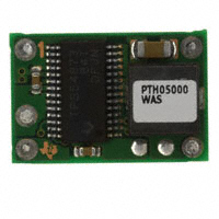
NOMINAL SIZE =
0.75 in x 0.5 in
(19,05 mm x 12,7 mm)
• Up to 6-A Output Current
• 5-V Input Voltage
• Wide-Output Voltage Adjust
(0.9 V to 3.6 V)
• Efficiencies up to 94 %
• 160 W/in³ Power Density
• On/Off Inhibit
• Under-Voltage Lockout
•
•
•
•
•
•
Output Current Limit
Pre-Bias Startup Capability
Over-Temperature Protection
Surface Mountable
Operating Temp: –40 to +85 °C
Safety Agency Approvals (Pending):
UL 1950, CSA 22.2 950, EN60950
& VDE
Description
Pin Configuration
The PTH05000 series of non-isolated
power modules are small in size and high
on performance. Using double-sided surface mount construction and synchronous
rectification technology, these regulators
deliver up to 6 A of output current while
occupying a PCB area of about half the
size of a standard postage stamp. They
are an ideal choice for applications where
space, performance and cost are important design constraints.
The series operates from an input
voltage of 5 V to provide step-down
power conversion to any output voltage
over the range, 0.9 V to 3.6 V. The output voltage of the PTH05000W is set
within this range using a single resistor.
Operating features include an on/off
inhibit, output voltage adjust (trim), an
output current limit, and over-temperature protection.
For high efficiency these parts employ
a synchronous rectifier output stage. An
output pre-bias holdoff capability ensures
that the output will not sink current during startup.
Target applications include telecom,
industrial, and general purpose circuits,
including low-power dual-voltage systems
that use a DSP, microprocessor, or ASIC.
Package options include both throughhole and surface mount configurations.
Pin
1
2
3
4
5
* Denotes negative logic:
Open
= Output On
Ground = Output Off
Standard Application
Rset = Required to set the output voltage to a value
higher than 0.9 V. See spec. table for values.
C in = Required 330 µF capacitor
C out = Optional 100 µF capacitor
1
VIN
2
PTH05000W
(Top View)
3
CIN
330 µF
(Required)
VOUT
5
4
RSET
1 %, 0.1 W
(Required)
COUT
100 µF
Electrolytic
(Optional)
Inhibit
GND
For technical support and further information visit http://power.ti.com
Function
GND
Vin
Inhibit *
Vo Adjust
Vout
GND
�PTH05000W —5-V Input
6-A, 5-V Input Non-Isolated
Wide-Output Adjust Power Module
SLTS201C – MAY 2003 – REVISED DECEMBER 2003
Ordering Information
Output Voltage (PTH05000Hxx)
Package Options (PTH05000xHH) (1)
Code
W
Code
Voltage
0.9 V – 3.6 V (Adjust)
AH
AS
Description
Pkg Ref.
Horiz. T/H
SMD, Standard (3)
(2)
(EUS)
(EUT)
Notes: (1) Add “T” to end of part number for tape and reel on SMD packages only.
(2) Reference the applicable package reference drawing for the dimensions and PC board layout
(3) “Standard” option specifies 63/37, Sn/Pb pin solder material.
Pin Descriptions
Vin: The positive input voltage power node to the module, which is referenced to common GND.
Vout: The regulated positive power output with respect
to the GND node.
GND: This is the common ground connection for the
‘Vin’ and ‘Vout’ power connections. It is also the 0 VDC
reference for the ‘Inhibit’ and ‘Vo Adjust’ control input.
Inhibit: The Inhibit pin is an open-collector/drain negative
logic input that is referenced to GND. Applying a lowlevel ground signal to this input disables the module’s
output and turns off the output voltage. When the Inhibit
control is active, the input current drawn by the regulator
is significantly reduced. If the Inhibit pin is left opencircuit, the module will produce an output whenever a
valid input source is applied.
Vo Adjust: A 0.1 W 1 % resistor must be directly connected
between this pin and the GND pin to set the output voltage
to a value higher than 0.9 V. The temperature stability
of the resistor should be 100 ppm/°C (or better). The set
point range for the output voltage is from 0.9 V to 3.6 V.
The resistor required for a given output voltage may be
calculated from the following formula. If left open circuit,
the output voltage will default to its lowest value. For
further information on output voltage adjustment, consult
the related application note.
Rset
= 10 kΩ ·
0.891 V
Vout – 0.9 V
– 3.24 kΩ
The specification table gives the preferred resistor values
for a number of standard output voltages.
For technical support and further information visit http://power.ti.com
�PTH05000W —5-V Input
6-A, 5-V Input Non-Isolated
Wide-Output Adjust Power Module
SLTS201C – MAY 2003 – REVISED DECEMBER 2003
Environmental & Absolute Maximum Ratings
Characteristics
Symbols
Conditions
Min
Typ
Max
Units
Operating Temperature Range
Solder Reflow Temperature
Storage Temperature
Over Temperature Protection
Mechanical Shock
Ta
Treflow
Ts
OTP
Over Vin Range
Surface temperature of module body or pins
—
IC junction temperature
Per Mil-STD-883D, Method 2002.3
1 msec, ½ sine, mounted
Mil-STD-883D, Method 2007.2
20-2000 Hz
–40 (i)
—
–40
—
—
150
+85
235 (ii)
+125
—
°C
°C
°C
°C
—
500
—
G’s
—
20
—
G’s
—
2
—
grams
Mechanical Vibration
Weight
Flammability
—
—
Meets UL 94V-O
Notes: (i) For operation below 0 °C the external capacitors must have stable characteristics. Use either a low ESR tantalum, Os-con, or ceramic capacitor.
(ii) During reflow of SMD package version do not elevate peak temperature of the module, pins or internal components above the stated maximum.
Electrical Specifications
Unless otherwise stated, T a =25 °C, Vin =5 V, V o =3.3 V, C in =330 µF, C out =0 µF, and Io =Io (max)
Characteristics
Symbols
Conditions
Output Current
Io
0.9 V ≤ Vo ≤3.6 V,
Input Voltage Range
Set-Point Voltage Tolerance
Temperature Variation
Line Regulation
Load Regulation
Total Output Variation
Vin
Vo tol
∆Regtemp
∆Regline
∆Regload
∆Regtot
Over Io range
Efficiency
η
Vo = 3.3 V
Vo = 2.5 V
Vo = 2.0 V
Vo = 1.8 V
Vo = 1.5 V
Vo = 1.2 V
Vo = 1.0 V
Vo ≥3.3 V
Vo ≤2.5 V
1 A/µs load step, 50 to 100 % Iomax,
Vo =1.8 V, Cout =100 µF
Recovery time
Vo over/undershoot
∆Vo = –50 mV
Vin increasing
Vin decreasing
Referenced to GND
Vo Ripple (pk-pk)
Vr
Transient Response
Current Limit
Under-Voltage Lockout
ttr
∆Vtr
Ilim
UVLO
Inhibit Control (pin 3)
Input High Voltage
Input Low Voltage
Input Low Current
VIH
VIL
IIL
Standby Input Current
Switching Frequency
External Input Capacitance
External Output Capacitance
Iin standby
ƒs
Cin
Cout
Reliability
MTBF
Min
Ta =25 °C, natural convection
Ta =60 °C, 200LFM
–40 °C
很抱歉,暂时无法提供与“PTH05000WAS”相匹配的价格&库存,您可以联系我们找货
免费人工找货