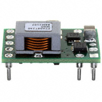
PTH08T240W, PTH08T241W
www.ti.com ................................................................................................................................................... SLTS264J – NOVEMBER 2005 – REVISED JUNE 2009
10-A, 4.5-V to 14-V INPUT, NON-ISOLATED, WIDE-OUTPUT, ADJUSTABLE POWER
MODULE WITH TurboTrans™
FEATURES
1
•
•
•
•
•
•
2
•
•
•
•
•
•
•
•
•
Up to 10-A Output Current
4.5-V to 14-V Input Voltage
Wide-Output Voltage Adjust (0.69 V to 5.5 V)
±1.5% Total Output Voltage Variation
Efficiencies up to 96%
Output Overcurrent Protection
(Nonlatching, Auto-Reset)
Operating Temperature: –40°C to 85°C
Safety Agency Approvals:
– UL/IEC/CSA-C22.2 60950-1
Prebias Startup
On/Off Inhibit
Differential Output Voltage Remote Sense
Adjustable Undervoltage Lockout
Auto-Track™ Sequencing
Ceramic Capacitor Version (PTH08T241W)
POLA™ Compatible
•
•
•
TurboTrans™ Technology
Designed to meet Ultra-Fast Transient
Requirements up to 300 A/µs
SmartSync Technology
APPLICATIONS
•
•
•
Complex Multi-Voltage Systems
Microprocessors
Bus Drivers
DESCRIPTION
The PTH08T240/241W is a high-performance 10-A rated, non-isolated power module. These modules represent
the 2nd generation of the popular PTH series power modules and include a reduced footprint and additional
features. The PTH08T241W is optimized to be used with all ceramic capacitors.
Operating from an input voltage range of 4.5 V to 14 V, the PTH08T240/241W requires a single resistor to set
the output voltage to any value over the range, 0.69 V to 5.5 V. The wide input voltage range makes the
PTH08T240/241W particularly suitable for advanced computing and server applications that utilize a loosely
regulated 8-V to 12-V intermediate distribution bus. Additionally, the wide input voltage range increases design
flexibility by supporting operation with tightly regulated 5-V, 8-V, or 12-V intermediate bus architectures.
The module incorporates a comprehensive list of features. Output over-current and over-temperature shutdown
protects against most load faults. A differential remote sense ensures tight load regulation. An adjustable
under-voltage lockout allows the turn-on voltage threshold to be customized. Auto-Track™sequencing is a
popular feature that greatly simplifies the simultaneous power-up and power-down of multiple modules in a
power system.
The PTH08T240/241W includes new patent pending technologies, TurboTrans™ and SmartSync. The
TurboTrans feature optimizes the transient response of the regulator while simultaneously reducing the quantity
of external output capacitors required to meet a target voltage deviation specification. Additionally, for a target
output capacitor bank, TurboTrans can be used to significantly improve the regulators transient response by
reducing the peak voltage deviation. SmartSync allows for switching frequency synchronization of multiple
modules, thus simplifying EMI noise suppression tasks and reducing input capacitor RMS current requirements.
The module uses double-sided surface mount construction to provide a low profile and compact footprint.
Package options include through-hole and surface mount configurations that are Pb - free and RoHS compatible.
1
2
Please be aware that an important notice concerning availability, standard warranty, and use in critical applications of Texas
Instruments semiconductor products and disclaimers thereto appears at the end of this data sheet.
TurboTrans, Auto-Track, TMS320 are trademarks of Texas Instruments.
PRODUCTION DATA information is current as of publication date.
Products conform to specifications per the terms of the Texas
Instruments standard warranty. Production processing does not
necessarily include testing of all parameters.
Copyright © 2005–2009, Texas Instruments Incorporated
�PTH08T240W, PTH08T241W
SLTS264J – NOVEMBER 2005 – REVISED JUNE 2009 ................................................................................................................................................... www.ti.com
These devices have limited built-in ESD protection. The leads should be shorted together or the device placed in conductive foam
during storage or handling to prevent electrostatic damage to the MOS gates.
PTH08T240W
SmartSync
Track
TurboTranst
10
VI
Track
2
1
TT
+Sense
SYNC
VI
VO
PTH08T240W
Inhibit
11
5
+Sense
VO
−Sense
GND
GND
3
4
VOAdj
8
+
RSET [A]
1%
0.05 W
(Required)
CI2
22 µF
(Optional)
CI
220 µF
(Required)
6
7
INH/UVLO
+
RUVLO
1%
0.05 W
(Opional)
RTT
1%
0.05 W
(Optional)
9
L
O
A
D
CO
220 µF
(Required)
−Sense
GND
GND
UDG−06005
A.
RSET required to set the output voltage to a value higher than 0.69 V. See Electrical Characteristics table.
PTH08T241W - Ceramic Capacitor Version
SmartSync
Track
TurboTranst
10
VI
Track
2
1
TT
+Sense
SYNC
VI
VO
PTH08T241W
Inhibit
11
3
RUVLO
1%
0.05 W
(Opional)
CI
200 µF
(Required)
6
5
+Sense
VO
7
INH/UVLO
GND
RTT
1%
0.05 W
(Optional)
9
−Sense
GND
4
VOAdj
8
L
O
A
D
CO
300 µF
(Required)
RSET [A]
1%
0.05 W
(Required)
−Sense
GND
GND
UDG−06005
2
A.
RSET required to set the output voltage to a value higher than 0.69 V. See Electrical Characteristics table.
B.
200 µF of ceramic or 220 µF of electrolytic input capacitance is required for proper operation.
Submit Documentation Feedback
Copyright © 2005–2009, Texas Instruments Incorporated
Product Folder Link(s): PTH08T240W PTH08T241W
�PTH08T240W, PTH08T241W
www.ti.com ................................................................................................................................................... SLTS264J – NOVEMBER 2005 – REVISED JUNE 2009
ORDERING INFORMATION
For the most current package and ordering information, see the Package Option Addendum at the end of this datasheet, or see
the TI website at www.ti.com.
DATASHEET TABLE OF CONTENTS
DATASHEET SECTION
PAGE NUMBER
ENVIRONMENTAL AND ABSOLUTE MAXIMUM RATINGS
3
ELECTRICAL CHARACTERISTICS TABLE (PTH08T240W)
4
ELECTRICAL CHARACTERISTICS TABLE (PTH08T241W)
6
TERMINAL FUNCTIONS
8
TYPICAL CHARACTERISTICS (VI = 12V)
9
TYPICAL CHARACTERISTICS (VI = 5V)
10
ADJUSTING THE OUTPUT VOLTAGE
11
INPUT & OUTPUT CAPACITOR RECOMMENDATIONS
13
TURBOTRANS™ INFORMATION
17
UNDERVOLTAGE LOCKOUT (UVLO)
22
SOFT-START POWER-UP
23
OUTPUT INHIBIT
24
OVER-CURRENT PROTECTION
25
OVER-TEMPERATURE PROTECTION
25
REMOTE SENSE
25
SYCHRONIZATION (SMARTSYNC)
26
AUTO-TRACK SEQUENCING
27
PREBIAS START-UP
30
TAPE & REEL AND TRAY DRAWINGS
32
ENVIRONMENTAL AND ABSOLUTE MAXIMUM RATINGS
(Voltages are with respect to GND)
UNIT
VTrack
Track pin voltage
TA
Operating temperature range Over VI range
Twave
Wave soldering temperature
Surface temperature of module body or
pins for 5 seconds maximum.
suffix AH
Treflow
Solder reflow temperature
Surface temperature of module body or
pins
suffix AS
235 (1)
suffix AZ
260 (1)
Tstg
Storage temperature
Storage temperature of module removed from shipping package
Tpkg
Packaging temperature
Shipping Tray or Tape and Reel storage
or bake temperature
Mechanical shock
Per Mil-STD-883D, Method 2002.3 1
msec, 1/2 sine, mounted
Mechanical vibration
–0.3 to VI + 0.3
suffix AD
(1)
260
°C
–55 to 125
45
suffix AH & AD
500
suffix AS & AZ
250
Mil-STD-883D, Method 2007.2 20-2000 Hz
Weight
Flammability
V
–40 to 85
G
15
5
grams
Meets UL94V-O
During reflow of surface mount package version do not elevate peak temperature of the module, pins or internal components above the
stated maximum.
Copyright © 2005–2009, Texas Instruments Incorporated
Product Folder Link(s): PTH08T240W PTH08T241W
Submit Documentation Feedback
3
�PTH08T240W, PTH08T241W
SLTS264J – NOVEMBER 2005 – REVISED JUNE 2009 ................................................................................................................................................... www.ti.com
ELECTRICAL CHARACTERISTICS
PTH08T240W
TA = 25°C, VI = 5 V, VO = 3.3 V, CI = 220 µF, CO = 220 µF, and IO = IO max (unless otherwise stated)
PARAMETER
TEST CONDITIONS
PTH08T240W
MIN
IO
Output current
Over VO range
25°C, natural convection
Input voltage range
VOADJ
Output voltage adjust range
Over IO range
η
1.2 < VO ≤ 3.6
4.5
14
3.6 < VO ≤ 5.5
VO + 2
14
Over IO range
0.69
±0.3
%Vo
±3
mV
Load regulation
Over IO range
±2
Total output variation
Includes set-point, line, load, –40°C ≤ TA ≤ 85°C
IO = 10 A
95%
RSET = 1.21 kΩ, VO = 3.3 V
94%
RSET = 2.38 kΩ, VO = 2.5 V
92%
RSET = 4.78 kΩ, VO = 1.8 V
90%
RSET = 7.09 kΩ, VO = 1.5 V
88%
RSET = 12.1 kΩ, VO = 1.2 V
87%
20-MHz bandwidth
Overcurrent threshold
Reset, followed by auto-recovery
Transient response
2.5 A/µs load step
50 to 100% IOmax
VO = 2.5 V
w/ TurboTrans
CO = 2000 µF, TypeC,
RTT = 0 Ω
IIL
Track input current (pin 10)
Pin to GND
dVtrack/dt
Track slew rate capability
CO ≤ CO (max)
UVLOADJ
VI increasing, RUVLO = OPEN
Adjustable Under-voltage lockout
VI decreasing, RUVLO = OPEN
(pin 11)
Hysteresis, RUVLO ≤ 52.3 kΩ
(1)
A
35
µs
VO over/undershoot
165
mV
Recovery time
130
µs
VO over/undershoot
30
4.3
3.7
fs
Switching frequency
Over VI and IO ranges, SmartSync (pin 1) to GND
fSYNC
Synchronization (SYNC)
frequency
VSYNCH
SYNC High-Level Input Voltage
VSYNCL
SYNC Low-Level Input Voltage
tSYNC
SYNC Minimum Pulse Width
(3)
µA
1
V/ms
4.45
4.2
V
0.5
Open (4)
-0.2
Input low current (IIL), Pin 11 to GND
Inhibit (pin 11) to GND, Track (pin 10) open
mV
–130
Input low voltage (VIL)
Input standby current
4
mVPP
Recovery time
Iin
(4)
%Vo
20
Input high voltage (VIH)
Inhibit control (pin 11)
(2)
85%
10
w/o TurboTrans
CO = 220 µF, TypeC
mV
±1.5
RSET = 171 Ω, VI = 8 V, VO = 5.0 V
VO Ripple (peak-to-peak)
ΔVtrTT
(3)
V
%Vo
Over VI range
ΔVtr
(2)
(2)
–40°C < TA < 85°C
ttr
(1)
±1
V
Line regulaltion
RSET = 20.8 kΩ, VO = 1.0 V
ttrTT
5.5
±0.5
A
(1)
14
Temperature variation
Efficiency
ILIM
10
4.5
Set-point voltage tolerance
VO
UNIT
MAX
0
0.69 ≤ VO ≤ 1.2
VI
TYP
0.8
V
-235
µA
5
mA
300
kHz
240
400
kHz
2
5.5
V
0.8
200
V
nSec
For output voltages ≤ 1.2 V, at nominal operating frequency, the output ripple may increase (typically 2×) when operating at input
voltages greater than (VO × 11). When using the SmartSync feature to adjust the switching frequency, see the SmartSync
Considerations section of the datasheet for further guidance.
The set-point voltage tolerance is affected by the tolerance and stability of RSET. The stated limit is unconditionally met if RSET has a
tolerance of 1% with 100 ppm/C or better temperature stability.
A low-leakage ( 3.45V please contact TI for CO and RTT values.
40
R TT +
ƪ1 * ǒCOń1100Ǔƫ
ƪǒC Oń220Ǔ * 1ƫ
(kW)
(3)
Where CO is the total output capacitance in µF. CO values greater than or equal to 1100 µF require RTT to be a
short, 0Ω. (RTT results in a negative value when CO > 1100µF).
To ensure stability, a minimum amount of output capacitance is required for a given RTT resistor value. The value
of RTT must be calculated using the minimum required output capacitance determined from the capacitor
transient response charts above.
Copyright © 2005–2009, Texas Instruments Incorporated
Product Folder Link(s): PTH08T240W PTH08T241W
Submit Documentation Feedback
19
�PTH08T240W, PTH08T241W
SLTS264J – NOVEMBER 2005 – REVISED JUNE 2009 ................................................................................................................................................... www.ti.com
PTH08T240W Type C Capacitors
12-V Input
5-V Input
30
30
20
10000
3000
200
4000
5000
6000
500
200
2000
2
10000
2
3000
3
2000
3
1000
4
300
4
4000
5000
6000
5
1000
5
10
9
8
7
6
500
10
9
8
7
6
300
Transient − mV/A
20
Transient − mV/A
WIth TurboTrans
Without TurboTrans
WIth TurboTrans
Without TurboTrans
C − Capacitance − µF
C − Capacitance − µF
Figure 16. Cap Type C, 5000 < C(µF)×ESR(mΩ) ≤ 10,000
(e.g. OS-CON)
Figure 17. Cap Type C, 5000 < C(µF)×ESR(mΩ) ≤ 10,000
(e.g. OS-CON)
Table 6. Type C TurboTrans CO Values and Required RTT Selection Table
Transient Voltage Deviation (mV)
12-V Input
5-V Input
25% load step
(2.5 A)
50% load step
(5 A)
75% load step
(7.5 A)
CO
Minimum
Required Output
Capacitance (µF)
RTT
Required
TurboTrans
Resistor (kΩ)
CO
Minimum
Required Output
Capacitance (µF)
RTT
Required
TurboTrans
Resistor (kΩ)
75
150
225
220
open
250
1300
60
120
180
270
294
330
133
45
90
135
400
68.1
480
45.3
35
70
105
580
31.6
700
21.5
30
60
90
720
20.0
860
13.7
25
50
75
950
11.8
1150
7.68
20
40
60
1300
5.23
1550
2.61
15
30
45
2000
short
2800
short
10
20
30
7400
short
exceeds limit
—
RTT Resistor Selection
The TurboTrans resistor value, RTT can be determined from the TurboTrans programming, see Equation 4 . For
VO > 3.45V please contact TI for CO and RTT values.
40
R TT +
ƪǒǒǒ5
ƪ1 * ǒCOń1980Ǔƫ
ƫ
C OǓ ) 880Ǔń1980Ǔ * 1
(kW)
(4)
Where CO is the total output capacitance in µF. CO values greater than or equal to 1980 µF require RTT to be a
short, 0Ω. (RTT results in a negative value when CO > 1980µF).
To ensure stability, the value of RTT must be calculated using the minimum required output capacitance
determined from the capacitor transient response charts above.
20
Submit Documentation Feedback
Copyright © 2005–2009, Texas Instruments Incorporated
Product Folder Link(s): PTH08T240W PTH08T241W
�PTH08T240W, PTH08T241W
www.ti.com ................................................................................................................................................... SLTS264J – NOVEMBER 2005 – REVISED JUNE 2009
TurboTrans
10
1
VI
AutoTrack
TurboTrans
+Sense
Smart
Sync
2
VI
PTH08T240W
11 Inhibit/
Prog UVLO
GND
4
6
+Sense
5
VO
VO
−Sense
3
CI
220 mF
(Required)
RTT
0 kW
9
7
VOAdj
8
L
O
A
D
CO
1320 mF
Type B
RSET
1%
0.05 W
−Sense
GND
GND
Figure 18. Typical TurboTrans™ Application
Without TurboTrans
100 mV/div
With TurboTrans
100 mV/div
2.5 A/ms
50% Load Step
Figure 19. Typical TurboTrans Waveforms
Copyright © 2005–2009, Texas Instruments Incorporated
Product Folder Link(s): PTH08T240W PTH08T241W
Submit Documentation Feedback
21
�PTH08T240W, PTH08T241W
SLTS264J – NOVEMBER 2005 – REVISED JUNE 2009 ................................................................................................................................................... www.ti.com
UNDERVOLTAGE LOCKOUT (UVLO)
The PTH08T240/241W power modules incorporate an input undervoltage lockout (UVLO). The UVLO feature
prevents the operation of the module until there is sufficient input voltage to produce a valid output voltage. This
enables the module to provide a clean, monotonic powerup for the load circuit, and also limits the magnitude of
current drawn from the regulator’s input source during the power-up sequence.
The UVLO characteristic is defined by the ON threshold (VTHD) voltage. Below the ON threshold, the Inhibit
control is overridden, and the module does not produce an output. The hysteresis voltage, which is the difference
between the ON and OFF threshold voltages, is set at 500 mV. The hysteresis prevents start-up oscillations,
which can occur if the input voltage droops slightly when the module begins drawing current from the input
source.
The UVLO feature of the PTH08T240/241W module allows for limited adjustment of the ON threshold voltage.
The adjustment is made via the Inhbit/UVLO Prog control pin (pin 11) using a single resistor (see Figure 20).
When pin 11 is left open circuit, the ON threshold voltage is internally set to its default value, which is 4.3 volts.
The ON threshold might need to be raised if the module is powered from a tightly regulated 12-V bus. Adjusting
the threshold prevents the module from operating if the input bus fails to completely rise to its specified
regulation voltage.
Equation 5 determines the value of RUVLO required to adjust VTHD to a new value. The default value is 4.3 V, and
it may only be adjusted to a higher value.
R UVLO +
9690 * ǒ137
ǒ137
VIǓ
(kW)
VIǓ * 585
(5)
Table 7 shows a chart of standard resistor values for RUVLO for different options of the on-threshold (VTHD)
voltage.
Table 7. Standard RUVLO values for Various VTHD values
VTHD (V)
5.0
5.5
6.0
6.5
7.0
7.5
8.0
8.5
9.0
9.5
10.0
10.5
11.0
RUVLO (kΩ)
88.7
52.3
37.4
28.7
23.2
19.6
16.9
14.7
13.0
11.8
10.5
9.76
8.87
PTH08T240W/241W
VI
2
VI
11 Inhibit/
UVLO Prog
GND
3
CI
4
RUVLO
GND
Figure 20. Undervoltage Lockout Adjustment Resistor Placement
22
Submit Documentation Feedback
Copyright © 2005–2009, Texas Instruments Incorporated
Product Folder Link(s): PTH08T240W PTH08T241W
�PTH08T240W, PTH08T241W
www.ti.com ................................................................................................................................................... SLTS264J – NOVEMBER 2005 – REVISED JUNE 2009
Soft-Start Power Up
The Auto-Track feature allows the power-up of multiple PTH/PTV modules to be directly controlled from the
Track pin. However in a stand-alone configuration, or when the Auto-Track feature is not being used, the Track
pin should be directly connected to the input voltage, VI (see Figure 21).
10
Track
PTH08T240W/241W
VI
2
VI
GND
3,4
CI
GND
Figure 21. Defeating the Auto-Track Function
When the Track pin is connected to the input voltage the Auto-Track function is permanently disengaged. This
allows the module to power up entirely under the control of its internal soft-start circuitry. When power up is
under soft-start control, the output voltage rises to the set-point at a quicker and more linear rate.
From the moment a valid input voltage is applied, the soft-start control introduces a short time delay (typically
2 ms–10 ms) before allowing the output voltage to rise.
VI (5 V/div)
VO (2 V/div)
II (2 A/div)
t − Time − 4 ms/div
Figure 22. Power-Up Waveform
The output then progressively rises to the module’s setpoint voltage. Figure 22 shows the soft-start power-up
characteristic of the PTH08T240/241W operating from a 12-V input bus and configured for a 3.3-V output. The
waveforms were measured with a 10-A constant current load and the Auto-Track feature disabled. The initial rise
in input current when the input voltage first starts to rise is the charge current drawn by the input capacitors.
Power-up is complete within 15 ms.
Copyright © 2005–2009, Texas Instruments Incorporated
Product Folder Link(s): PTH08T240W PTH08T241W
Submit Documentation Feedback
23
�PTH08T240W, PTH08T241W
SLTS264J – NOVEMBER 2005 – REVISED JUNE 2009 ................................................................................................................................................... www.ti.com
On/Off Inhibit
For applications requiring output voltage on/off control, the PTH08T240/241W incorporates an Inhibit control pin.
The inhibit feature can be used wherever there is a requirement for the output voltage from the regulator to be
turned off.
The power modules function normally when the Inhibit pin is left open-circuit, providing a regulated output
whenever a valid source voltage is connected to VI with respect to GND.
Figure 23 shows the typical application of the inhibit function. Note the discrete transistor (Q1). The Inhibit input
has its own internal pull-up. An external pull-up resistor should never be used with the inhibit pin. The input is not
compatible with TTL logic devices. An open-collector (or open-drain) discrete transistor is recommended for
control.
VI
2
VI
PTH08T240W/241W
11
Inhibit/
UVLO
GND
3,4
CI
1 = Inhibit
Q1
BSS 138
GND
Figure 23. On/Off Inhibit Control Circuit
Turning Q1 on applies a low voltage to the Inhibit control pin and disables the output of the module. If Q1 is then
turned off, the module executes a soft-start power-up sequence. A regulated output voltage is produced within 15
ms. Figure 24 shows the typical rise in both the output voltage and input current, following the turn-off of Q1. The
turn off of Q1 corresponds to the rise in the waveform, VINH. The waveforms were measured with a 10-A constant
current load.
VO (2 V/div)
II (2 A/div)
VINH (2 V/div)
t − Time − 4 ms/div
Figure 24. Power-Up Response from Inhibit Control
24
Submit Documentation Feedback
Copyright © 2005–2009, Texas Instruments Incorporated
Product Folder Link(s): PTH08T240W PTH08T241W
�PTH08T240W, PTH08T241W
www.ti.com ................................................................................................................................................... SLTS264J – NOVEMBER 2005 – REVISED JUNE 2009
Overcurrent Protection
For protection against load faults, all modules incorporate output overcurrent protection. Applying a load that
exceeds the regulator's overcurrent threshold causes the regulated output to shut down. Following shutdown, the
module periodically attempts to recover by initiating a soft-start power-up. This is described as a hiccup mode of
operation, whereby the module continues in a cycle of successive shutdown and power up until the load fault is
removed. During this period, the average current flowing into the fault is significantly reduced. Once the fault is
removed, the module automatically recovers and returns to normal operation.
Overtemperature Protection (OTP)
A thermal shutdown mechanism protects the module’s internal circuitry against excessively high temperatures. A
rise in the internal temperature may be the result of a drop in airflow, or a high ambient temperature. If the
internal temperature exceeds the OTP threshold, the module’s Inhibit control is internally pulled low. This turns
the output off. The output voltage drops as the external output capacitors are discharged by the load circuit. The
recovery is automatic, and begins with a soft-start power up. It occurs when the sensed temperature decreases
by about 10°C below the trip point.
The overtemperature protection is a last resort mechanism to prevent thermal stress to the regulator.
Operation at or close to the thermal shutdown temperature is not recommended and reduces the long-term
reliability of the module. Always operate the regulator within the specified safe operating area (SOA) limits for
the worst-case conditions of ambient temperature and airflow.
Differential Output Voltage Remote Sense
Differential remote sense improves the load regulation performance of the module by allowing it to compensate
for any IR voltage drop between its output and the load in either the positive or return path. An IR drop is caused
by the output current flowing through the small amount of pin and trace resistance. With the sense pins
connected, the difference between the voltage measured directly between the VO and GND pins, and that
measured at the Sense pins, is the amount of IR drop being compensated by the regulator. This should be
limited to a maximum of 0.3V. Connecting the +Sense (pin 6) to the positive load terminal improves the load
regulation at the connection point. For optimal behavior the –Sense (pin 7) must be connected to GND (pin 4)
close to the module (within 10 cm).
If the remote sense feature is not used at the load, connect the +Sense pin to VO (pin5) and connect the –Sense
pin to the module GND (pin 4).
The remote sense feature is not designed to compensate for the forward drop of nonlinear or frequency
dependent components that may be placed in series with the converter output. Examples include OR-ing
diodes, filter inductors, ferrite beads, and fuses. When these components are enclosed by the remote sense
connection they are effectively placed inside the regulation control loop, which can adversely affect the
stability of the regulator.
Copyright © 2005–2009, Texas Instruments Incorporated
Product Folder Link(s): PTH08T240W PTH08T241W
Submit Documentation Feedback
25
�PTH08T240W, PTH08T241W
SLTS264J – NOVEMBER 2005 – REVISED JUNE 2009 ................................................................................................................................................... www.ti.com
Smart Sync
Smart Sync is a feature that allows multiple power modules to be synchronized to a common frequency. Driving
the Smart Sync pins with an external oscillator set to the desired frequency, synchronizes all connected modules
to the selected frequency. The synchronization frequency can be higher or lower than the nominal switching
frequency of the modules within the range of 240 kHz to 400 kHz (see Electrical Specifications table for
frequency limits). Synchronizing modules powered from the same bus, eliminates beat frequencies reflected back
to the input supply, and also reduces EMI filtering requirements. Eliminating the low beat frequencies (usually
< 10 kHz) allows the EMI filter to be designed to attenuate only the synchronization frequency. Power modules
can also be synchronized out of phase to minimize source current loading and minimize input capacitance
requirements. Figure 25 shows a standard circuit with two modules syncronized 180° out of phase using a D
flip-flop.
0
o
Track SYNC
VI = 5 V
TT
+Sense
VI
VO1
VO
PTH08T220W
SN74LVC2G74
–Sense
INH / UVLO
GND
VOAdj
Vcc
CLR
PRE
CLK
Q
Ci1
330 mF
RSET1
C o1
220 mF
fclock = 2 X fmodules
D
Q
GND
GND
180
o
Track SYNC
TT
+Sense
VI
VO2
VO
PTH08T240W
INH / UVLO
–Sense
GND
VOAdj
Ci2
220 mF
RSET2
Co2
220 mF
GND
Figure 25. Smart Sync Schematic
26
Submit Documentation Feedback
Copyright © 2005–2009, Texas Instruments Incorporated
Product Folder Link(s): PTH08T240W PTH08T241W
�PTH08T240W, PTH08T241W
www.ti.com ................................................................................................................................................... SLTS264J – NOVEMBER 2005 – REVISED JUNE 2009
Smart Sync Considerations
Operating the PTH08T240W with a low duty cycle may increase the output voltage ripple due to pulse skipping
of the PWM controller. When operating at the nominal switching frequency, input voltages greater than (VO × 11)
may cause the output voltage ripple to increase (typically 2×).
Synchronizing to a higher frequency and operating with a low duty cycle may impact output voltage ripple. When
operating at 300 kHz, Figure 26 shows the operating region where the output voltage ripple meets the electrical
specifications and the operating region where the output voltage ripple may increase. Figure 27 shows the
operating regions for several switching frequencies. For example, a module operating at 400 kHz and an output
voltage of 1.2 V, the maximum input voltage that meets the output voltage ripple specification is 10 V. Exceeding
10 V may cause in an increase in output voltage ripple. As shown in Figure 27, operating below 6V allows
operation down to the minimum output voltage over the entire synchronization frequency range without affecting
the output voltage ripple. See the Electrical Characteristics table for the synchronization frequency range limits.
15
15
Increased VO Ripple
13
13
12
12
11
fSW = 300 kHz
10
Meets VO Ripple
Specification
9
8
fSW = 300 kHz
9
6
1.3 1.5 1.7 1.9 2.1
VO – Output Voltage – V
Figure 26. VO Ripple Regions at 300 kHz
2.3
(1) (2)
2.5
fSW = 240 kHz
8
6
1.1
fSW = 350 kHz
10
7
0.9
fSW = 400 kHz
11
7
5
0.7
(1)
(2)
14
VI – Input Voltage – V
VI – Input Voltage – V
14
5
0.7
0.9
1.1
1.3 1.5 1.7 1.9 2.1
VO – Output Voltage – V
2.3
2.5
Figure 27. VO Ripple Regions (1) (2)
Operation above a given curve may cause the output voltage ripple to increase (typically 2×).
When operating at the nominal switching frequency refer to the 300 kHz plot.
Auto-Track™ Function
The Auto-Track function is unique to the PTH/PTV family, and is available with all POLA products. Auto-Track
was designed to simplify the amount of circuitry required to make the output voltage from each module power up
and power down in sequence. The sequencing of two or more supply voltages during power up is a common
requirement for complex mixed-signal applications that use dual-voltage VLSI ICs such as the TMS320™ DSP
family, microprocessors, and ASICs.
How Auto-Track™ Works
Auto-Track works by forcing the module output voltage to follow a voltage presented at the Track control pin (1).
This control range is limited to between 0 V and the module set-point voltage. Once the track-pin voltage is
raised above the set-point voltage, the module output remains at its set-point (2). As an example, if the Track pin
of a 2.5-V regulator is at 1 V, the regulated output is 1 V. If the voltage at the Track pin rises to 3 V, the regulated
output does not go higher than 2.5 V.
When under Auto-Track control, the regulated output from the module follows the voltage at its Track pin on a
Copyright © 2005–2009, Texas Instruments Incorporated
Product Folder Link(s): PTH08T240W PTH08T241W
Submit Documentation Feedback
27
�PTH08T240W, PTH08T241W
SLTS264J – NOVEMBER 2005 – REVISED JUNE 2009 ................................................................................................................................................... www.ti.com
volt-for-volt basis. By connecting the Track pin of a number of these modules together, the output voltages follow
a common signal during power up and power down. The control signal can be an externally generated master
ramp waveform, or the output voltage from another power supply circuit (3). For convenience, the Track input
incorporates an internal RC-charge circuit. This operates off the module input voltage to produce a suitable rising
waveform at power up.
Typical Sequencing Application
The basic implementation of Auto-Track allows for simultaneous voltage sequencing of a number of Auto-Track
compliant modules. Connecting the Track inputs of two or more modules forces their track input to follow the
same collective RC-ramp waveform, and allows their power-up sequence to be coordinated from a common
Track control signal. This can be an open-collector (or open-drain) device, such as a power-up reset voltage
supervisor IC. See U3 in Figure 28.
To coordinate a power-up sequence, the Track control must first be pulled to ground potential. This should be
done at or before input power is applied to the modules. The ground signal should be maintained for at least
20 ms after input power has been applied. This brief period gives the modules time to complete their internal
soft-start initialization (4), enabling them to produce an output voltage. A low-cost supply voltage supervisor IC,
that includes a built-in time delay, is an ideal component for automatically controlling the Track inputs at power
up.
Figure 28 shows how the TL7712A supply voltage supervisor IC (U3) can be used to coordinate the sequenced
power up of PTH08T240/241W modules. The output of the TL7712A supervisor becomes active above an input
voltage of 3.6 V, enabling it to assert a ground signal to the common track control well before the input voltage
has reached the module's undervoltage lockout threshold. The ground signal is maintained until approximately 28
ms after the input voltage has risen above U3's voltage threshold, which is 4.3 V. The 28-ms time period is
controlled by the capacitor CT. The value of 2.2 µF provides sufficient time delay for the modules to complete
their internal soft-start initialization. The output voltage of each module remains at zero until the track control
voltage is allowed to rise. When U3 removes the ground signal, the track control voltage automatically rises. This
causes the output voltage of each module to rise simultaneously with the other modules, until each reaches its
respective set-point voltage.
Figure 29 shows the output voltage waveforms after input voltage is applied to the circuit. The waveforms, VO1
and VO2, represent the output voltages from the two power modules, U1 (3.3 V) and U2 (1.8 V), respectively.
VTRK, VO1, and VO2 are shown rising together to produce the desired simultaneous power-up characteristic.
The same circuit also provides a power-down sequence. When the input voltage falls below U3's voltage
threshold, the ground signal is re-applied to the common track control. This pulls the track inputs to zero volts,
forcing the output of each module to follow, as shown in Figure 30. Power down is normally complete before the
input voltage has fallen below the modules' undervoltage lockout. This is an important constraint. Once the
modules recognize that an input voltage is no longer present, their outputs can no longer follow the voltage
applied at their track input. During a power-down sequence, the fall in the output voltage from the modules is
limited by the Auto-Track slew rate capability.
Notes on Use of Auto-Track™
1. The Track pin voltage must be allowed to rise above the module set-point voltage before the module
regulates at its adjusted set-point voltage.
2. The Auto-Track function tracks almost any voltage ramp during power up, and is compatible with ramp
speeds of up to 1 V/ms.
3. The absolute maximum voltage that may be applied to the Track pin is the input voltage VI.
4. The module cannot follow a voltage at its track control input until it has completed its soft-start initialization.
This takes about 20 ms from the time that a valid voltage has been applied to its input. During this period, it
is recommended that the Track pin be held at ground potential.
5. The Auto-Track function is disabled by connecting the Track pin to the input voltage (VI). When Auto-Track is
disabled, the output voltage rises according to its softstart rate after input power has been applied.
6. The Auto-Track pin should never be used to regulate the module's output voltage for long-term, steady-state
operation.
28
Submit Documentation Feedback
Copyright © 2005–2009, Texas Instruments Incorporated
Product Folder Link(s): PTH08T240W PTH08T241W
�PTH08T240W, PTH08T241W
www.ti.com ................................................................................................................................................... SLTS264J – NOVEMBER 2005 – REVISED JUNE 2009
RTT1
U1
AutoTrack TurboTrans
Smart
+Sense
Sync
VI = 12 V
VI
VO
PTH08T240W
VO1 = 3.3 V
Inhibit/
UVLO Prog
−Sense
VOAdj
GND
+
CO1
CI1
U3
7
2
1
3
RSET1
1.62 kW
8
V CC
SENSE
RESET
5
RESIN
TL7712A
REF
RESET
6
AutoTrack TurboTrans
Smart
+Sense
Sync
GND
4
CREF
0.1 mF
CT
2.2 mF
RTT2
U2
CT
RRST
10 kW
VI
VO
PTH08T220W
Inhibit/
UVLO Prog
VO2 = 1.8 V
−Sense
GND
VOAdj
+
CO2
CI2
RSET2
4.75 kW
Figure 28. Sequenced Power Up and Power Down Using Auto-Track
VTRK (1 V/div)
VTRK (1 V/div)
VO1 (1 V/div)
VO1 (1 V/div)
VO2 (1 V/div)
VO2 (1 V/div)
t − Time − 20 ms/div
t − Time − 400 ms/div
Figure 29. Simultaneous Power Up
With Auto-Track Control
Figure 30. Simultaneous Power Down
With Auto-Track Control
Copyright © 2005–2009, Texas Instruments Incorporated
Product Folder Link(s): PTH08T240W PTH08T241W
Submit Documentation Feedback
29
�PTH08T240W, PTH08T241W
SLTS264J – NOVEMBER 2005 – REVISED JUNE 2009 ................................................................................................................................................... www.ti.com
Prebias Startup Capability
A prebias startup condition occurs as a result of an external voltage being present at the output of a power
module prior to its output becoming active. This often occurs in complex digital systems when current from
another power source is backfed through a dual-supply logic component, such as an FPGA or ASIC. Another
path might be via clamp diodes as part of a dual-supply power-up sequencing arrangement. A prebias can cause
problems with power modules that incorporate synchronous rectifiers. This is because under most operating
conditions, these types of modules can sink as well as source output current.
The PTH family of power modules incorporate synchronous rectifiers, but does not sink current during startup(1),
or whenever the Inhibit pin is held low. However, to ensure satisfactory operation of this function, certain
conditions must be maintained(2). Figure 31 shows an application demonstrating the prebias startup capability.
The startup waveforms are shown in Figure 32. Note that the output current (IO) is negligible until the output
voltage rises above the voltage backfed through the intrinsic diodes.
The prebias start-up feature is not compatible with Auto-Track. When the module is under Auto-Track control, it
sinks current if the output voltage is below that of a back-feeding source. To ensure a pre-bias hold-off one of
two approaches must be followed when input power is applied to the module. The Auto-Track function must
either be disabled(3), or the module’s output held off (for at least 50 ms) using the Inhibit pin. Either approach
ensures that the Track pin voltage is above the set-point voltage at start up.
1. Startup includes the short delay (approximately 10 ms) prior to the output voltage rising, followed by the rise
of the output voltage under the module’s internal soft-start control. Startup is complete when the output
voltage has risen to either the set-point voltage or the voltage at the Track pin, whichever is lowest.
2. To ensure that the regulator does not sink current when power is first applied (even with a ground signal
applied to the Inhibit control pin), the input voltage must always be greater than the output voltage throughout
the power-up and power-down sequence.
3. The Auto-Track function can be disabled at power up by immediately applying a voltage to the module’s
Track pin that is greater than its set-point voltage. This can be easily accomplished by connecting the Track
pin to VI.
3.3 V
VI = 5 V
Track
+Sense
PTH08T240W
VI
Inhibit GND
Vadj
Vo = 2.5 V
VO
Io
-Sense
VCCIO
VCORE
+
+
CI
CO
RSET
2.37 kW
ASIC
Figure 31. PreBias Startup Application Circuit
30
Submit Documentation Feedback
Copyright © 2005–2009, Texas Instruments Incorporated
Product Folder Link(s): PTH08T240W PTH08T241W
�PTH08T240W, PTH08T241W
www.ti.com ................................................................................................................................................... SLTS264J – NOVEMBER 2005 – REVISED JUNE 2009
VIN (1 V/div)
VO (1 V/div)
IO (2 A/div)
t - Time - 4 ms/div
Figure 32. Prebias Startup Waveforms
Copyright © 2005–2009, Texas Instruments Incorporated
Product Folder Link(s): PTH08T240W PTH08T241W
Submit Documentation Feedback
31
�PTH08T240W, PTH08T241W
SLTS264J – NOVEMBER 2005 – REVISED JUNE 2009 ................................................................................................................................................... www.ti.com
TAPE AND REEL
32
Submit Documentation Feedback
Copyright © 2005–2009, Texas Instruments Incorporated
Product Folder Link(s): PTH08T240W PTH08T241W
�PTH08T240W, PTH08T241W
www.ti.com ................................................................................................................................................... SLTS264J – NOVEMBER 2005 – REVISED JUNE 2009
TRAY
Copyright © 2005–2009, Texas Instruments Incorporated
Product Folder Link(s): PTH08T240W PTH08T241W
Submit Documentation Feedback
33
�PACKAGE OPTION ADDENDUM
www.ti.com
6-Feb-2022
PACKAGING INFORMATION
Orderable Device
Status
(1)
Package Type Package Pins Package
Drawing
Qty
Eco Plan
(2)
Lead finish/
Ball material
MSL Peak Temp
Op Temp (°C)
(3)
Device Marking
(4/5)
(6)
PTH08T240WAD
ACTIVE
ThroughHole Module
EBS
11
49
RoHS Exempt
& Green
SN
N / A for Pkg Type
-40 to 85
PTH08T240WAH
ACTIVE
ThroughHole Module
EBS
11
49
RoHS Exempt
& Green
SN
N / A for Pkg Type
-40 to 85
PTH08T240WAS
ACTIVE
Surface
Mount Module
EBT
11
49
Non-RoHS
& Green
SNPB
Level-1-235C-UNLIM/
Level-3-260C-168HRS
-40 to 85
PTH08T240WAST
ACTIVE
Surface
Mount Module
EBT
11
250
Non-RoHS
& Green
SNPB
Level-1-235C-UNLIM/
Level-3-260C-168HRS
-40 to 85
PTH08T240WAZ
ACTIVE
Surface
Mount Module
BBT
11
49
RoHS (In
Work) & Green
SNAGCU
Level-3-260C-168 HR
-40 to 85
PTH08T240WAZT
ACTIVE
Surface
Mount Module
BBT
11
250
RoHS (In
Work) & Green
SNAGCU
Level-3-260C-168 HR
-40 to 85
PTH08T241WAD
ACTIVE
ThroughHole Module
EBS
11
49
RoHS Exempt
& Green
SN
N / A for Pkg Type
-40 to 85
PTH08T241WAS
ACTIVE
Surface
Mount Module
EBT
11
49
Non-RoHS
& Green
SNPB
Level-1-235C-UNLIM/
Level-3-260C-168HRS
-40 to 85
PTH08T241WAST
ACTIVE
Surface
Mount Module
EBT
11
250
Non-RoHS
& Green
SNPB
Level-1-235C-UNLIM/
Level-3-260C-168HRS
-40 to 85
PTH08T241WAZ
ACTIVE
Surface
Mount Module
BBT
11
49
RoHS (In
Work) & Green
SNAGCU
Level-3-260C-168 HR
-40 to 85
PTH08T241WAZT
ACTIVE
Surface
Mount Module
BBT
11
250
RoHS (In
Work) & Green
SNAGCU
Level-3-260C-168 HR
-40 to 85
(1)
The marketing status values are defined as follows:
ACTIVE: Product device recommended for new designs.
LIFEBUY: TI has announced that the device will be discontinued, and a lifetime-buy period is in effect.
NRND: Not recommended for new designs. Device is in production to support existing customers, but TI does not recommend using this part in a new design.
PREVIEW: Device has been announced but is not in production. Samples may or may not be available.
OBSOLETE: TI has discontinued the production of the device.
(2)
RoHS: TI defines "RoHS" to mean semiconductor products that are compliant with the current EU RoHS requirements for all 10 RoHS substances, including the requirement that RoHS substance
do not exceed 0.1% by weight in homogeneous materials. Where designed to be soldered at high temperatures, "RoHS" products are suitable for use in specified lead-free processes. TI may
reference these types of products as "Pb-Free".
RoHS Exempt: TI defines "RoHS Exempt" to mean products that contain lead but are compliant with EU RoHS pursuant to a specific EU RoHS exemption.
Addendum-Page 1
Samples
�PACKAGE OPTION ADDENDUM
www.ti.com
6-Feb-2022
Green: TI defines "Green" to mean the content of Chlorine (Cl) and Bromine (Br) based flame retardants meet JS709B low halogen requirements of