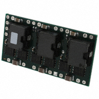
PTH12040W
www.ti.com............................................................................................................................................... SLTS237G – DECEMBER 2004 – REVISED MARCH 2009
50-A, 8-V TO 14-V INPUT, NON-ISOLATED WIDE-OUTPUT
ADJUST POWER MODULE
FEATURES
APPLICATIONS
•
•
•
•
•
•
•
•
1
2
•
•
•
•
•
•
•
•
50-A Output Current
8-V to 14-V Input Voltage
Wide-Output Voltage Adjust (0.8 V to 5.5 V)
Efficiencies up to 96%
On/Off Inhibit
Differential Output Sense
Output Overcurrent Protection
(Nonlatching, Auto-Reset)
Overtemperature Protection
Auto-Track™ Sequencing
Start Up Into Output Prebias
Margin Up/Down Controls
Operating Temperature: –40°C to 85°C
Multi-Phase, Switch-Mode Topology
Programmable Undervoltage Lockout (UVLO)
Safety Agency Approvals:
UL/cUL 60950, EN60950, VDE
Advanced Computing and Server Applications
NOMINAL SIZE =
2.05 in x 1.05 in
(52 mm x 26,7 mm)
DESCRIPTION
The PTH12040W is a high-performance 50-A rated, non-isolated, power module, which uses the latest
multiphase switched-mode topology. This provides a small, ready-to-use module, that can power the most densly
populated multiprocessor systems.
Operating from an input voltage range of 8 V to 14 V, the PTH12040W requires a single resistor to set the output
voltage to any value over the range, 0.8 V to 5.5 V. The wide input voltage range makes the PTH12040W
particularly suitable for advanced computing and server applications that utilize a loosely regulated 12-V
intermediate distribution bus.
The modules incorporate a comprehensive list of features. They include on/off inhibit and margin up/down
controls. A differential remote output voltage sense ensures tight load regulation, and an output overcurrent and
overtemperature shutdown protect against most load faults. The programmable under-voltage lockout allows the
turn-on and turn-off voltage thresholds to be customized.
The PTH12040W incorporates Auto-Track™. The Auto-Track feature of the PTH family allows the outputs of
multiple modules to track a common voltage during power up and power down transitions. This simplifies power
up and power down supply-voltage sequencing in a power supply system.
The modules use double-sided surface mount construction to provide a low profile and compact footprint.
Package options include both through-hole and surface mount configurations.
1
2
Please be aware that an important notice concerning availability, standard warranty, and use in critical applications of Texas
Instruments semiconductor products and disclaimers thereto appears at the end of this data sheet.
Auto-Track, POLA, TMS320 are trademarks of Texas Instruments.
PRODUCTION DATA information is current as of publication date.
Products conform to specifications per the terms of the Texas
Instruments standard warranty. Production processing does not
necessarily include testing of all parameters.
Copyright © 2004–2009, Texas Instruments Incorporated
�PTH12040W
SLTS237G – DECEMBER 2004 – REVISED MARCH 2009............................................................................................................................................... www.ti.com
These devices have limited built-in ESD protection. The leads should be shorted together or the device placed in conductive foam
during storage or handling to prevent electrostatic damage to the MOS gates.
STANDARD APPLICATION
Track
Margin Down
Margin Up
2
VI
+
CI
560 mF
(Required)
19
20
18
Margin Up
Margin Down
Track
+Sense
+Sense 11
VI
VO
4
VI
6
VI
8
UVLO Prog
9
VO
VO 12
PTH12040W
VO 15
Inhibit
Track
GND GNDGND
7
1
3
5
–Sense 14
GND GND GND VOAdjust
10
13
16
+
+
CO1
330 mF
(Required)
17
RSET
1%
0.05 W
L
O
A
D
CO2
330 mF
(Required)
–Sense
Inhibit
GND
GND
UDG-08112
A.
RSET = Required to set the output voltage higher than the minimum value (see the elcetrical characheristics for
values.)
B.
CI = Required 560-µF electrolytic capacitor. 1000 µF recommended.
C.
CO = Required 660-µF (or 680 µF) electrolytic capacitor.
ORDERING INFORMATION
For the most current package and ordering information, see the Package Option Addendum at the end of this datasheet, or see
the TI website at www.ti.com.
ABSOLUTE MAXIMUM RATINGS
over operating free-air temperature range (unless otherwise noted)
UNIT
Signal input voltages
Track control (pin 18)
–0.3 V to VI + 0.3 V
TA
Operating temperature range over VI range
–40°C to 85°C
Twave
Wave solder
temperature
Surface temperature of module body or pins
(5 seconds maximum)
Treflow
Solder reflow
temperature
Surface temperature of module body or pins
Tstg
Storage temperature
Storage temperature of module removed from shipping package
Tpkg
Packaging temperature Shipping Tray storage or bake temperature
45°C
Mechanical shock
Per Mil-STD-883D, Method 2002.3, 1 msec, 1/2 Sine, mounted
500 G
Mechanical vibration
Mil-STD-883D, Method 2007.2, 20–2000 Hz
Weight
Flammability
(1)
2
PTH12040WAH
260°C
(1)
PTH12040WAS
235°C
(1)
PTH12040WAZ
260°C
(1)
PTH12040WAD
–55°C to 125°C
15 G
17 grams
Meets UL94V-O
During the soldering process, do not elevate peak temperature of the module, pins, or internal components above the stated maximum.
Submit Documentation Feedback
Copyright © 2004–2009, Texas Instruments Incorporated
Product Folder Link(s): PTH12040W
�PTH12040W
www.ti.com............................................................................................................................................... SLTS237G – DECEMBER 2004 – REVISED MARCH 2009
ELECTRICAL CHARACTERISTICS
TA = 25°C, VI = 12 V, VO = 3.3 V, CI = 1000 µF, CO = 660 µF, and IO = IOmax (unless otherwise stated)
PARAMETER
TEST CONDITIONS
MIN
MAX
UNIT
0
TYP
50 (1)
A
8 (2)
14
IO
Output current
60°C, 200 LFM airflow
VI
Input voltage range
Over IO range
VOtol
Set-point voltage tolerance
ΔRegtemp
Temperature variation
–40°C < TA < 85°C
±0.5
%VO
ΔRegline
Line regulation
Over VI range
±5
mV
ΔRegload
Load regulation
Over IO range
±5
ΔRegtot
Total output variation
Includes set-point, line, load, –40°C ≤ TA ≤ 85°C
ΔRegadj
Output adjust range
η
Efficiency
±2 (3)
0.8
IO = 35 A
RSET = 205 Ω, VO = 5.0 V
96%
%VO
5.5 (2)
V
RSET = 1.5 kΩ, VO = 3.3 V
95%
93%
RSET = 4.99 kΩ, VO = 2.0 V
92%
RSET = 6.34 kΩ, VO = 1.8 V
91%
RSET = 9.76 kΩ, VO = 1.5 V
90%
RSET = 18.2 kΩ, VO = 1.2 V
88%
RSET = 38.3 kΩ, VO = 1.0 V
86%
RSET = open circuit, VO = 0.8 V
82%
All voltages
15
mVpp
95
A
Recovery time
70
µSec
VO over/undershoot
150
mV
VO ripple (pk-pk)
20 MHz bandwidth
IOtrip
Overcurrent threshold
Reset, followed by auto-recovery
Transient response
1 A/µs load step, 50 to 100% IOmax, CO = 660 µF
trr
VOadj
Margin up/down adjust
With Margin up/down control
±5%
IILmargin
Margin input current
Pin to GND
–8 (4)
IILtrack
Track input current (pin 18)
Pin to GND
dVtrack/dt
Track slew rate capability
|VTRACK – VO | ≤ 50 mV and VTRACK < VO(nom)
UVLO
Undervoltage lockout
Pin 8 open
Inhibit control (pin 7)
mV
±3 (3)
RSET = 3.01 kΩ, VO = 2.5 V
VR
ΔVtr
µA
–0.10 (5)
1
On-threshold
7.5 (6)
Hysterisis
1 (6)
2.5
Open (7)
VIL
Input low voltage
–0.2
0.5
IILinhibit
Input low current
Pin to GND
0.5
IIinh
Input standby current
Inhibit (pin 7) to GND
35
fs
Switching frequency
Over VI and IO ranges
CI
External input capacitance
(6)
(7)
(8)
V/ms
Referenced to GND
Input high voltage
(4)
(5)
mA
V
VIH
(1)
(2)
(3)
V
%VO
0.9
1.05
560 (8)
1000
V
mA
mA
1.2
MHz
µF
See SOA curves or consult factory for appropriate derating.
When the set-point voltage is adjusted higher than 3.6 V, a 10-V minimum input voltage is recommended.
The set-point voltage tolerance is affected by the tolerance of RSET. The stated limit is unconditionally met if RSET has a tolerance of 1%
with 100 ppm/°C or better temperature stability.
A small, low-leakage (