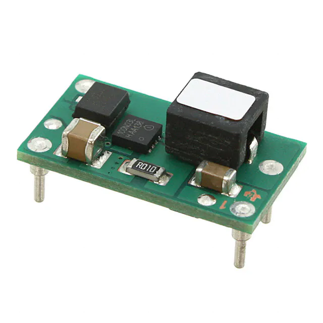
PTN04050C
www.ti.com
SLTS251A – SEPTEMBER 2005 – REVISED FEBRUARY 2011
12-W, 3.3/5-V INPUT, WIDE OUTPUT ADJUSTABLE BOOST CONVERTER
Check for Samples: PTN04050C
FEATURES
APPLICATIONS
•
•
•
1
•
•
•
•
Up to 12 W Output Power
Wide Input Voltage Range
(2.95 V to 5.5 V)
Wide Output Voltage Adjust
(5 V to 15 V)
High Efficiency (Up to 90%)
Operating Temperature: –40°C to 85°C
Surface Mount Package Available
Telecommunications, Instrumentation,
and General-Purpose Applications
DESCRIPTION
The PTN04050C is a 4-pin boost-voltage regulator product. In new designs it should be considered in place of
the PT5040 series of positive step-up products. The PTN04050C is smaller and lighter than its predecessors,
and has either similar or improved electrical performance characteristics. The case-less, double-sided package,
also exhibits improved thermal characteristics, and is compatible with TI's roadmap for RoHS and lead-free
compliance.
Operating over a 2.95V to 5.5V input range, the PTN04050C provides high-efficiency, step-up voltage conversion
for loads of up to 12W. The output voltage is set using a single external resistor. The PTN04050C may be set to
any value within the range, 5V to 15V. The output voltage of the PTN04050C can be as little as 0.5V higher than
the input, allowing an output voltage of 5V, with an input voltage of 4.5V.
The PTN04050C modules are suited to a wide variety of general-purpose applications that operate off 3.3-V or 5V dc power.
STANDARD APPLICATION
VI
1
2
4
PTN04050C
(Top View)
3
CI*
100 mF
Electrolytic
(Required)
VO
RSET#
0.1 W, 1%
(Required)
GND
CO*
100 mF
Electrolytic
(Required)
GND
* See the Application Information section for capacitor recommendations.
# See the Application Information section for RSET values.
1
Please be aware that an important notice concerning availability, standard warranty, and use in critical applications of
Texas Instruments semiconductor products and disclaimers thereto appears at the end of this data sheet.
PRODUCTION DATA information is current as of publication date.
Products conform to specifications per the terms of the Texas
Instruments standard warranty. Production processing does not
necessarily include testing of all parameters.
Copyright © 2005–2011, Texas Instruments Incorporated
�PTN04050C
SLTS251A – SEPTEMBER 2005 – REVISED FEBRUARY 2011
www.ti.com
These devices have limited built-in ESD protection. The leads should be shorted together or the device placed in conductive foam
during storage or handling to prevent electrostatic damage to the MOS gates.
ORDERING INFORMATION
For the most current package and ordering information, see the Package Option Addendum at the end of this datasheet, or see
the TI website at www.ti.com.
ABSOLUTE MAXIMUM RATINGS
(1)
over operating free-air temperature range unless otherwise noted
all voltages with respect to GND (pin 1),
UNIT
TA
Operating free-air temperature
Over VI range
Leaded temperature (H suffix)
5 seconds
Solder reflow temperature (S suffix)
Surface temperature of module body or pins
235°C
Solder reflow temperature (Z suffix) (3)
Surface temperature of module body or pins
260°C (3)
Tstg
Storage temperature
PO
Output power
(1)
(2)
(3)
–40°C to 85°C
260°C
(2)
–55°C to 125°C
12 W
Stresses beyond those listed under absolute maximum ratings may cause permanent damage to the device. These are stress ratings
only, and functional operation of the device at these or any other conditions beyond those indicated under recommended operating
conditions is not implied. Exposure to absolute-maximum-rated conditions for extended periods may affect device reliability.
This model is NOT compatible with surface-mount reflow solder process.
Moisture Sensitivity Level (MSL) Rating Level-3-260C-168HR
RECOMMENDED OPERATING CONDITIONS
MIN
MAX
VI
Input voltage
2.95
5.5
UNIT
V
TA
Operating free-air temperature
–40
85
°C
PACKAGE SPECIFICATIONS
PTN04050Cx (Suffix AH, AS, and AZ)
Weight
2.8 grams
Flammability
Meets UL 94 V-O
Mechanical shock
Per Mil-STD-883D, Method 2002.3, 1 ms, 1/2 sine,
mounted
Mechanical vibration
Mil-STD-883D, Method 2007.2, 20-2000 Hz
(1)
2
500 G
(1)
Horizontal T/H (suffix AH)
20 G
(1)
Horizontal SMD (suffix AS and AZ)
15 G
(1)
Qualification limit.
Submit Documentation Feedback
Copyright © 2005–2011, Texas Instruments Incorporated
Product Folder Links: PTN04050C
�PTN04050C
www.ti.com
SLTS251A – SEPTEMBER 2005 – REVISED FEBRUARY 2011
ELECTRICAL CHARACTERISTICS
operating at 25°C free-air temperature, VI = 5 V, VO = 12 V, IO = IO (max), CI = 100 μF, CO = 100 μF (unless otherwise noted)
PARAMETER
TEST CONDITIONS
PTN04050C
MIN
Over VI Range
IO
Output current
VI
Input voltage range
η
MAX
0.1
(1)
0.8
VO = 12 V
0.1
(1)
1.0
VO = 9 V
0.1
(1)
1.3
VO = 5 V
0.1
(1)
Over IO range
UNIT
A
2.4
2.95
Output adjust range
VO
TYP
VO = 15 V
5.5
5
±2
(2)
V
15
V
(3)
%VO
Set-point voltage tolerance
TA = 25°C
Temperature variation
–40°C to 85°C
Line regulation
Over VI range
±0.5
%VO
Load regulation
Over IO range
±0.5
%VO
Total Output Voltage
Variation
Includes set point, line, load
–40°C < TA < 85°C
(3)
%VO
3
%VO
±0.5
Efficiency
Output voltage ripple
(peak-to-peak)
%VO
±3
VI = 5 V, RSET = 60.4 Ω, VO = 15 V
88%
VI = 5 V, RSET = 1.33 kΩ, VO = 12 V
89%
VI = 5 V, RSET = 4.53 kΩ, VO = 9 V
90%
VI = 3.3 V, RSET = OPEN, VO = 5 V
87%
20-MHz bandwith
1.5
1 A/μs load step from 50% to 100% IOmax
Recovery time
500
μs
VO over/undershoot
2.5
%VO
Transient response
Ilim
Current limit
Iir
Inrush current
tir
Inrush current time
duration
FS
Switching frequency
CI
150 (4)
Over VI and IO ranges
External input capacitance
External output
capacitance
Calculated reliability
450
Per Telcordia SR-332, 50% stress,
TA = 40°C, ground benign
525
ms
600
100
(6)
100
(7)
560
(8)
0
100
(9)
Ceramic
Equivalent series resistance (nonceramic)
MTBF
A
1
Nonceramic
CO
%IOmax
2 (5)
10
kHz
μF
μF
(10)
mΩ
8.9
106 Hr
(1)
(2)
Operation at no load is not recommended.
The maximum VI is 5.5V or (VO- 0.5V) whichever is less. If the difference in VO to VIN is ≥ 0.5V and ≤ 1.4V, the device will operate in
asynchronous mode. In this condition, there may be multiple output voltage ripple frequencies and the total output voltage variation may
increase by up to 2%.
(3) The set-point voltage tolerance is affected by the tolerance and stability of RSET. The stated limit is unconditionally met if RSET has a
tolerance of 1% with 100 ppm/°C or better temperature stability.
(4) Boost-topology switching regulators are not short-circuit protected.
(5) The inrush current stated is in addition to the normal input current for the associated output load.
(6) An external input capacitor is required across the input (VI and GND) for proper operation. See the application information for further
guidance.
(7) An external output capacitance is required for proper operation. See the application information for further guidance.
(8) The minimum ESR limitation may result in a lower value for the output capacitance. See the application information for further guidance.
(9) When using ceramic capacitors equivalent to 100 μF, a 100 μF bulk electrolytic is also required.
(10) This is the minimum ESR for all the electrolytic (nonceramic) output capacitance. Use 17 mΩ as the minimum when using maximum
ESR values to calculate.
Submit Documentation Feedback
Copyright © 2005–2011, Texas Instruments Incorporated
Product Folder Links: PTN04050C
3
�PTN04050C
SLTS251A – SEPTEMBER 2005 – REVISED FEBRUARY 2011
www.ti.com
PIN ASSIGNMENT
1
2
4
PTN04050C
(Top View)
3
PIN FUNCTIONS
PIN
NAME
NO.
I/O
DESCRIPTION
This is the common ground connection for the VI and VO power connections. It is also the 0 Vdc
reference for the VO Adjust control input.
GND
1
I/O
VI
2
I
The positive input voltage power node to the module, which is referenced to common GND.
VO Adjust
3
I
A 1% resistor must be connected between this pin and GND (pin 1) to set the output voltage. If left
open-circuit, the output voltage will default to its minimum adjust value. The temperature stability of the
resistor should be 100 ppm/°C (or better). The set-point range is 5 V to 15 V. The standard resistor
value for a number of common output voltages is provided in the application information.
VO
4
O
The regulated positive power output with respect to the GND node.
4
Submit Documentation Feedback
Copyright © 2005–2011, Texas Instruments Incorporated
Product Folder Links: PTN04050C
�PTN04050C
www.ti.com
SLTS251A – SEPTEMBER 2005 – REVISED FEBRUARY 2011
TYPICAL CHARACTERISTICS (3.3-V INPUT) (1)
EFFICIENCY
vs
OUTPUT CURRENT
OUTPUT VOLTAGE RIPPLE
vs
OUTPUT CURRENT
90
VO = 9 V
VO = 12 V
VO = 15 V
70
VO = 15 V
150
120
VO = 9 V
90
VO = 12 V
60
VO = 5 V
30
VO = 9 V
1.2
0.8
0
0.8
0.4
1.6
1.2
2
2.4
0
0
0.8
0.4
1.2
1.6
2
2.4
0
1.6
1.2
2
IO - Output Current - A
Figure 1.
Figure 2.
Figure 3.
TEMPERATURE DERATING
vs
OUTPUT CURRENT
TEMPERATURE DERATING
vs
OUTPUT CURRENT
TEMPERATURE DERATING
vs
OUTPUT CURRENT
Ambient Temperature - °C
80
Airflow:
70
200 LFM
60
100 LFM
50
60 LFM
Nat conv
40
VO = 5 V
30
90
80
Airflow:
200 LFM
70
100 LFM
60
60 LFM
50
Nat conv
40
VO = 9 V
1
1.5
2
20
2.5
80
Airflow:
200 LFM
70
100 LFM
60
60 LFM
50
Nat conv
40
VO = 12 V
30
30
0.5
2.4
IO - Output Current - A
90
0
0.8
0.4
IO - Output Current - A
90
20
VO = 5 V
0.4
0
60
VO = 12 V
1.6
Ambient Temperature - °C
Efficiency - %
2
VO = 15 V
PD - Power Dissipation - W
VO - Output Voltage Ripple - VPP (mV)
VO = 5 V
Ambient Temperature - °C
POWER DISSIPATION
vs
OUTPUT CURRENT
180
100
80
(2)
0
0.3
IO - Output Current - A
0.6
0.9
1.2
Figure 4.
20
0
0.2
0.4
0.6
0.8
1
IO - Output Current - A
IO - Output Current - A
Figure 5.
Figure 6.
TEMPERATURE DERATING
vs
OUTPUT CURRENT
Ambient Temperature - °C
90
80
Airflow:
200 LFM
70
100 LFM
60
60 LFM
50
Nat conv
40
VO = 15 V
30
20
0
0.2
0.4
0.6
0.8
IO - Output Current - A
Figure 7.
(1)
(2)
The electrical characteristic data has been developed from actual products tested at 25°C. This data is considered typical for the
converter. Applies to Figure 1, Figure 2, and Figure 3.
The Safe Operating Area curves represent the conditions at which internal components are at or below the manufacturer's maximum
operating temperatures. Derating limits apply to modules soldered directly to a 100 mm x 100 mm double-sided PCB with 2 oz. copper.
Applies to Figure 4, Figure 5, Figure 6, and Figure 7.
Submit Documentation Feedback
Copyright © 2005–2011, Texas Instruments Incorporated
Product Folder Links: PTN04050C
5
�PTN04050C
SLTS251A – SEPTEMBER 2005 – REVISED FEBRUARY 2011
www.ti.com
TYPICAL CHARACTERISTICS (5-V INPUT) (1)
EFFICIENCY
vs
OUTPUT CURRENT
OUTPUT VOLTAGE RIPPLE
vs
OUTPUT CURRENT
90
VO = 12 V
VO = 15 V
70
VO = 15 V
120
VO = 12 V
90
60
VO = 9 V
30
0
60
0
0.2
0.4
0.8
0.6
1
1.2
0
0.2
IO - Output Current - A
0
0.2
0.4
0.8
0.6
1
1.2
IO - Output Current - A
TEMPERATURE DERATING
vs
OUTPUT CURRENT
TEMPERATURE DERATING
vs
OUTPUT CURRENT
TEMPERATURE DERATING
vs
OUTPUT CURRENT
90
80
Airflow:
200 LFM
70
Ambient Temperature - °C
Ambient Temperature - °C
0
1.2
90
100 LFM
60 LFM
60
Nat conv
50
40
VO = 9 V
80
Airflow:
200 LFM
70
100 LFM
60
60 LFM
50
Nat conv
40
VO = 12 V
30
0
VO = 9 V
0.3
Figure 10.
0.3
0.6
0.9
1.2
Figure 11.
6
1
0.6
Figure 9.
IO - Output Current - A
(2)
0.8
0.6
0.9
Figure 8.
30
(1)
0.4
VO = 12 V
1.2
IO - Output Current - A
90
80
VO = 15 V
1.5
150
Ambient Temperature - °C
Efficiency - %
1.8
PD - Power Dissipoation - W
VO - Output Voltage Ripple - VPP (mV)
VO = 9 V
20
POWER DISSIPATION
vs
OUTPUT CURRENT
180
100
80
(2)
20
Airflow:
200 LFM
70
100 LFM
60
60 LFM
50
Nat conv
40
VO = 15 V
30
0
0.2
0.4
0.6
0.8
IO - Output Current - A
Figure 12.
1
20
0
0.2
0.4
0.6
0.8
IO - Output Current - A
Figure 13.
The electrical characteristic data has been developed from actual products tested at 25°C. This data is considered typical for the
converter. Applies to Figure 8, Figure 9, and Figure 10.
The Safe Operating Area curves represent the conditions at which internal components are at or below the manufacturer's maximum
operating temperatures. Derating limits apply to modules soldered directly to a 100-mm x 100-mm, double-sided PCB with 2 oz. copper.
Applies to Figure 11, Figure 12, and Figure 13.
Submit Documentation Feedback
Copyright © 2005–2011, Texas Instruments Incorporated
Product Folder Links: PTN04050C
�PTN04050C
www.ti.com
SLTS251A – SEPTEMBER 2005 – REVISED FEBRUARY 2011
APPLICATION INFORMATION
Adjusting the Output Voltage of the PTN04050C Wide-Output Adjust Power Modules
General
A resistor must be connected between the VO Adjust control (pin 3) and GND (pin 1) to set the output voltage of
the PTN04050C product. The adjustment range is from 5 V to 15 V. If pin 3 is left open, the output voltage
defaults to the lowest value.
Table 1 gives the standard resistor value for several common voltages, along with the actual output voltage that
the value provides. For other output voltages, the value of the required resistor can be calculated using
Equation 1. Alternatively, RSET can be simply selected from the range of values given in Table 2. Figure 14
shows the placement of the required resistor.
RSET = 15 kW ´
2V
VO - 5 V
- 2.94 kW
(1)
Table 1. Standard Values of RSET for Common Output
Voltages
VO
(Required)
RSET
(Standard Value)
VO
(Actual)
5.0 V
Open
5.00 V
9.0 V
4.53 kΩ
9.01 V
12.0 V
1.33 kΩ
12.03 V
15.0 V
60.4 Ω
14.99 V
VI
2
PTN04050C
VO
VI
VO
Adj
GND
1
CI
100 mF
(Required)
4
3
RSET
0.01 W
1%
GND
CO
100 mF
(Required)
GND
(1)
A 0.05-W rated resistor may be used. The tolerance should be 1%, with a temperature stability of 100 ppm/°C (or
better). Place the resistor as close to the regulator as possible. Connect the resistor directly between pins 3 and 1
using dedicated PCB traces.
(2)
Never connect capacitors from VO Adjust to GND or VO . Any capacitance added to the VO Adjust pin affects the
stability of the regulator.
Figure 14. PTN04050C VO Adjust Resistor Placement
Submit Documentation Feedback
Copyright © 2005–2011, Texas Instruments Incorporated
Product Folder Links: PTN04050C
7
�PTN04050C
SLTS251A – SEPTEMBER 2005 – REVISED FEBRUARY 2011
www.ti.com
Table 2. PTN04050C Output Voltage Set-Point Resistor Values
8
VO
RSET
VO
RSET
VO
RSET
5V
Open
10 V
3.06 kΩ
12.6 V
1.01 kΩ
5.2 V
147 kΩ
10.1 V
2.94 kΩ
12.7 V
956 Ω
5.4 V
72 kΩ
10.2 V
2.83 kΩ
12.8 V
906 Ω
5.6 V
47 kΩ
10.3 V
2.72 kΩ
12.9 V
857 Ω
5.8 V
34.5 kΩ
10.4 V
2.62 kΩ
13 V
810 Ω
6V
27 kΩ
10.5 V
2.52 kΩ
13.1 V
764 Ω
6.2 V
22 kΩ
10.6 V
2.42 kΩ
13.2 V
719 Ω
6.4 V
18.5 kΩ
10.7 V
2.32 kΩ
13.3 V
674 Ω
6.6 V
15.8 kΩ
10.8 V
2.23 kΩ
13.4 V
631 Ω
6.8 V
13.7 kΩ
10.9 V
2.15 kΩ
13.5 V
589 Ω
7V
12 kΩ
11 V
2.06 kΩ
13.6 V
548 Ω
7.2 V
10.7 kΩ
11.1 V
1.98 kΩ
13.7 V
508 Ω
7.4 V
9.56 kΩ
11.2 V
1.89 kΩ
13.8 V
469 Ω
7.6 V
8.60 kΩ
11.3 V
1.82 kΩ
13.9 V
431 Ω
7.8 V
7.77 kΩ
11.4 V
1.75 kΩ
14 V
393 Ω
8V
7.06 kΩ
11.5 V
1.67 kΩ
14.1 V
357 Ω
8.2 V
6.44 kΩ
11.6 V
1.60 kΩ
14.2 V
321 Ω
8.4 V
5.88 kΩ
11.7 V
1.54 kΩ
14.3 V
286 Ω
8.6 V
5.39 kΩ
11.8 V
1.47 kΩ
14.4 V
251 Ω
8.8 V
4.95 kΩ
11.9 V
1.41 kΩ
14.5 V
218 Ω
9V
4.56 kΩ
12 V
1.35 kΩ
14.6 V
185 Ω
9.2 V
4.20 kΩ
12.1 V
1.29 kΩ
14.7 V
153 Ω
9.4 V
3.88 kΩ
12.2 V
1.23 kΩ
14.8 V
121 Ω
9.6 V
3.58 kΩ
12.3 V
1.17 kΩ
14.9 V
90 Ω
9.8 V
3.31 kΩ
12.4 V
1.11 kΩ
15 V
60 Ω
9.9 V
3.18 kΩ
12.5 V
1.06 kΩ
Submit Documentation Feedback
Copyright © 2005–2011, Texas Instruments Incorporated
Product Folder Links: PTN04050C
�PTN04050C
www.ti.com
SLTS251A – SEPTEMBER 2005 – REVISED FEBRUARY 2011
CAPACITOR RECOMMENDATIONS FOR PTN04050C WIDE-OUTPUT
ADJUST POWER MODULES
Input Capacitor
The minimum required input capacitance is 100 μF. The minimum ripple current rating for any nonceramic
capacitance must be greater than 250 mA rms. The ripple current rating of electrolytic capacitors is a major
consideration when they are used at the input. This ripple current requirement can be reduced by placing
ceramic capacitors at the input, in addition to the minimum required capacitance.
When specifying regular tantalum capacitors for use at the input, a minimum voltage rating of 2 X (maximum dc
voltage + ac ripple) is highly recommended. This is standard practice to ensure reliability. Polymer-tantalum
capacitors are not affected by this requirement. (Please verify voltage derating for the polymer-tantalum
capacitors from the vendors.)
Output Capacitor
The minimum capacitance required to insure stability is a 100 μF. A combination of both ceramic and electrolytictype capacitors should be used. The minimum ripple current rating for the nonceramic capacitance must be at
least 150 mA rms. When using ceramic capacitors equivalent to 100 μF, a 100 μF bulk electrolytic is also
required. The stability of the module and voltage tolerances are compromised if the capacitor is not placed near
the output pin. A high-quality, computer-grade electrolytic capacitor is adequate. Ceramic capacitance should
also be located within 0.5 inches (1,27 cm) of the output pin.
For applications with load transients (sudden changes in load current), the regulator response improves with
additional capacitance. Additional electrolytic capacitors should be located close to the load circuit. These
capacitors provide decoupling over the frequency range, 2 kHz to 150 kHz. Aluminum electrolytic capacitors are
suitable for ambient temperatures above 0°C. For operation below 0°C, tantalum or OS-CON type capacitors are
recommended. When using one or more nonceramic capacitors, the calculated equivalent ESR should be no
lower than 10 mΩ (17 mΩ using the manufacturer's maximum ESR for a single capacitor). A list of capacitors
and vendors are identified in Table 3, the recommended capacitor table.
Ceramic Capacitors
Above 150 kHz the performance of aluminum electrolytic capacitors becomes less effective. To further reduce
the reflected input ripple current, or the output transient response, multilayer ceramic capacitors must be added.
Ceramic capacitors have low ESR and their resonant frequency is higher than the bandwidth of the regulator.
When placed at the output, their combined ESR is not critical as long as the total value of ceramic capacitance
does not exceed 100 μF.
Note: If only ceramics are used on the output bus, then a 100 μF electrolytic is required for stabilization.
Tantalum Capacitors
Tantalum type capacitors may be used at the output, and are recommended for applications where the ambient
operating temperature can be less than 0°C. The AVX TPS, Sprague 593D/594/595, and Kemet
T495/T510/T520 capacitors series are suggested over many other tantalum types due to their rated surge, power
dissipation, and ripple current capability. As a caution, many general-purpose tantalum capacitors have
considerably higher ESR, reduced power dissipation, and lower ripple current capability. These capacitors are
also less reliable as they have lower power dissipation and surge current ratings. Tantalum capacitors that do not
have a stated ESR or surge current rating are not recommended for power applications. When specifying OSCON and polymer tantalum capacitors for the output, the minimum ESR limit is encountered well before the
maximum capacitance value is reached.
Capacitor Table
The capacitor table, Table 3, identifies the characteristics of capacitors from various vendors with acceptable
ESR and ripple current (rms) ratings. The recommended number of capacitors required at both the input and
output buses is identified for each capacitor type. This is not an extensive capacitor list. Capacitors from other
vendors are available with comparable specifications. Those listed are for guidance. The rms current rating and
ESR (at 100 kHz) are critical parameters necessary to insure both optimum regulator performance and long
capacitor life.
Submit Documentation Feedback
Copyright © 2005–2011, Texas Instruments Incorporated
Product Folder Links: PTN04050C
9
�PTN04050C
SLTS251A – SEPTEMBER 2005 – REVISED FEBRUARY 2011
www.ti.com
Designing for Load Transients
The transient response of the dc/dc converter has been characterized using a load transient with a di/dt of
1 A/µs. The typical voltage deviation for this load transient is given in the data sheet specification table using the
required value of output capacitance. As the di/dt of a transient is increased, the response of a converter's
regulation circuit ultimately depends on its output capacitor decoupling network. This is an inherent limitation of
any dc/dc converter once the speed of the transient exceeds its bandwidth capability. If the target application
specifies a higher di/dt or lower voltage deviation, the requirement can only be met with additional output
capacitor decoupling. In these cases, special attention must be paid to the type, value, and ESR of the
capacitors selected.
If the transient performance requirements exceed those specified in the data sheet, the selection of output
capacitors becomes more important. Obey the minimum ESR and maximum capacitance limits specified in the
Electrical Characteristics table.
Table 3. Recommended Input/Output Capacitors
CAPACITOR CHARACTERISTICS
WORKIN
G
VOLTAGE
(V)
VALUE
(µF)
EQUIVALENT
SERIES
RESISTANCE
(ESR) (Ω)
85°C
MAXIMUM
RIPPLE
CURRENT
(Irms) (mA)
Panasonic FC( Radial)
25
180
0.117
Panasonic FC (SMD)
25
100
0.30
United Chemi-Con PXA (SMD)
16
150
PS
25
LXZ
CAPACITOR VENDOR/
COMPONENT
SERIES
(1)
QUANTITY
VENDOR
NUMBER
PHYSICAL
SIZE
(mm)
INPUT
BUS
OUTPUT
BUS
555
8 X 11
1
1
EEUFC1E181
450
8 X 10,2
1
1
EEVFC1E101P
0.026
3430
10 X 7,7
1
1
PXA16VC151MJ80TP (VO≤13V)
100
0.020
4320
10 X 12,5
1
1
25PS100MJ12
25
100
0.250
290
6,3 X 11,5
1
1
LXZ25VB101M6X11LL
MVY(SMD)
35
100
0.300
450
8 X 10
1
1
MVY35VC101MH10TP
Nichicon UWG (SMD)
50
100
0.300
500
10 X 10
1
1
UWG1H101MNR1GS
F559 (Tantalum)
10
100
0.055
2000
7,7 X 4,3
1
HD
25
100
0.130
405
6,3 X 11
1
1
UHD1E101MER
Sanyo OS-CON SVP (SMD)
20
100
0.024
2500
8 X 12
1
1
20SVP100M
SP
16
100
0.032
2890
10 X 5
1
1
(2)
1
1
(2)
(2)
1
20
100
0.085
1543
7,3X 6,1X
3.5
20
100
0.200
> 817
7,3X 6,1X
3.5
1
1
(2)
Murata X5R Ceramic
6.3
100
0.002
>1000
3225
1
1
(2)
TDK X5R Ceramic
6.3
100
0.002
>1000
3225
1
1
(2)
Murata X5R Ceramic
16
47
0.002
>1000
3225
2
≤2
(2)
AVX Tantalum TPS (SMD)
Kemet X5R Ceramic
6.3
47
0.002
>1000
3225
2
≤2
(2)
TDK X5R Ceramic
6.3
47
0.002
>1000
3225
2
≤2
(2)
Murata X5R Ceramic
6.3
47
0.002
>1000
3225
2
≤2
(2)
TDK X5R Ceramic
16
22
0.002
>1000
3225
5
≤5
(2)
Murata X7R Ceramic
25
22
0.002
>1000
3225
5
Kemet X7R Ceramic
16
22
0.002
>1000
3225
5
(1)
(2)
10
≤5
≤5
(2)
F551A107MN (VO≤ 5V)
16SP100M (VO≤ 14V)
TPSV107M020R0085
(VO ≤ 10 V)
TPSV107M020R0200
(VO ≤ 10 V)
GRM32ER60J107M
(VO ≤ 5.5 V)
C3225X5R0J107MT
(VO ≤ 5.5 V)
GRM32ER61C476M
C1210C476K9PAC
(VO ≤ 5.5 V)
C3225X5R0J476MT
(VO ≤ 5.5 V)
GRM422X5R476M6.3
(VO ≤ 5.5 V)
C3225X5R1E2265KT/MT
GRM32ER61C226K
C1210C226K3PAC
Capacitor Supplier Verification
1. Verify availability of capacitors identified in this table. Capacitor suppliers may recommend alternative part numbers because of
limited availability or obsolete products. In some instances, the capacitor product life cycle may be in decline and have short-term
consideration for obsolescence.
RoHS, Lead-free and Material Details
2. Consult capacitor suppliers regarding material composition, RoHS status, lead-free status, and manufacturing process requirements.
Component designators or part number deviations may occur if material composition or soldering requirements change.
The maximum voltage rating of the capacitor must be selected for the desired set-point voltage (VO). To operate at a higher output
voltage, select a capacitor with a higher voltage rating.
Submit Documentation Feedback
Copyright © 2005–2011, Texas Instruments Incorporated
Product Folder Links: PTN04050C
�PTN04050C
www.ti.com
SLTS251A – SEPTEMBER 2005 – REVISED FEBRUARY 2011
Power-Up Characteristics
When configured per the standard application, the PTN04050C power module produces a regulated output
voltage following the application of a valid input source voltage. During power up, internal soft-start circuitry slows
the rate that the output voltage rises, thereby limiting the amount of in-rush current drawn from the input
source.Figure 15 shows the power-up waveforms for a PTN04050C, operating from a 5-V input and with the
output voltage adjusted to 12 V. The waveforms were measured with a 1-A resistive load.
VO (5 V/div)
VI (2 V/div)
II (2 A/div)
t - Time = 10 ms/div
Figure 15. Power-Up Waveforms
Overtemperature Protection
A thermal shutdown mechanism protects the module's internal circuitry against excessively high temperatures. A
rise in temperature may be the result of a drop in airflow, a high ambient temperature, or a sustained overcurrent
condition. If the junction temperature of the internal control IC rises excessively, the module turns its boost
operation off. Although the module is off, an output voltage of approximately (VI – 300 mV) is still present. The
module restarts boost operation when the sensed temperature decreases by approximately 10 degrees.
Note: Overtemperature protection is a last resort mechanism to prevent damage to the module. It should not be
relied on as permanent protection against thermal stress. Always operate the module within its temperature
derated limits, for the worst-case operating conditions of output current, ambient temperature, and airflow.
Operating the module above these limits, albeit below the thermal shutdown temperature, reduces the long-term
reliability of the module.
Submit Documentation Feedback
Copyright © 2005–2011, Texas Instruments Incorporated
Product Folder Links: PTN04050C
11
�PTN04050C
SLTS251A – SEPTEMBER 2005 – REVISED FEBRUARY 2011
www.ti.com
Boost Topology
With boost regulators an output voltage of approximately (VI - 300 mV) is present whenever the input voltage to
the module is below the minimum input voltage range, or during an overtemperature condition. Also, a boost
regulator cannot provide inherent short-circuit protection. This is due to the fact that there is a dc path from the
input to the output even when the PWM and FET are not operating. This is shown in the boost topology diagram
in Figure 16.
VI
VO
PWM
IC
Figure 16. Typical Boost Converter Topology
Optional Input/Output Filters
Power modules include internal input and output ceramic capacitors in all their designs. However, some
applications require much lower levels of either input reflected or output ripple/noise. This section describes
various filters and design techniques found to be successful in reducing both input and output ripple/noise.
Input/Output Capacitors
A first step toward reducing output ripple and noise is to add one or more 22-μF ceramic capacitors, such as C4
shown in Figure 17. Ceramic capacitors should be placed close to the output power terminals. A single 22-μF
capacitor reduces the output ripple/noise by 10% to 30% for modules with a rated output current of less than 3 A.
(Note: C3 is recommended to improve the regulators transient response and does not reduce output ripple and
noise.)
Switching regulators draw current from the input line in pulses at their operating frequency. The amount of
reflected (input) ripple/noise generated is directly proportional to the equivalent source impedance of the power
source including the impedance of any input lines. The addition of C1, minimum 22-μF ceramic capacitor, near
the input power pins, reduces reflected conducted ripple/noise by 30% to 50%.
PTN04050C
VI
2
VO
VI
GND
1
C1
22 mF
Ceramic
C2*
100 mF
(Required)
VO
4
Adj
3
RSET
C3*
100 mF
(Required)
GND
C4
22 mF
Ceramic
GND
* See the Application Information section for suggested value and type.
Figure 17. Adding High-Frequency Bypass Capacitors To The Input and Output
12
Submit Documentation Feedback
Copyright © 2005–2011, Texas Instruments Incorporated
Product Folder Links: PTN04050C
�PTN04050C
www.ti.com
SLTS251A – SEPTEMBER 2005 – REVISED FEBRUARY 2011
π Filters
If a further reduction in ripple/noise level is required for an application, higher order filters must be used. A π (pi)
filter, employing a ferrite bead (Fair-Rite Part Number 2673000701 or equivalent) in series with the input or
output terminals of the regulator reduces the ripple/noise by at least 20 db (see Figure 18 and Figure 19). In
order for the inductor to be effective in reduction of ripple and noise, ceramic capacitors are required. (Note: for
additional information on vendors and component suggestions, see the capacitor recommendations for the
PTN04050C.)
These inductors plus ceramic capacitors form an excellent filter because of the rejection at the switching
frequency (650 kHz - 1 MHz). The placement of this filter is critical. It must be located as close as possible to the
input or output pins to be effective. The ferrite bead is small (12,5 mm X 3 mm) and has low dc resistance. FairRite also manufactures a surface-mount bead (Part No. 2773021447), through hole (Part Number 2673000701)
rated to 5 A. Inductors in the range of 1 μH to 5 μH can be used in place of the ferrite inductor bead.
VI
L1
1 - 5 mH
2
PTN04050C
VI
VO
GND
1
C1
22 mF
Ceramic
L2
1 - 5 mH
4
VO
Adj
3
C2*
100 mF
(Required)
RSET
C4
22 mF
Ceramic
C3*
100 mF
(Required)
GND
C5
†
GND
* See the Application Information section for suggested value and type.
† Recommended for applications with load transients.
Figure 18. Adding π Filters
45
40
Attenuation − dB
35
1 MHz
30
25
600 kHz
20
15
10
0
0.5
1
1.5
2
Load Current − A
2.5
3
Figure 19. π-Filter Attenuation vs. Load Current
Submit Documentation Feedback
Copyright © 2005–2011, Texas Instruments Incorporated
Product Folder Links: PTN04050C
13
�PTN04050C
SLTS251A – SEPTEMBER 2005 – REVISED FEBRUARY 2011
www.ti.com
REVISION HISTORY
Changes from Original (September 2005) to Revision A
Page
•
Changed the Abs Max Ratings Storage temperature from: -40°C to 125°C To: -55°C to 125°C ........................................ 2
•
Changed Note 2 of the ELECTRICAL CHARACTERISTICS table ...................................................................................... 3
14
Submit Documentation Feedback
Copyright © 2005–2011, Texas Instruments Incorporated
Product Folder Links: PTN04050C
�PACKAGE OPTION ADDENDUM
www.ti.com
19-Dec-2019
PACKAGING INFORMATION
Orderable Device
Status
(1)
Package Type Package Pins Package
Drawing
Qty
Eco Plan
Lead/Ball Finish
MSL Peak Temp
(2)
(6)
(3)
Op Temp (°C)
Device Marking
(4/5)
PTN04050CAD
ACTIVE
ThroughHole Module
EUU
4
56
RoHS (In
Work) & Green
(In Work)
SN
N / A for Pkg Type
-40 to 85
PTN04050CAH
ACTIVE
ThroughHole Module
EUU
4
56
RoHS (In
Work) & Green
(In Work)
SN
N / A for Pkg Type
-40 to 85
PTN04050CAS
ACTIVE
Surface
Mount Module
EUV
4
56
Non-RoHS
& Green
(In Work)
SNPB
Level-1-235C-UNLIM/
Level-3-260C-168HRS
-40 to 85
PTN04050CAZ
ACTIVE
Surface
Mount Module
EUV
4
56
RoHS (In
Work) & Green
(In Work)
SNAGCU
Level-3-260C-168 HR
-40 to 85
PTN04050CAZT
ACTIVE
Surface
Mount Module
EUV
4
250
RoHS (In
Work) & Green
(In Work)
SNAGCU
Level-3-260C-168 HR
-40 to 85
(1)
The marketing status values are defined as follows:
ACTIVE: Product device recommended for new designs.
LIFEBUY: TI has announced that the device will be discontinued, and a lifetime-buy period is in effect.
NRND: Not recommended for new designs. Device is in production to support existing customers, but TI does not recommend using this part in a new design.
PREVIEW: Device has been announced but is not in production. Samples may or may not be available.
OBSOLETE: TI has discontinued the production of the device.
(2)
RoHS: TI defines "RoHS" to mean semiconductor products that are compliant with the current EU RoHS requirements for all 10 RoHS substances, including the requirement that RoHS substance
do not exceed 0.1% by weight in homogeneous materials. Where designed to be soldered at high temperatures, "RoHS" products are suitable for use in specified lead-free processes. TI may
reference these types of products as "Pb-Free".
RoHS Exempt: TI defines "RoHS Exempt" to mean products that contain lead but are compliant with EU RoHS pursuant to a specific EU RoHS exemption.
Green: TI defines "Green" to mean the content of Chlorine (Cl) and Bromine (Br) based flame retardants meet JS709B low halogen requirements of


 工商网监
湘ICP备2023018690号
工商网监
湘ICP备2023018690号
