Not Recommended for New Designs
PTQB425080
www.ti.com
SLTS269B – DECEMBER 2006 – REVISED NOVEMBER 2007
200-W 48-V INPUT, 8-V OUTPUT, SEMI-REGULATED, ISOLATED DC-DC BUS CONVERTER
Check for Samples: PTQB425080
FEATURES
1
•
•
•
•
•
•
•
•
•
•
•
•
•
•
•
DESCRIPTION
200-W Output
Input Voltage Range: 36 V to 75 V
Meets 100 V, 100 ms Input Transient
6:1 Input-to-Output DC Conversion Ratio:
36 V to 55 V Input
10.5 V Output Voltage Limit: > 55 V Input
93% Efficiency
1500 VDC Isolation
On/Off Control
Overcurrent Protection
Over-Temperature Shutdown
Undervoltage Lockout
SmartSync External Clock Drive (Optional)
AutoTrack™ Power-Up Sequencing (Optional)
Standard 1/4-Brick Bus Converter Footprint
UL Safety Agency Approval
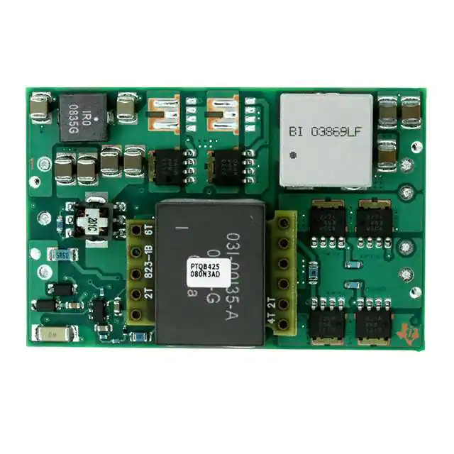
The PTQB425080 power module is single-output
isolated DC/DC converter, housed in an industry
standard quarter-brick package. The module is
nominally rated up to 200 W with a maximum load
current of 25 A. It delivers an output voltage of 1/6th
the input voltage for an input voltage range of 36 V to
55 V, while limiting the output voltage to 10.5 V for an
input voltage greater than 55 V.
The PTQB425080 operates from a standard 48-V
telecom central office (CO) supply and occupies only
3.3 in2 of PCB area. The module offers OEMs a
compact and flexible high-output power source in an
industry standard footprint. It is suitable for distributed
power applications in both telecom and computing
environments that utilize an intermediate bus
architecture (IBA), and may be used for powering
downstream point-of-load (POL) devices such as the
second generation PTH series of products (T2).
Features include a remote On/Off control with
optional logic polarity, and an undervoltage lockout
(UVLO). Protection features include output overcurrent protection (OCP) and over-temperature
protection (OTP). To compliment T2-POL products,
optional features include a SmartSync compatible
clock drive and a AutoTrack™ power-up sequencing
manager
The module is fully integrated for stand-alone
operation, and require no additional components.
STANDARD APPLICATION
+VO
+VI
1
+VI
+VO
7
+
+
PTQB425080N
CI
(Optional)
−VI
3
−VI
CO
(Optional)
−VO
Remote On/Off
2
4
Point−of−Load
Power Module
Inputs
−VO
UDG−06086
1
Please be aware that an important notice concerning availability, standard warranty, and use in critical applications of
Texas Instruments semiconductor products and disclaimers thereto appears at the end of this data sheet.
PRODUCTION DATA information is current as of publication date.
Products conform to specifications per the terms of the Texas
Instruments standard warranty. Production processing does not
necessarily include testing of all parameters.
Copyright © 2006–2007, Texas Instruments Incorporated
�Not Recommended for New Designs
PTQB425080
SLTS269B – DECEMBER 2006 – REVISED NOVEMBER 2007
www.ti.com
This integrated circuit can be damaged by ESD. Texas Instruments recommends that all integrated circuits be handled with
appropriate precautions. Failure to observe proper handling and installation procedures can cause damage.
ESD damage can range from subtle performance degradation to complete device failure. Precision integrated circuits may be more
susceptible to damage because very small parametric changes could cause the device not to meet its published specifications.
ORDERING INFORMATION
For the most current package and ordering information, see the Package Option Addendum at the end of this datasheet, or see the TI
website at www.ti.com.
Table 1. PART NUMBERING SCHEME
Input
Voltage
PTQB
Output
Current
4
4 = 48 V
Output Voltage
25
25 = 25A
Enable
080
Electrical Options
N
080 = 8 V
2
Pin Style
A
N = Negative
2 = Standard
P = Positive
3 = SmartSync
Clock Drive and
AutoTrack™ Enable
D
D = Through-hole, Pb-free
ABSOLUTE MAXIMUM RATING
UNIT
TA
VI,
MAX
PO,
Operating Temperature
Range
Maximum Input Voltage
Maximum Output Power
–40°C to 85°C (1)
Over VI Range
Continuous voltage
75 V
Peak voltage for 100 ms duration
100 V
VI = 48 V
200 W
MAX
TS
Storage Temperature
–40°C to 125°C
Mechanical Shock
Per Mil-STD-883, Method 2002.3 1 ms, 1/2
Sine, mounted
AD Suffix
250 G
Mechanical Vibrarion
Per Mil-STD-883, Method 2007.2 20-2000 Hz,
PCB mounted
AD Suffix
15 G
Weight
Flammability
(1)
2
30 grams
Meets UL 94V-O
See SOA curves or consult factory for appropriate derating.
Submit Documentation Feedback
Copyright © 2006–2007, Texas Instruments Incorporated
Product Folder Links: PTQB425080
�Not Recommended for New Designs
PTQB425080
www.ti.com
SLTS269B – DECEMBER 2006 – REVISED NOVEMBER 2007
ELECTRICAL CHARACTERISTICS PTQB425080
(Unless otherwise stated, TA = 25°C, VI = 48 V, VO = 8 V, CO = 10 μF, and IO = IOmax
PARAMETER
TEST CONDITIONS
MIN
IO
Output Current
Over VI range
0
VI
Input Voltage Range
Over IO range
36
VO tol
Output Voltage Tolerance
Over VI and IO range
5.4
36 ≤ VI ≤ 55 V
TYP
48
MAX
UNIT
25
A
75
V
10.5
0.17
V
V/V
Regline
Line Regulation
55 < VI ≤ 75 V, VO = 9.5 V
10
%
Regload
Load Regulation
Over IO range
40
mV/A
η
Efficiency
IO = IOmax
VR
VO Ripple (pk-pk)
20 MHz bandwidth
ITRIP
Overcurrent Threshold
Shutdown, followed by auto-recovery
OTP
Over Temperature
Protection
Temperature Measurement at thermal sensor. Hysteresis =
10°C nominal.
fs
Switching Frequency
Over VI range
UVLO
Undervoltage Lockout
93%
100
mVpp
35
A
125
°C
275
kHz
VOFF
VI decreasing, IO = 10 A
32.5
VHYS
Hysteresis
1.5
V
On/Off Input: Negative Enable
VIH
Input High Voltage
VIL
Input Low Voltage
IIL
Input Low Current
Referenced to –VI
2.4
Open (1)
–0.2
0.8
–0.3
V
mA
On/Off Input: Positive Enable
4.5
Open (1)
–0.2
0.8
VIH
Input High Voltage
VIL
Input Low Voltage
IIL
Input Low Current
IISB
Standby Input Current
Output disabled (pin 2 status set to Off)
CI
External Input Capacitance
Between +VI and –VI
0
CO
External Output
Capacitance
Between +VO and –VO
0
Isolation Voltage
Input-to-output and input-to-case
Isolation Capacitance
Input-to-output
Isolation Resistance
Input-to-output
SmartSync Clock Drive
(pin 5)
TTL Output signal for
synchronizing POL modules
fss
(1)
Referenced to –VI
V
–0.5
mA
3
mA
100
μF
3000
1500
μF
Vdc
500
10
pF
MΩ
Signal Amplitude
5
Signal Frequency
275
Vpk-pk
kHz
The Remote On/Off input has an internal pull-up and may be controlled with an open collector (drain) interface. An open circuit
correlates to a logic high. Consult the application notes for interface considerations.
Submit Documentation Feedback
Copyright © 2006–2007, Texas Instruments Incorporated
Product Folder Links: PTQB425080
3
�Not Recommended for New Designs
PTQB425080
SLTS269B – DECEMBER 2006 – REVISED NOVEMBER 2007
www.ti.com
TERMINAL FUNCTIONS
TERMINAL
NAME
DESCRIPTION
NO.
+VI
(1)
1
The positive input for the module with respect to -VI. When powering the module from a negative input voltage,
this input is connected to the input source ground.
–VI
(1)
3
The negative input supply for the module, and the 0-V reference for the enable input. When powering the module
from a positive source, this input is connected to the input source return.
Remote On/Off
2
This input controls the On/Off status of the output voltage. It is either driven low (–VI potential), or left open-circuit.
For units identified with the N (negative logic) option, applying a logic low to this pin enables the output. And for
units identified with the P (positive logic) option, the output is disabled.
+VO
7
This is the positive power output with respect to –VO. It is isolated from the input power pins and produces a valid
output voltage approximately 80 ms before the voltage at the Track terminal is allowed to rise. This provides the
required standby power source to any downstream nonisolated modules in power-up sequencing applications.
–VO
4
This is the output power return for both the +VO output voltage. This terminal should be connected to the common
of the load circuit.
AutoTrack™
Enable
(Optional)
6
This terminal may be used in power-up sequencing applications to control the output voltage of Auto-Track
compatible modules, powered from the converter +VO output. The converter Track control has an internal, opencollector transistor, which holds the voltage close to –VO potential for approximately 80 ms after the +VO output is
in regulation. Following this delay, the Track voltage rises simultaneously with the output voltages of all other
modules controlled by Auto-Track. See Application Information for more details.
SmartSync
Clock Drive
(Optional)
5
This terminal sources a 275kHz clock signal that can be used to synchronize the switching frequency of multiple
downstream point-of-load power modules. Frequency synchronization eliminates beat frequencies and reduces
the external filtering requirement. See Application Information for more details.
(1)
These functions indicate signals electrically common with the input.
spacer
PTQB425080x3
1
2
3
4
+VO
Track
+VI
7
6
1
2
On/Off
−VI
PTQB425080x2
SmartSync
−VO
5
4
3
Submit Documentation Feedback
+VI
+VO
7
On/Off
−VI
−VO
4
Copyright © 2006–2007, Texas Instruments Incorporated
Product Folder Links: PTQB425080
�Not Recommended for New Designs
PTQB425080
www.ti.com
SLTS269B – DECEMBER 2006 – REVISED NOVEMBER 2007
TYPICAL CHARACTERISTICS
PTQB425080
(1) (2)
EFFICIENCY
vs
LOAD CURRENT
POWER DISSIPATION
vs
LOAD CURRENT
AMBIENT TEMPERATURE
vs
LOAD CURRENT
90
20
100
VI = 48 V
600 LFM
VI = 75 V
18
95
80
h - Efficiency - %
90
85
VI = 75 V
VI = 36 V
80
75
VI
70
VI = 48 V
14
12
10
8
6
VI
4
36 V
48 V
75 V
65
36 V
48 V
75 V
2
5
10
15
IO - Output Current - A
20
5
0
25
100 LFM
60
Natural
Convection
50
VI = 48 V
LFM
40
0
100
200
400
600
400 LFM
20
10
15
20
IO - Output Current - A
Figure 1.
200 LFM
70
30
VI = 36 V
0
60
0
TA - Ambient Temperature - °C
PD - Power Dissipation - W
16
25
0
5
10
15
20
IO - Output Current - A
Figure 2.
25
Figure 3.
LINE REGULATION
LOAD REGULATION
12
12
IO = 12 A
VI = 60 V
VI = 75 V
10
10
VO - Output Voltage - V
VO - Output Voltage - V
IO = 0 A
8
6
IO = 25 A
4
8
6
4
VI = 36 V
IO
0
36
36 V
48 V
60 V
75 V
0
42
48
54
60
66
72
78
0
VI – Input Voltage – V
(2)
5
10
15
20
25
IO - Output Current - A
Figure 4.
(1)
VI
2
0A
12 A
25 A
2
VI = 48 V
Figure 5.
All data listed in Figure 1, Figure 2, Figure 4, and Figure 5 have been developed from actual products tested at 25°C. This data is
considered typical data for the dc-dc converter.
The temperature derating curves represent operating conditions at which internal components are at or below manufacturer's maximum
rated operating temperature. Derating limits apply to modules soldered directly to a 100–mm × 100–mm, double-sided PCB with 2 oz.
copper. For surface mount packages, multiple vias (plated through holes) are required to add thermal paths around the power pins.
Please refer to the mechanical specification for more information. Applies to Figure 3.
Submit Documentation Feedback
Copyright © 2006–2007, Texas Instruments Incorporated
Product Folder Links: PTQB425080
5
�Not Recommended for New Designs
PTQB425080
SLTS269B – DECEMBER 2006 – REVISED NOVEMBER 2007
www.ti.com
APPLICATION INFORMATION
Operating Features and System Considerations for the PTQB425080 Series of DC/DC
Converters
Overcurrent Protection
To protect against load faults, these converters incorporate output overcurrent protection. Applying a load to the
output that exceeds the converter's overcurrent threshold (see applicable specification) causes the output voltage
to momentarily fold back, and then shut down. Following shutdown the module periodically attempts to
automatically recover by initiating a soft-start power-up. This is often described as a hiccup mode of operation,
whereby the module continues in the cycle of successive shutdown and power up until the load fault is removed.
Once the fault is removed, the converter automatically recovers and returns to normal operation.
Overtemperature Protection
Overtemperature protection is provided by an internal temperature sensor, which closely monitors the
temperature of the converter’s printed circuit board (PCB). If the sensor exceeds a temperature of approximately
125°C, the converter shuts down. The converter then automatically restarts when the sensed temperature drops
back to approximately 95°C. When operated outside its recommended thermal derating envelope (see data sheet
SOA curves), the converter typcially cycles on and off at intervals from a few seconds to one or two minutes.
This is to ensure that the internal components are not permanently damaged from excessive thermal stress.
Undervoltage Lockout
The Undervoltage lockout (UVLO) is designed to prevent the operation of the converter until the input voltage is
at the minimum input voltage. This prevents high start-up current during normal power-up of the converter, and
minimizes the current drain from the input source during low input voltage conditions. The UVLO circuitry also
overrides the operation of the Remote On/Off control.
Primary-Secondary Isolation
The converter incorporates electrical isolation between the input terminals (primary) and the output terminals
(secondary). All converters are production tested to a withstand voltage of 1500 VDC. This specification complies
with UL60950 and EN60950 requirements. This allows the converter to be configured for either a positive or
negative input voltage source. The data sheet Pin Descriptions section provides guidance as to the correct
reference that must be used for the external control signals.
Input Current Limiting
The converter is not internally fused. For safety and overall system protection, the maximum input current to the
converter must be limited. Active or passive current limiting can be used. Passive current limiting can be a fast
acting fuse. A 125-V fuse, rated no more than 10 A, is recommended. Active current limiting can be implemented
with a current limited Hot-Swap controller.
Thermal Considerations
Airflow may be necessary to ensure that the module can supply the desired load current in environments with
elevated ambient temperatures. The required airflow rate may be determined from the Safe Operating Area
(SOA) thermal derating chart (see typical characteristics).
6
Submit Documentation Feedback
Copyright © 2006–2007, Texas Instruments Incorporated
Product Folder Links: PTQB425080
�Not Recommended for New Designs
PTQB425080
www.ti.com
SLTS269B – DECEMBER 2006 – REVISED NOVEMBER 2007
Using the Remote On/Off Function on the PTQB425080 Series of DC/DC Converters
For applications requiring output voltage On/Off control, the PTQB425080 series of DC/DC converters
incorporate a Remote On/Off control (pin 2). This feature can be used to switch the module off without removing
the applied input source voltage. When placed in the Off state, the standby current drawn from the input source
is typically reduced to 3 mA.
Negative Output Enable (N Option)
Models using the negative enable option, the Remote On/Off (pin 2) control must be driven to a logic low voltage
for the converter to produce an output. This is accomplished by either permanently connecting pin 2 to –VI (pin
3), or driving it low with an external control signal. Table 2 shows the input requirements of pin 2 for those
modules with the NEN option.
Table 2. On/Off Control Requirements
for Negative Enable
PARAMETER
MIN
TYP
MAX
VIH
Disable
2.4 V
20 V
VIL
Enable
–0.2 V
0.8 V
Vo/c
Open-Circuit
II
Pin 2 at –VI
9V
15 V
–0.75 mA
Positive Output Enable (P Option)
For those models with the positive enable option, leaving pin 2 open circuit, (or driving it to an equivalent logic
high voltage), enables the converter output. This allows the module to produce an output voltage whenever a
valid input source voltage is applied to +VI with respect to –VI. If a logic-low signal is then applied to pin 2 the
converter output is disabled. Table 3 gives the input requirements of pin 2 for modules with the PEN option.
Table 3. On/Off Control Requirements
for Positive Enable
PARAMETER
MIN
TYP
MAX
VIH
Enable
4.5 V
20 V
VIL
Disable
–0.2 V
0.8 V
Vo/c
Open-Circuit
II
Pin 2 at –VI
5V
7V
–0.5 mA
Notes:
1. The Remote On/Off control uses –VI (pin 3) as its ground reference. All voltages are with respect to –VI.
2. An open-collector device (preferably a discrete transistor) is recommended. A pull-up resistor is not required.
If one is added the pull-up voltage should not exceed 20 V.
Caution: Do not use a pull-resistor to +VI (pin 1). The remote On/Off control has a maximum input voltage of
20 V. Exceeding this voltage can overstress, and possibly damage, the converter.
3. The Remote On/Off pin may be controlled with devices that have a totem-pole output. This is provided the
output high level voltage (VOH) meets the module's minimum VIH specified in Table 2. If a TTL gate is used, a
pull-up resistor may be required to the logic supply voltage.
4. The converter incorporates an undervoltage lockout (UVLO). The UVLO keeps the converter off until the
input voltage is close to the minimum specified operating voltage. This is regardless of the state of the
Remote On/Off control. Consult the product specification for the UVLO input voltage thresholds.
Submit Documentation Feedback
Copyright © 2006–2007, Texas Instruments Incorporated
Product Folder Links: PTQB425080
7
�Not Recommended for New Designs
PTQB425080
SLTS269B – DECEMBER 2006 – REVISED NOVEMBER 2007
www.ti.com
PTQB425080P
2
1 = Disable
Remote On/Off
Q1
BSS138
−VI
3
−VI
UDG−06085
Figure 6. Recommended Control for Remote On/Off Input
Turn-On: With a valid input source voltage applied, the converter produces a regulated output voltage within 75
ms of the output being enabled. Figure 7 shows the output response of the PTQB425080P following the removal
of the logic-low signal from the Remote On/Off (pin 2); see Figure 6. This corresponds to the drop in Q1 VGS in
Figure 7. Although the rise-time of the output voltage is short (