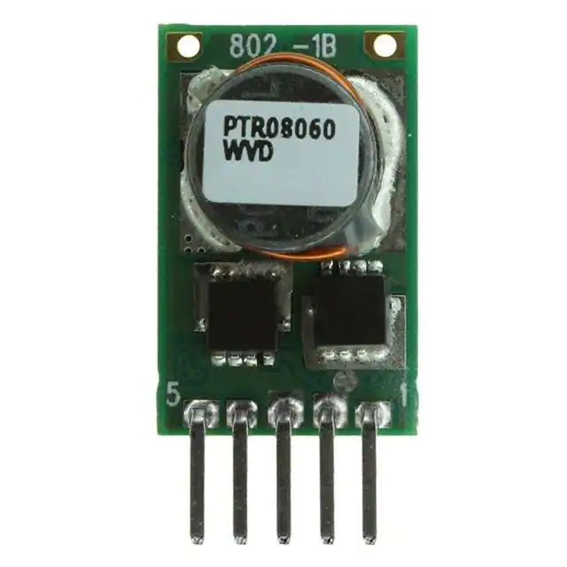
PTR08060W
www.ti.com
SLTS289G – AUGUST 2007 – REVISED MARCH 2013
6-A, 4.5-V to 14-V INPUT, NON-ISOLATED,
ADJUSTABLE WIDE-OUTPUT, SWITCHING REGULATOR
Check for Samples: PTR08060W
FEATURES
APPLICATIONS
•
•
•
•
•
•
•
1
•
•
•
•
•
•
Up to 6-A Output Current
Wide Input Voltage Range (4.5 V to 14 V)
Wide-Output Voltage Adjust
(0.6 V to 5.5 V)
Efficiencies Up To 96%
ON/OFF Inhibit
Undervoltage Lockout (UVLO)
Output Overcurrent Protection
(Nonlatching, Auto-Reset)
Ambient Temp. Range: –40°C to 85°C
Space Saving Vertical SIP Package
Instrumentation
Consumer Electronics
Servers
General-Purpose Circuits
DESCRIPTION
The PTR08060W is a highly integrated, low-cost switching regulator module that delivers up to 6 A of output
current. Occupying approximate PCB area of a standard TO-220 linear regulator IC, the PTR08060W provides
output current at a much higher efficiency and with much less power dissipation, thereby eliminating the need for
a heat sink. Their small size (0.65 x 0.41 in), high efficiency, and low cost makes these modules attractive for a
variety of applications.
The input voltage range of the PTR08060W is from 4.5 V to 14 V, allowing operation from either a 5-V or 12-V
input bus. Using state-of-the-art switched-mode power-conversion technology, the PTR08060W can step down to
voltages as low as 0.6 V. The output voltage can be adjusted to any voltage over the range, 0.6 V to 5.5 V, using
a single external resistor. Operating features include an undervoltage lockout (UVLO), on/off inhibit and output
overcurrent protection. Target applications include servers, test and measurement applications, and high-end
consumer products.
VI
2
VI
VO
4
VO
PTR08060W
Inhibit
1
Inhibit
CI
100 mF
(Required)
GND
GND
VOAdjust
3
5
RSET
1%, 0.05 W
CO
100 mF
(Required)
L
O
A
D
GND
UDG-07129
1
Please be aware that an important notice concerning availability, standard warranty, and use in critical applications of
Texas Instruments semiconductor products and disclaimers thereto appears at the end of this data sheet.
PRODUCTION DATA information is current as of publication date.
Products conform to specifications per the terms of the Texas
Instruments standard warranty. Production processing does not
necessarily include testing of all parameters.
Copyright © 2007–2013, Texas Instruments Incorporated
�PTR08060W
SLTS289G – AUGUST 2007 – REVISED MARCH 2013
www.ti.com
This integrated circuit can be damaged by ESD. Texas Instruments recommends that all integrated circuits be handled with
appropriate precautions. Failure to observe proper handling and installation procedures can cause damage.
ESD damage can range from subtle performance degradation to complete device failure. Precision integrated circuits may be more
susceptible to damage because very small parametric changes could cause the device not to meet its published specifications.
ORDERING INFORMATION
For the most current package and ordering information, see the Package Option Addendum at the end of this datasheet, or see
the TI website at www.ti.com.
ABSOLUTE MAXIMUM RATINGS
over operating free-air temperature range unless otherwise noted (1)
UNIT
TA
Operating free-air
temperature
Over VI range
Twave
Wave solder temperature
Surface temperature of module body or pins
(5 seconds maximum)
Tstg
Storage temperature
Storage temperature of module removed from shipping package
Tpkg
Packaging temperature
Shipping Tray storage or bake temperature
(1)
(2)
-40 to 85
260
(2)
°C
-55 to 125
45
Stresses beyond those listed under absolute maximum ratings may cause permanent damage to the device. These are stress ratings
only, and functional operation of the device at these or any other conditions beyond those indicated under recommended operating
conditions is not implied. Exposure to absolute-maximum-rated conditions for extended periods may affect device reliability.
This product is not compatible with surface-mount reflow solder processes.
RECOMMENDED OPERATING CONDITIONS
MIN
MAX
UNIT
VI
Input voltage
4.5
14
V
TA
Operating free-air temperature
–40
85
°C
PACKAGE SPECIFICATIONS
PTR08060W
UNIT
Weight
Flammability
Mechanical shock
Mechanical vibration
(1)
2
2.74 grams
Meets UL 94 V-O
Per Mil-STD-883D, Method 2002.3, 1 msec, 1/2 sine, mounted
Mil-STD-883D, Method 2007.2, 20-2000 Hz
250 G
15 G
(1)
(1)
Qualification limit.
Submit Documentation Feedback
Copyright © 2007–2013, Texas Instruments Incorporated
Product Folder Links: PTR08060W
�PTR08060W
www.ti.com
SLTS289G – AUGUST 2007 – REVISED MARCH 2013
ELECTRICAL CHARACTERISTICS
at 25°C free-air temperature, VI = 12 V, VO = 3.3 V, IO = IO(Max), CI = 100 µF, CO = 100 µF (unless otherwise noted)
PARAMETER
IO
Output current
TEST CONDITIONS
MIN
TA = 85°C, 100LFM airflow
TYP
MAX
0
0.6 V ≤ VO ≤ 3.6
4.5
3.6 V < VO ≤ 5.5
VO /0.83 (2)
6
14
UNIT
A
(1)
VI
Input voltage range
Over IO range
VO(adj)
Output voltage adjust range
Over IO range
Set-point voltage tolerance
TA = 25°C
Temperature variation
-40°C ≤ TA ≤ +85°C
±0.2
% VO
Line regulation
Over VI range
±0.3
% VO
Load regulation
Over IO range
±0.5
Total output voltage variation
Includes set-point, line, load, –40°C ≤ TA ≤ +85°C
VO
0.6
Efficiency
ILIM
92 %
(2)
95 %
TA = 25°C
VI = 5 V
IO = 5 A
RSET = 619 Ω, VO = 2.5 V
93 %
RSET = 976 Ω, VO = 1.8 V
91 %
RSET = 1.3 kΩ, VO = 1.5 V
90 %
RSET = 1.91 kΩ, VO = 1.2 V
88 %
RSET = 2.87 kΩ, VO = 1 V
86 %
RSET = 10.7 kΩ, VO = 0.7 V
84 %
50
Reset, followed by autorecovery
10
A
Recovery time
50
µs
VO
over/undershoot
150
mV
Undervoltage lockout
2.5 A/µs load step from 50 to 100% IOmax
VI = increasing
4.25
VI = decreasing
3.8
Input low voltage (VIL)
Input standby current
Pin 1 to GND
FS
Switching frequency
Over VI and IO ranges
CI
External input capacitance
Non-ceramic
External output capacitance
(4)
(5)
(6)
(7)
(8)
Calculated reliability
mVPP
4.4
3.95
open
–0.3
Input low current (IIL)
II(stby)
(1)
(2)
(3)
% VO
Overcurrent threshold
Input high voltage (VIH)
MTBF
(3)
20 MHz bandwith
Inhibit control (pin 1)
CO
V
% VO
% VO
±3
RSET = 267 Ω, VI = 12 V, VO = 5 V (2)
(3)
V
Output voltage ripple
Transient response
UVLO
5.5
±2
RSET = 432 Ω, VO = 3.3 V
η
14
100
(5)
100
(6)
Ceramic
0.6
µA
1
mA
300
kHz
µF
3000
(6)
(7)
100
(8)
5
Per Bellcore TR-332, 50% stress,
TA = 40°C, ground benign
13.7
V
–125
22
Equivalent series resistance (non-ceramic)
V
(4)
µF
mΩ
106 Hrs
For output voltages less than 1.0 V, the output ripple may increase (up to 2×) when operating at input voltages greater than (VO ×15).
The minimum input voltage is 4.5 V or (VO/0.83) V, whichever is greater.
The set-point voltage tolerance is affected by the tolerance and stability of RSET. The stated limit is unconditionally met if RSET has a
tolerance of 1% with with 100 ppm/°C or better temperature stability.
This control pin has an internal pullup to the input voltage VI. If it is left open circuit, the module operates when input power is applied.
The open pin voltage is 2.8 V (typ). A small low-leakage (