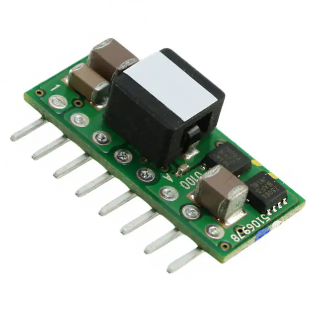
PTV03010W
www.ti.com
SLTS241A – FEBRUARY 2005 – REVISED JULY 2007
8-A, 3.3-V INPUT NONISOLATED WIDE-OUTPUT ADJUST SIP MODULE
FEATURES
APPLICATIONS
•
•
•
•
•
•
•
•
•
•
•
•
•
•
•
•
Up to 8-A Output Current
3.3-V Input Bus
Wide-Output Voltage Adjust
(0.8 V to 2.5 V)
Efficiencies up to 93%
On/Off Inhibit
Prebias Start-Up
Undervoltage Lockout
Auto-Track™ Sequencing
Output Overcurrent Protection
(Nonlatching, Auto-Reset)
Operating Temperature: –40°C to 85°C
Safety Agency Approvals:
UL/IEC/CSA-22.2 60950-1
POLA™ Compatible
Multivoltage Digital Systems
High-Density Logic Circuits
High-End Computers and Servers
3.3-V Intermediate Bus Architectures
DESCRIPTION
The PTV03010W is a ready-to-use nonisolated power module, and part of a new class of complete dc/dc
switching regulators from Texas Instruments. These regulators combine high performance with double-sided,
surface-mount construction, to give designers the flexibility to power the most complex multiprocessor digital
systems using off-the-shelf catalog parts.
The PTV03010W series is produced in a 8-pin, single in-line pin (SIP) package. The SIP footprint minimizes
board space, and offers an alternate package option for space conscious applications. Operating from a 3.3-V
input bus, the series provides step-down conversion to a wide range of output voltages, at up to 8 A of output
current. The output voltage can be set to any value over the range, 0.8 V to 2.5 V. The output voltage is set
using a single external resistor.
This series includes Auto-Track™. Auto-Track™ simplifies the task of supply-voltage sequencing in a power
system by enabling the output voltage of multiple modules to accurately track each other, or any external
voltage, during power up and power down.
Other operating features include an on/off inhibit, and the ability to start up into an existing output voltage or
prebias. A nonlatching overcurrent trip protects against load faults.
Target applications include complex multivoltage, multiprocessor systems that incorporate the industry's
high-speed microprocessors, bus drivers, and the TMS320™ DSP family.
Please be aware that an important notice concerning availability, standard warranty, and use in critical applications of Texas
Instruments semiconductor products and disclaimers thereto appears at the end of this data sheet.
POLA, Auto-Track, TMS320 are trademarks of Texas Instruments.
PRODUCTION DATA information is current as of publication date.
Products conform to specifications per the terms of the Texas
Instruments standard warranty. Production processing does not
necessarily include testing of all parameters.
Copyright © 2005–2007, Texas Instruments Incorporated
�PTV03010W
www.ti.com
SLTS241A – FEBRUARY 2005 – REVISED JULY 2007
STANDARD APPLICATION
Track
5
Track
VI
8
VI
Inhibit
GND
6
7
C1*
100 mF
(Required)
Inhibit
VO
PTV03010
VO
2, 3
VOAdj
1
4
C2*
10 mF
Ceramic
(Required)
RSET#
1%
0.05 W
(Required)
C3*
100 mF
(Optional)
C4*
10 mF
Ceramic
(Optional)
GND
L
O
A
D
GND
* See the Application Information section for capacitor recommendations.
#R
SET is required to adjust the output voltage higher than its lowest value.
See the Application Information section for values.
ORDERING INFORMATION
PTV03010 (Basic Model)
(1)
(2)
Output Voltage Range
Part Number
DESCRIPTION
Pb - free and
RoHS
Mechanical
Package (1)
0.8 V – 2.5 V (Adjustable)
PTV03010WAH
Vertical T/H
Yes (2)
EVA
See the applicable package drawing for dimensions and PC board layout.
Lead (Pb) - free specifies Sn/Ag pin solder material.
ABSOLUTE MAXIMUM RATINGS
over operating free-air temperature range unless otherwise noted (1)
UNIT
V(Track)
Track input voltage
–0.3 V to VI +0.3 V
TA
Operating temperature range
Over VI range
Lead temperature
5 seconds
–40°C to 85°C
260°C
(2)
Tstg
Storage temperature
–55°C to 125°C
V(INH)
Inhibit input voltage
–0.3 V to VI + 0.3 V
(1)
(2)
Stresses beyond those listed under absolute maximum ratings may cause permanent damage to the device. These are stress ratings
only, and functional operation of the device at these or any other conditions beyond those indicated under recommended operating
conditions is not implied. Exposure to absolute-maximum-rated conditions for extended periods may affect device reliability.
This product is not compatible with surface-mount reflow solder processes.
PACKAGE SPECIFICATIONS
PTV03010W (Suffix AH)
Weight
Meets UL 94 V-O
Mechanical shock
Per Mil-STD-883D, Method 2002.3, 1 ms, 1/2 sine, mounted
Mechanical vibration
(1)
2
2.5 grams
Flammability
Mil-STD-883D, Method 2007.2, 20 Hz - 2000 Hz
Qualification limit.
Submit Documentation Feedback
500 G
10 G
(1)
(1)
�PTV03010W
www.ti.com
SLTS241A – FEBRUARY 2005 – REVISED JULY 2007
ELECTRICAL CHARACTERISTICS
operating at 25C free-air temperature, VI = 3.3 V, VO = 2.5 V, C1 = 100 µF, C2 = 10 µF, C3 = 0 µF, and IO = IO max (unless
otherwise noted)
PARAMETER
TEST CONDITIONS
IO
Output current
Natural convection airflow
VI
Input voltage range
Over IO load range
MIN
TYP
MAX
0
2.95
η
±2
(2)
A
V
%Vo
Temperature variation
–40°C < TA < 85°C
±0.5
%Vo
Line regulation
Over VI range
±5
mV
Load regulation
Over IO range
±5
Total output variation
Includes set-point, line, load, –40°C ≤ TA ≤ 85°C
Adjust range
Over VI range
Efficiency
IO (trip)
(1)
3.65
Set-point voltage tolerance
VO
UNIT
8
0.8
IO = IO max
mV
±3
(2)
2.5
RSET = 2.21 kΩ, VO = 2.5 V
93%
RSET = 5.49 kΩ, VO = 1.8 V
90%
RSET = 8.87 kΩ, VO = 1.5 V
89%
RSET = 17.4 kΩ, VO = 1.2 V
87%
RSET = 36.5 kΩ, VO = 1 V
85%
%Vo
V
Output voltage ripple
(pk-pk)
20-MHz bandwidth
20
mVPP
Overcurrent threshold
Reset, followed by auto-recovery
16
A
1-A/s load step, 50 to 100% IO max, C3 = 100 µF
Transient response
Track control (pin 5)
UVLO
Undervoltage lockout
70
µs
100
mV
IIL Input low current
Pin to GND
Control slew-rate limit
C3 ≤ C3 (max)
1
2.45
VI decreasing
2.2
VIL Input low voltage
IIL Input low current
Inhibit (pin 7) to GND, Track (pin 5) open
ƒS
Switching frequency
Over VI and IO ranges
–0.2
Ceramic (C2)
Capacitance value
(1)
(2)
(3)
(4)
(5)
(6)
(7)
Reliability
100
10
kHz
(4)
0
Ceramic
0
Per Telcordia SR-332, 50% stress, TA = 40°C, ground
benign
V
mA
650
µF
(4)
Nonceramic
4
600
V
mA
10
Equivalent series resistance (nonceramic)
MTBF
0.6
550
mA
V/ms
(3)
0.24
Nonceramic (C1)
External input capacitance
Open
Pin to GND
Input standby current
2.8
2.4
VI – 0.5
Referenced to GND
II (stby)
External output capacitance
(C3)
–0.13
VI increasing
VIH Input high voltage
Inhibit control (pin 7)
Recovery time
Vo over/undershoot
100 (5)
11,000
(6)
300
(7)
µF
mΩ
5
106 Hr
See thermal derating curves for safe operating area (SOA), or consult factory for appropriate derating.
The set-point voltage tolerance is affected by the tolerance and stability of RSET. The stated limit is unconditionally met if RSET has a
tolerance of 1%, with 100 ppm/°C or better temperature stability.
This control pin is internally pulled up to the input voltage, VI. If this input is left open-circuit, the module operates when input power is
applied. A small low-leakage (< 100 nA) MOSFET is recommended for control. For further information, see the related application note.
A 10-µF high-frequency ceramic capacitor and 100-µF electrolytic input capacitor are required for proper operation. The electrolytic
capacitor must be rated for 300 mArms minimum ripple current. See the Application Information for further guidance on capacitor
selection.
An external output capacitor is not required for basic operation. Adding 100 µF of distributed capacitance at the load improves the
transient response.
This is the calculated maximum. The minimum ESR limitation often results in a lower value. When controlling the Track pin using a
voltage supervisor, CO(max) is reduced to 2200 μF. See the Application Information for further guidance.
This is the typical ESR for all the electrolytic (nonceramic) output capacitance. Use 7 mΩ as the minimum when using maximum-ESR
values to calculate.
Submit Documentation Feedback
3
�PTV03010W
www.ti.com
SLTS241A – FEBRUARY 2005 – REVISED JULY 2007
TYPICAL CHARACTERISTICS (3.3-V INPUT)
(8) (9)
EFFICIENCY
vs
OUTPUT CURRENT
100
OUTPUT VOLTAGE RIPPLE
vs
OUTPUT CURRENT
60
VO- Output Ripple Voltage - mVPP
VO = 2.5 V
Efficiency - %
90
80
VO = 1.5 V
VO = 1.2 V
70
VO = 0.8 V
60
50
0
2
1
3
4
5
6
7
10
0
0
1
2
3
4
5
6
7
IO - Output Current - A
Figure 1.
Figure 2.
POWER DISSIPATION
vs
OUTPUT CURRENT
TEMPERATURE DERATING
vs
OUTPUT CURRENT
80
1.6
Temperature Derating- oC
PD - Power Dissipation - W
20
8
90
1.2
0 .8
0 .4
1
2
3
4
5
6
7
8
400 LFM
200 LFM
70
100 LFM
60
Air Flow
Nat Conv
50
40
30
20
0
Airflow is parallel to the
long axis of the module
1
2
3
4
5
6
7
8
IO - Output Current - A
IO - Output Current - A
Figure 3.
4
30
8
0
(9)
40
IO - Output Current - A
2
(8)
50
Figure 4.
The electrical characteristic data has been developed from actual products tested at 25C. This data is considered typical for the
converter. Applies to Figure 1, Figure 2, and Figure 3.
The temperature derating curves represent the conditions at which internal components are at or below the manufacturer's maximum
operating temperatures. The airflow direction is parallel to the long axis of the module. Derating limits apply to modules soldered directly
to a 100 mm x 100 mm double-sided PCB with 2 oz. copper. Applies to Figure 4.
Submit Documentation Feedback
�PTV03010W
www.ti.com
SLTS241A – FEBRUARY 2005 – REVISED JULY 2007
DEVICE INFORMATION
TERMINAL FUNCTIONS
TERMINAL
NAME
DESCRIPTION
NO.
VI
8
VO
2, 3
The regulated positive power output with respect to the GND node.
GND
1, 6
This is the common ground connection for the VI and VO power connections. It is also the 0-Vdc reference for the
control inputs.
Inhibit
7
The Inhibit pin is an open-collector/drain, active-low input that is referenced to GND. Applying a low-level ground
signal to this input disables the module output and turns off the output voltage. When the Inhibit control is active,
the input current drawn by the regulator is significantly reduced. If the inhibit feature is not used, the control pin is
left open-circuit. The module then produces an output voltage whenever a valid input source is applied.
Vo Adjust
4
The positive input voltage power node to the module, which is referenced to common GND.
A 1% resistor must be connected directly between this pin and GND (pin 1 is recommended) to set the output
voltage of the module higher than its lowest value. The temperature stability of the resistor should be 100 ppm/C
(or better). The set-point range is 0.8 V to 2.5 V. The resistor value is calculated using a formula. If this input is
left open-circuit, the output voltage defaults to its lowest value. For further information, see the related application
note.
The specification table gives the standard resistor values for a number of common output voltages.
Track
5
This is an analog control input that enables the output voltage to follow an external voltage. This pin becomes
active typically 20 ms after the input voltage has been applied, and allows direct control of the output voltage from
0 V up to the nominal set-point voltage. Within this range, the output follows the voltage at the Track pin on a
volt-for-volt basis. When the control voltage is raised above this range, the module regulates at its set-point
voltage. The feature allows the output voltage to rise simultaneously with other modules powered from the same
input bus. If unused, this input should be connected to VI.
NOTE: Due to the undervoltage lockout feature, the output of the module cannot follow its own input voltage
during power up. See the related Application Information for further guidance.
Front View of Module
PIN 1
Figure 5. Pin Terminal Locations
Submit Documentation Feedback
5
�PTV03010W
www.ti.com
SLTS241A – FEBRUARY 2005 – REVISED JULY 2007
APPLICATION INFORMATION
Capacitor Recommendations for the PTV03010W Power Module
Input Capacitors
The required input capacitors are a 10-µF ceramic and a minimum of 100-µF electrolytic type. The 100-µF
capacitance must be rated for 300 mArms ripple current capability. See Table 1.
The above ripple current requirements are conditional that the 10-µF ceramic capacitor is present. The 10-µF
X5R/X7R ceramic capacitor is necessary to reduce both the magnitude of ripple current through the electroytic
capacitor and the amount of ripple current reflected back to the input source. Ceramic capacitors should be
located within 0.5 inch. (1,3 cm) of the module's input pins. Additional ceramic capacitors can be added to
reduce the RMS ripple current requirement for the electrolytic capacitor.
Ripple current (rms) rating, less than 150-mΩ equivalent series resistance (ESR), and temperature are the major
considerations when selecting input capacitors. Unlike polymer-tantalum capacitors, regular tantalum capacitors
have a recommended minimum voltage rating of 2 × (max. dc voltage + ac ripple). This is standard practice to
ensure reliability. Only a few tantalum capacitors were found to have sufficient voltage rating to meet this
requirement. At temperatures below 0°C, the ESR of aluminum electrolytic capacitors increases. For these
applications, Os-Con, polymer-tantalum, and polymer-aluminum types should be considered.
Output Capacitor (Optional)
For applications with load transients (sudden changes in load current), regulator response benefits from external
output capacitance. The recommended output capacitance of 100 µF allows the module to meet its transient
response specification. For most applications, a high-quality computer-grade aluminum electrolytic capacitor is
adequate. These capacitors provide decoupling over the frequency range, 2 kHz to 150 kHz, and are suitable
when ambient temperatures are above 0°C. For operation below 0°C, tantalum-, ceramic-, or Os-Con-type
capacitors are recommended. When using one or more nonceramic capacitors, the calculated ESR should be no
lower than 4 mΩ (7 mΩ using the manufacturer's maximum ESR for a single capacitor). A list of preferred
low-ESR-type capacitors are identified in Table 1.
Ceramic Capacitors
Above 150 kHz, the performance of aluminum electrolytic capacitors is less effective. Multilayer ceramic
capacitors have low ESR and a resonant frequency higher than the bandwidth of the regulator. They can be
used to reduce the reflected ripple current at the input as well as improve the transient response of the output.
When used on the output, their combined ESR is not critical as long as the total value of ceramic capacitance
does not exceed approximately 300 µF. Also, to prevent the formation of local resonances, do not place more
than five identical ceramic capacitors in parallel with values of 10 µF or greater.
Tantalum Capacitors
Tantalum-type capacitors can only be used on the output bus, and are recommended for applications where the
ambient operating temperature can be less than 0°C. The AVX TPS, Sprague 593D/594/595, and Kemet
T495/T510 capacitor series are suggested over many other tantalum types due to their higher rated surge,
power dissipation, and ripple current capability. As a caution, many general-purpose tantalum capacitors have
considerably higher ESR, reduced power dissipation, and lower ripple current capability. These capacitors are
also less reliable as they have reduced power dissipation and surge current ratings. Tantalum capacitors that
have no stated ESR or surge current rating are not recommended for power applications.
Capacitor Table
Table 1 identifies the characteristics of capacitors from a number of vendors with acceptable ESR and ripple
current (rms) ratings. The recommended number of capacitors required at both the input and output buses is
identified for each capacitor type.
Note:This is not an extensive capacitor list. Capacitors from other vendors are available with comparable
specifications. Those listed are for guidance. The RMS ripple current rating and ESR (at 100 kHz) are critical
parameters necessary to ensure both optimum regulator performance and long capacitor life.
6
Submit Documentation Feedback
�PTV03010W
www.ti.com
SLTS241A – FEBRUARY 2005 – REVISED JULY 2007
APPLICATION INFORMATION (continued)
Table 1. Input/Output Capacitors (1)
Capacitor Characteristics
Quantity
Working
Voltage
(V)
Value
(µF)
Max ESR
at 100 kHz
(Ω)
Max Ripple
Current at
85°C (Irms)
(mA)
Panasonic, Aluminum
10
330
0.117
555
8 × 11,5
1
1
EEUFC1A331
FC (Radial)
16
220
0.117
555
8 × 11,5
1
1
EEUFC1C221
FK (SMD)
6.3
470
0.16
600
8 × 10,2
1
1
EEVFK0J471P
PSA,Poly-Alum (Radial)
6.3
220
0.02
3160
6,3 × 9,8
1
≤3
LXZ, Aluminum (Radial)
10
470
0.12
555
8 × 125
1
1
LXZ10VB471M8X12LL
MVZ, Auminum (SMD)
16
680
0.09
670
10 × 10
1
1
MVZ16VC681MJ10TP
PXA, Poly-Alum (SMD)
10
120
0.027
2800
8 × 6,7
1
≤3
PXA10VC121MH70TP
Nichicon, Aluminum
16
270
0.09
575
10 × 12,5
1
1
UPM1C271MHH6
HD (Radial)
10
470
0.072
760
8 × 11,5
1
1
UHD1A471MPR
TP, Poscap
10
220
0.025
2400
7,3 × 4,3
1
≤2
10TPE220M
SEQP, Os-Con (Radial)
10
120
0.035
2500
8×7
1
≤5
10SEQP120M
SVP, Os-Con (SMD)
6.3
100
0.04
1810
6,3 × 6
1
≤3
6SVP100M
AVX, Tantalum, (SMD)
10
100
0.075
>1090
7,3 × 5,7 × 4,1
1
≤4
TPSC107M010R0075
TPS (SMD)
10
150
0.05
>1559
7,3 × 5,7 × 4,1
1
≤4
TPSD157M010R0050
T520, Poly-Tant (SMD)
10
100
0.055
1500
4,3 × 7,3 × 4
1
≤4
T520D107M010ASE055
T530, Poly-Tant/Organic
10
330
0.01
>5200
4,3 × 7,3 × 4
1
≤1
T530X337M010ASE010
94SVP, Os-Con (SMD)
10
120
0.04
2120
8×7
1
≤3
94SVP127X0010E7
595D, Tantalum (SMD)
10
220
0.14
1040
7,5 × 4,3 × 4,1
1
≤4
595D227X0010D2T
94SA, Os-Con (Radial)
10
100
0.03
2670
10 × 10,5
1
≤3
94SA107X0010EBP
Kemet, Ceramic
16
10
0.002
—
3225
≥1
(2)
≤5
C1210C106M4PAC
(2)
Capacitor Vendor,
Type, Series (Style)
Physical Size
(mm)
Input
Bus
Optional
Output
Bus
Vendor
Part Number
United Chemi-Con
PSA6.3VB220MF11
Sanyo
Kemet (SMD)
Vishay-Sprague
6.3
22
0.002
3225
≥1
≤5
C1210C226K9PAC
6.3
47
0.002
3225
≥1 (2)
≤5
C1210C476K9PAC
Murata, Ceramic
6.3
100
0.002
3225
≥1 (2)
≤3
GRM32ER60J107M
X5R (SMD)
6.3
47
≥1 (2)
≤5
GRM32ER60J476M
16
22
≥1
(2)
≤5
GRM32ER61C226K
16
10
≥1
(2)
≤5
GRM32DR61C106K
TDK, Ceramic
6.3
100
≥1 (2)
≤3
C3225X5R0J107MT
X5R (SMD)
6.3
47
≥1
(2)
≤5
C3225X5R0J476MT
16
22
≥1
(2)
≤5
C3225X5R1C226MT
16
10
≥1
(2)
≤5
C3225X5R1C106MT
X5R (SMD)
(1)
(2)
0.002
—
—
3225
Capacitor Supplier Verification
Please verify availability of capacitors identified in this table. Capacitor suppliers may recommend alternative part numbers because of
limited availability or obsolete products. In some instances, the capacitor product life cycle may be in decline and have short-term
consideration for obsolescence.
RoHS, Lead-free and Material Details
Please consult capacitor suppliers regarding material composition, RoHS status, lead-free status, and manufacturing process
requirements. Component designators or part number deviations can occur when material composition or soldering requirements are
updated.
Ceramic capacitors are required to complement electrolytic types at the input and to reduce high-frequency ripple current.
Submit Documentation Feedback
7
�PTV03010W
www.ti.com
SLTS241A – FEBRUARY 2005 – REVISED JULY 2007
Designing for Fast Load Transients
The transient response of the dc/dc converter has been characterized using a load transient with a di/dt of
1 A/µs. The typical voltage deviation for this load transient is given in the data sheet specification table using the
optional value of output capacitance. As the di/dt of a transient is increased, the response of a converter
regulation circuit ultimately depends on its output capacitor decoupling network. This is an inherent limitation
with any dc/dc converter once the speed of the transient exceeds its bandwidth capability. If the target
application specifies a higher di/dt or lower voltage deviation, the requirement can only be met with additional
output capacitor decoupling. In these cases, special attention must be paid to the type, value, and ESR of the
capacitors selected.
If the transient performance requirements exceed that specified in the data sheet, or the total amount of load
capacitance is above 3000 µF, the selection of output capacitors becomes more important.
Adjusting the Output Voltage
The VO Adjust control (pin 4) sets the output voltage of the PTV03010W product to a value over the range, 0.8 V
to 2.5 V. The adjustment method requires the addition of a single external resistor, RSET, that must be connected
directly between the VO Adjust and the regulator's output GND (pin 1 is recommended). Without an adjust
resistor, the output voltage is set to its lowest value. Table 2 gives the preferred value of the external resistor for
a number of standard voltages, along with the actual output voltage that this resistance value provides. Figure 6
shows the placement of the required resistor.
Table 2. Nearest Standard Values of RSET for Common Output Voltages
VO
(Required)
RSET
(Standard Value)
VO
(Actual)
2.5 V
2.21 kΩ
2.502 V
2V
4.12 kΩ
2.010 V
1.8 V
5.49 kΩ
1.803 V
1.5 V
8.87 kΩ
1.504 V
1.2 V
17.4 kΩ
1.202 V
1V
36.5 kΩ
1.005 V
0.8 V
Open
0.800 V
For other output voltages, the value of the required resistor can either be calculated or simply selected from the
range of values given in Table 3. Equation 1 may be used for calculating the adjust resistor value.
0.8 V
R SET + 10 kW
* 2.49 kW
V O * 0.8 V
(1)
VOAdj
GND
CO
+
GND
VO
VO
PTV03010W
RSET, 1%
GND
Figure 6. VO Adjust Resistor Placement
8
Submit Documentation Feedback
�PTV03010W
www.ti.com
SLTS241A – FEBRUARY 2005 – REVISED JULY 2007
Table 3. Calculated Values of RSET for Other Output Voltages
VO
RSET
VO
RSET
0.800
Open
1.450
9.82 kΩ
0.825
318 kΩ
1.500
8.94 kΩ
0.850
158 kΩ
1.550
8.18 kΩ
0.875
104 kΩ
1.600
7.51 kΩ
0.900
77.5 kΩ
1.650
6.92 kΩ
0.925
61.5 kΩ
1.700
6.40 kΩ
0.950
50.8 kΩ
1.750
5.93 kΩ
0.975
43.2 kΩ
1.800
5.51 kΩ
1.000
37.5 kΩ
1.850
5.13 kΩ
1.025
33.1 kΩ
1.900
4.78 kΩ
1.050
29.5 kΩ
1.950
4.47 kΩ
1.075
26.6 kΩ
2.000
4.18 kΩ
1.100
24.2 kΩ
2.050
3.91 kΩ
1.125
22.1 kΩ
2.100
3.66 kΩ
1.150
20.4 kΩ
2.150
3.44 kΩ
1.175
18.8 kΩ
2.200
3.22 kΩ
1.200
17.5 kΩ
2.250
3.03 kΩ
1.225
16.3 kΩ
2.300
2.84 kΩ
1.250
15.3 kΩ
2.350
2.67 kΩ
1.300
13.5 kΩ
2.400
2.51 kΩ
1.350
12.1 kΩ
2.450
2.36 kΩ
1.400
10.8 kΩ
2.500
2.22 kΩ
Features of the PTH/PTV Family of Nonisolated, Wide-Output Adjustable Power Modules
POLA™ Compatibility
The PTH/PTV family of nonisolated, wide-output adjustable power modules from Texas Instruments are
optimized for applications that require a flexible, high-performance module that is small in size. Each of these
products are POLA™ compatible. POLA-compatible products are produced by a number of manufacturers, and
offer customers advanced, nonisolated modules with the same footprint and form factor. POLA parts are also
ensured to be interoperable, which provides customers with a second-source option.
Submit Documentation Feedback
9
�PTV03010W
www.ti.com
SLTS241A – FEBRUARY 2005 – REVISED JULY 2007
Soft-Start Power Up
The Auto-Track feature allows the power up of multiple PTH/PTV modules to be directly controlled from the
Track pin. However, in a stand-alone configuration, or when the Auto-Track feature is not being used, the Track
pin is directly connected to the input voltage, VI (see Figure 7).
Track
3.3 V
1.8 V
GND
Adjust
RSET
C2
10 mF
5.49 kW
1%, 0.05 W
+
GND
C1
100 mF
VO
PTV03010W
VI
C3
100 mF
+
GND
L
O
A
D
GND
Figure 7. Power-Up Application Circuit
When the Track pin is connected to the input voltage, the Auto-Track function is permanently disengaged. This
allows the module to power up entirely under the control of its internal soft-start circuitry. When power up is
under soft-start control, the output voltage rises to the set-point at a quicker and more linear rate.
VI (2 V/div)
VO (1 V/div)
II (5 A/div)
t -Time = 5 ms/div
Figure 8. Power-Up Waveform
From the moment a valid input voltage is applied, the soft-start control introduces a short time delay (typically
8 ms to 15 ms) before allowing the output voltage to rise. The output then progressively rises to the module
set-point voltage. Figure 8 shows the soft-start power-up characteristic of the PTV03010W, operating from a
3.3-V input bus and configured for a 1.8-V output. The waveforms were measured with a 5-A resistive load and
the Auto-Track feature disabled. The initial rise in input current when the input voltage first starts to rise is the
charge current drawn by the input capacitors. Power up is complete within 25 ms.
10
Submit Documentation Feedback
�PTV03010W
www.ti.com
SLTS241A – FEBRUARY 2005 – REVISED JULY 2007
Output On/Off Inhibit
For applications requiring output voltage on/off control, the modules incorporate an output Inhibit control. The
inhibit feature can be used wherever there is a requirement for the output voltage from the regulator to be turned
off.
The power modules function normally when the Inhibit input is left open-circuit, providing a regulated output
whenever a valid source voltage is connected to VI with respect to GND.
Figure 9 shows the typical application of the inhibit function. Note the discrete transistor (Q1). The Inhibit input
has its own internal pullup (see footnotes to electrical characteristics table). The input is not compatible with TTL
logic devices. An open-collector (or open-drain) discrete transistor is recommended for control.
Track
VI
VI
PTV03010W
Inhibit GND
C1
GND
VO
VO
VOAdj
C2
RSET
2.21 kW
Q1
BSS138
C3
L
O
A
D
1 = Inhibit
GND
GND
Figure 9. On/Off Inhibit Application Circuit
Turning Q1 on applies a low voltage to the Inhibit control and disables the output of the module. If Q1 is then
turned off, the module executes a soft-start power-up sequence. A regulated output voltage is produced within
25 ms. Figure 10 shows the typical rise in both the output voltage and input current, following the turnoff of Q1.
The turnoff of Q1 corresponds to the rise in the waveform, Q1 VDS. The waveforms were measured with a 5-A
constant current load.
VO (1 V/div)
II (5 A/div)
Q1 VDS (5 V/div)
t - Time = 5 ms/div
Figure 10. Inhibit Waveform
Submit Documentation Feedback
11
�PTV03010W
www.ti.com
SLTS241A – FEBRUARY 2005 – REVISED JULY 2007
Overcurrent Protection (OCP)
For protection against load faults, the modules incorporate output overcurrent protection. Applying a load that
exceeds the overcurrent threshold causes the regulated output to shut down. Following shutdown, a module
periodically attempts to recover by initiating a soft-start power up. This is described as a hiccup mode of
operation, whereby the module continues in the cycle of successive shutdown and power up until the load fault
is removed. During this period, the average current flowing into the fault is significantly reduced. Once the fault is
removed, the module automatically recovers and returns to normal operation.
Auto-Track™ Function
The Auto-Track function is unique to the PTH/PTV family, and is available with all POLA products. Auto-Track
was designed to simplify the amount of circuitry required to make the output voltage from each module power up
and power down in sequence. The sequencing of two or more supply voltages during power up is a common
requirement for complex mixed-signal applications that use dual-voltage VLSI ICs such as the TMS320™ DSP
family, microprocessors, and ASICs.
How Auto-Track™ Works
Auto-Track works by forcing the module output voltage to follow a voltage presented at the Track control pin (1).
This control range is limited to between 0 V and the module set-point voltage. Once the track-pin voltage is
raised above the set-point voltage, the module output remains at its set-point (2). As an example, if the Track pin
of a 2.5-V regulator is at 1 V, the regulated output is 1 V. If the voltage at the Track pin rises to 3 V, the
regulated output does not go higher than 2.5 V.
Under Auto-Track control, the regulated output from the module follows the voltage at its Track pin on a
volt-for-volt basis. By connecting the Track pin of a number of these modules together, the output voltages follow
a common signal during power up and power down. The control signal can be an externally generated master
ramp waveform, or the output voltage from another power supply circuit (3). For convenience, the Track input
incorporates an internal RC-charge circuit. This operates off the module input voltage to produce a suitable
rising waveform at power up.
Typical Application
The basic implementation of Auto-Track allows for simultaneous voltage sequencing of a number of Auto-Track
compliant modules. Connecting the Track inputs of two or more modules forces their track input to follow the
same collective RC-ramp waveform, and allows their power-up sequence to be coordinated from a common
track control signal. This can be an open-collector (or open drain) device, such as a power-up reset voltage
supervisor IC. See U3 in Figure 11.
To coordinate a power-up sequence, the Track control must first be pulled to ground potential. This should be
done at or before input power is applied to the modules. The ground signal should be maintained for at least
20 ms after input power has been applied. This brief period gives the modules time to complete their internal
soft-start initialization (4), enabling them to produce an output voltage. A low-cost supply voltage supervisor IC,
that includes a built-in time delay, is an ideal component for automatically controlling the track inputs at power
up.
Figure 11 shows how the TPS3808G33 supply voltage supervisor IC (U3) can be used to coordinate the
sequenced power-up of two 3.3-V input Auto-Track modules. The output of the TPS3808G33 supervisor
becomes active above an input voltage of 0.8 V, enabling it to assert a ground signal to the common track
control well before the input voltage has reached the module's undervoltage lockout threshold. The ground
signal is maintained until approximately 27 ms after the input voltage has risen above U3's voltage threshold,
which is 3.07 V. The 27-ms time period is controlled by the capacitor C3. The value of 4700 pF provides
sufficient time delay for the modules to complete their internal soft-start initialization. The output voltage of each
module remains at zero until the track control voltage is allowed to rise. When U3 removes the ground signal,
the track control voltage automatically rises. This causes the output voltage of each module to rise
simultaneously with the other modules, until each reaches its respective set-point voltage.
Figure 12 shows the output voltage waveforms from the circuit of Figure 11 after input voltage is applied to the
circuit. The waveforms, VO1 and VO2 represent the output voltages from the two power modules, U1 (2.5 V) and
U2 (1.2 V), respectively. VTRK, VO1, and VO2 are shown rising together to produce the desired simultaneous
power-up characteristic.
12
Submit Documentation Feedback
�PTV03010W
www.ti.com
SLTS241A – FEBRUARY 2005 – REVISED JULY 2007
The same circuit also provides a power-down sequence. When the input voltage falls below U3's voltage
threshold, the ground signal is reapplied to the common track control. This pulls the track inputs to zero volts,
forcing the output of each module to follow, as shown in Figure 13. In order for a simultaneous power-down to
occur, the track inputs must be pulled low before the input voltage has fallen below the modules' undervoltage
lockout. This is an important constraint. Once the modules recognize that a valid input voltage is no longer
present, their outputs can no longer follow the voltage applied at their track input. During a power-down
sequence, the fall in the output voltage from the modules is limited by the maximum output capacitance and the
Auto-Track slew rate. If the Track pin is pulled low at a slew rate greater than 1 V/ms, the discharge of the
output capacitors will induce large currents which could exceed the peak current rating of the module. This will
result in a reduction in the maximum allowable output capacitance as listed in the Electrical Characteristics
table. When controlling the Track pin of the PTV03010W using a voltage supervisor IC, the slew rate is
increased, therefore COmax is reduced to 2200 μF.
Notes on Use of Auto-Track™
1. The Auto-Track function tracks almost any voltage ramp during power up, and is compatible with ramp
speeds of up to 1 V/ms.
2. The Track pin voltage must be allowed to rise above the module set-point voltage before the module
regulates at its adjusted set-point voltage.
3. The absolute maximum voltage that may be applied to the Track pin is the input voltage VI.
4. The module cannot follow a voltage at its track control input until it has completed its soft-start
initialization. This takes about 20 ms from the time that a valid voltage has been applied to its input.
During this period, it is recommended that the Track pin be held at ground potential.
5. The Auto-Track function is disabled by connecting the Track pin to the input voltage (VI). When
Auto-Track is disabled, the output voltage rises at a quicker and more linear rate after input power has
been applied.
Submit Documentation Feedback
13
�PTV03010W
www.ti.com
SLTS241A – FEBRUARY 2005 – REVISED JULY 2007
2
U1
Track
+3.3 V
3
VO
PTH03050W
Inhibit
GND
4
1
Adjust
5
+
+
C I1
U3
3
2.21 kΩ
5
SENSE
C4
0.1 µF
RESET
4
TPS3808G33
1
R TRK #
50 Ω
CT
10
U2
GND
C3
CO1
RSET1
6
VCC
MR
Vo1 = 2.5 V
6
VI
9
Up Dn
8
5
Track
Sense
2
4700 pF
2
VI
VO
PTH03060W
Inhibit
3
Adjust
GND
1
7
4
+
# RTRK = 100 Ω / N
N = Number of Track pins connected together
C I2
Vo2 = 1.2 V
6
RSET2
+
CO2
17.4 kΩ
Figure 11. Sequenced Power Up and Power Down Using Auto-Track
VTRK (1 V/div)
VTRK (1 V/div)
V01 (1 V/div)
V01 (1 V/div)
V02 (1 V/div)
V02 (1 V/div)
t − Time − 200 µs/div
t − Time − 20 ms/div
Figure 12. Simultaneous Power Up With Auto-Track
Control
14
Figure 13. Simultaneous Power Down With Auto-Track
Control
Submit Documentation Feedback
�PTV03010W
www.ti.com
SLTS241A – FEBRUARY 2005 – REVISED JULY 2007
Prebias Start-Up Capability
A prebias start-up condition occurs as a result of an external voltage being present at the output of a power
module prior to its output becoming active. This often occurs in complex digital systems when current from
another power source is backfed through a dual-supply logic component, such as an FPGA or ASIC. Another
path might be via clamp diodes, sometimes used as part of a dual-supply power-up sequencing arrangement. A
prebias can cause problems with power modules that incorporate synchronous rectifiers. This is because under
most operating conditions, such modules can sink as well as source output current. The PTH/PTV modules
incorporate synchronous rectifiers but do not sink current during start-up, or whenever the Inhibit pin is held low.
Start-up includes an initial delay (approximately 8–15 ms), followed by the rise of the output voltage under the
control of the module internal soft-start mechanism; see Figure 14.
Conditions for Prebias Holdoff
In order for the module to allow an output prebias voltage to exist (and not sink current), certain conditions must
be maintained. The module holds off a prebias voltage when the Inhibit pin is held low, and whenever the output
is allowed to rise under soft-start control. Power up under soft-start control occurs on the removal of the ground
signal to the Inhibit pin (with input voltage applied), or when input power is applied with Auto-Track disabled(1).
To further ensure that the regulator does not sink output current (even with a ground signal applied to its Inhibit),
the input voltage must also be greater than the applied prebias source, throughout the power-up sequence(2).
The soft-start period is complete when the output begins rising above the prebias voltage. The module then
functions as normal, and sinks current if a voltage higher than its set-point value is applied to its output.
Note: If a prebias condition is not present, the soft-start period is complete when the output voltage has risen to
either the set-point voltage, or the voltage applied at the module Track control pin, whichever is lowest, to its
output.
Demonstration Circuit
Figure 15 shows the start-up waveforms for the demonstration circuit shown in Figure 16. The initial rise in VO is
the prebias voltage, which is passed from the VCCIO to the VCORE voltage rail through the ASIC. Note that the
output current from the module (IO) is negligible until its output voltage rises above the applied prebias.
VI (1 V/div)
VI (1 V/div)
VO1 (1 V/div)
VO (1 V/div)
IO (5 A/div)
Start-up
Period
t - Time = 10 ms/div
t - Time = 10 ms/div
Figure 14. PTV03010W Start-Up
Submit Documentation Feedback
Figure 15. Prebias Start-Up Waveforms
15
�PTV03010W
www.ti.com
SLTS241A – FEBRUARY 2005 – REVISED JULY 2007
NOTES:
1. The prebias start-up feature is not compatible with Auto-Track. If the rise in the output is limited by the
voltage applied to the Track control pin, the output sinks current during the period that the track control
voltage is below that of the back-feeding source. For this reason, Auto-Track should be disabled when not
being used. This is accomplished by connecting the Track pin to the input voltage, VI. This raises the
Track pin well above the set-point voltage prior to start-up, which defeats the Auto-Track feature.
2. To further ensure that the regulator output does not sink current when power is first applied (even with a
ground signal applied to the Inhibit control input), the input voltage must always be greater than the
applied prebias source. This condition must exist throughout the power-up sequence of the power
system.
VI = 3.3 V
Track
VI
VO = 1.5 V
PTV03010W
GND GND
VO
+
Vadj
IO
VCCIO
VCORE
+
CI
RSET
8.87 kW
+
CO
ASIC
Figure 16. Application Circuit Demonstrating Prebias Start-Up
16
Submit Documentation Feedback
�PACKAGE OPTION ADDENDUM
www.ti.com
15-Mar-2022
PACKAGING INFORMATION
Orderable Device
Status
(1)
Package Type Package Pins Package
Drawing
Qty
Eco Plan
(2)
Lead finish/
Ball material
MSL Peak Temp
Op Temp (°C)
(3)
Device Marking
(4/5)
(6)
PTV03010WAH
ACTIVE
SIP MODULE
EVA
8
70
RoHS Exempt
& Green
SN
N / A for Pkg Type
-40 to 85
(1)
The marketing status values are defined as follows:
ACTIVE: Product device recommended for new designs.
LIFEBUY: TI has announced that the device will be discontinued, and a lifetime-buy period is in effect.
NRND: Not recommended for new designs. Device is in production to support existing customers, but TI does not recommend using this part in a new design.
PREVIEW: Device has been announced but is not in production. Samples may or may not be available.
OBSOLETE: TI has discontinued the production of the device.
(2)
RoHS: TI defines "RoHS" to mean semiconductor products that are compliant with the current EU RoHS requirements for all 10 RoHS substances, including the requirement that RoHS substance
do not exceed 0.1% by weight in homogeneous materials. Where designed to be soldered at high temperatures, "RoHS" products are suitable for use in specified lead-free processes. TI may
reference these types of products as "Pb-Free".
RoHS Exempt: TI defines "RoHS Exempt" to mean products that contain lead but are compliant with EU RoHS pursuant to a specific EU RoHS exemption.
Green: TI defines "Green" to mean the content of Chlorine (Cl) and Bromine (Br) based flame retardants meet JS709B low halogen requirements of