PTV12010L
PTV12010W
www.ti.com
SLTS234B – DECEMBER 2004 – REVISED FEBRUARY 2007
8-A, 12-V INPUT NONISOLATED WIDE-OUTPUT ADJUST SIP MODULE
FEATURES
APPLICATIONS
•
•
•
•
•
•
•
•
•
•
•
•
•
•
•
•
8 A Output Current
12-V Input Voltage
Wide-Output Voltage Adjust
(1.2 V to 5.5 V)/(0.8 V to 1.8 V)
Efficiencies up to 93%
On/Off Inhibit
Prebias Start Up
Undervoltage Lockout
Auto-Track™ Sequencing
Output Overcurrent Protection
(Nonlatching, Auto-Reset)
Operating Temperature: –40°C to 85°C
Safety Agency Approvals:
UL/IEC/CSA-22.2 60950-1
POLA™ Alliance Compatible
Multivoltage Digital Systems
High-End Computing
Networking
12-V Intermediate Bus Architectures
DESCRIPTION
The PTV12010 series of non-isolated power modules are part of a new class of complete dc/dc switching
regulator modules from Texas Instruments. These modules combine high performance with double-sided,
surface mount construction to give designers the flexibility to power the most complex multiprocessor digital
systems using off-the-shelf catalog parts.
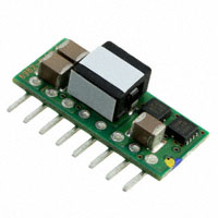
The PTV12010 series is produced in an 8-pin, single in-line pin (SIP) package. The SIP footprint minimizes
board space, and offers an alternate package option for space conscious applications. Operating from a 12-V
input bus, the series provides step-down conversion to a wide range of output voltages, at up to 8 A of output
current. The output voltage of the W-suffix parts can be set to any value over the range of 1.2 V to 5.5 V. The
L-suffix parts have an adjustment range of 0.8 V to 1.8 V. The output voltage is set using a single external
resistor.
This series includes Auto-Track™. Auto-Track™ simplifies the task of supply-voltage sequencing in a power
system by enabling the output voltage of multiple modules to accurately track each other, or any external
voltage, during power up and power down.
Other operating features include an on/off inhibit, and the ability to start up into an existing output voltage or
prebias. A nonlatching overcurrent trip and overtemperature shutdown provide protection against load faults.
Target applications include complex multivoltage, multiprocessor systems that incorporate the industry's
high-speed DSPs, microprocessors, and bus drivers.
For start-up into a non-prebiased output, review page 13 in the Application Information section.
For start-up into a prebiased output, review page 17 in the Application Information section.
Please be aware that an important notice concerning availability, standard warranty, and use in critical applications of Texas
Instruments semiconductor products and disclaimers thereto appears at the end of this data sheet.
POLA, Auto-Track, TMS320 are trademarks of Texas Instruments.
PRODUCTION DATA information is current as of publication date.
Products conform to specifications per the terms of the Texas
Instruments standard warranty. Production processing does not
necessarily include testing of all parameters.
Copyright © 2004–2007, Texas Instruments Incorporated
�PTV12010L
PTV12010W
www.ti.com
SLTS234B – DECEMBER 2004 – REVISED FEBRUARY 2007
These devices have limited built-in ESD protection. The leads should be shorted together or the device placed in conductive foam
during storage or handling to prevent electrostatic damage to the MOS gates.
STANDARD APPLICATION
Track
5
Track
VI
8
VI
PTV12010
Inhibit
C1*
100-mF
(Required)
+
C2*
10-mF
Ceramic
(Required)
6
VO
2, 3
VOAdj
GND
7
VO
1
Inhibit
4
+
RSET#
1%
0 .05 W
(Required)
C3*
100-mF
(Optional)
GND
L
O
A
D
GND
*See the application information for capacitor recommendation.
#RSET is Required to adjust the output voltage higher than its lowest value. See the application information for values.
ORDERING INFORMATION
PTV12010 (Basic Model)
(1)
Output Voltage
Part Number
DESCRIPTION
Package (1)
1.2 V – 5.5 V (Adjustable)
PTV12010WAH
Horizontal T/H
EVA
0.8 V – 1.8 V (Adjustable)
PTV12010LAH
Horizontal T/H
EVA
See the applicable package drawing for dimensions and PC board layout.
ABSOLUTE MAXIMUM RATINGS
over operating free-air temperature range unless otherwise noted (1)
UNIT
V(Track)
Track input
TA
Operating temperature range
Over VI range
Lead temperature
5 seconds
Tstg
Storage temperature
V(Inhibit)
Inhibit (pin 12) input voltage
(1)
(2)
–0.3 V to VI +0.3 V
–40°C to 85°C
260°C
(2)
–55°C to 125°C
–0.3 V to 7 V
Stresses beyond those listed under absolute maximum ratings may cause permanent damage to the device. These are stress ratings
only, and functional operation of the device at these or any other conditions beyond those indicated under recommended operating
conditions is not implied. Exposure to absolute-maximum-rated conditions for extended periods may affect device reliability.
This product is not compatible with surface-mount reflow solder processes.
PACKAGE SPECIFICATIONS
PTV12010x (Suffix AH)
Weight
Meets UL 94 V-O
Mechanical shock
Per Mil-STD-883D, Method 2002.3, 1 ms, 1/2 sine, mounted
Mechanical vibration
(1)
2
2.6 grams
Flammability
Mil-STD-883D, Method 2007.2, 20 Hz - 2000 Hz
Qualification limit.
Submit Documentation Feedback
500 Gs
15 Gs
(1)
(1)
�PTV12010L
PTV12010W
www.ti.com
SLTS234B – DECEMBER 2004 – REVISED FEBRUARY 2007
ELECTRICAL CHARACTERISTICS
operating at 25°C free-air temperature, VI = 12 V, VO = 3.3 V, C1 = 100 µF, C2 = 10 µF, C3 = 0 µF, and I O = IO max (unless
otherwise noted)
PARAMETER
PTV12010W
TEST CONDITIONS
IO
Output current
Natural convection airflow
VI
Input voltage range
Over IO load range
MIN
TYP
0
η
–40°C < TA < 85°C
Line regulation
Over VI range
±10
Load regulation
Over IO range
±12
Total output variation
Includes set-point, line, load, –40°C ≤ TA≤ 85°C
Adjust range
Over VI range
Efficiency
IO (trip)
(1)
A
V
±2%
Temperature variation
IO = IO max
UNIT
13.2
8
10.8
Set-point voltage tolerance
VO
MAX
(2)
±0.5%
mV
mV
±3
1.2
(2)
5.5
RSET = 280 Ω, VO = 5 V
92%
RSET = 2.0 kΩ, VO = 3.3 V
90%
RSET = 4.32 kΩ, VO = 2.5 V
88%
RSET = 11.5 kΩ, VO = 1.8 V
85%
RSET = 24.3 kΩ, VO = 1.5 V
83%
RSET = open cct., VO = 1.2 V
80%
%Vo
V
Output voltage ripple
(peak-to-peak)
20-MHz bandwidth
20
mVPP
Overcurrent threshold
Reset, followed by auto-recovery
16
A
1-A/µs load step, 50 to 100% IO max, C3 = 100 µF
Transient response
Track control (pin 5)
UVLO
Undervoltage lockout
IIL Input low current
70
µs
100
mV
Pin to GND
1
VI increasing
9.5
VI decreasing
VIL Input low voltage
IIL Input low current
8.8
Inhibit (pin 7) to GND, Track (pin 5) open
ƒS
Switching frequency
Over VI and IO ranges
Ceramic (C2)
Capacitance value
(1)
(2)
(3)
(4)
(5)
(6)
(7)
Reliability
100
(4)
10
(4)
Nonceramic
0
Ceramic
0
Equivalent series resistance (nonceramic)
MTBF
0.6
Per Telcordia SR-332, 50% stress, TA = 40°C, ground
benign
4
325
V
V
mA
10
250
mA
V/ms
(3)
–0.24
Nonceramic (C1)
External input capacitance
9
–0.2
Pin to GND
Input standby current
10.4
Open
Referenced to GND
II (stby)
External output capacitance (C3)
–0.13
Control slew-rate limit C3 ≤ C3 (max)
VIH Input high voltage
Inhibit control (pin 7)
Recovery time
Vo over/undershoot
mA
400
kHz
µF
100
(5)
3,300
(6)
300
µF
(7)
mΩ
5
106 Hrs
See thermal derating curves for safe operating area (SOA), or consult factory for appropriate derating.
The set-point voltage tolerance is affected by the tolerance and stability of RSET. The stated limit is unconditionally met if RSET has a
tolerance of 1%, with 100 ppm/°C or better temperature stability.
This control pin is pulled up to an internal supply voltage. To avoid risk of damage to the module, do not apply an external voltage
greater than 7 V. If this input is left open-circuit, the module operates when input power is applied. A small low-leakage (


 工商网监
湘ICP备2023018690号
工商网监
湘ICP备2023018690号
