Order
Now
Product
Folder
Support &
Community
Tools &
Software
Technical
Documents
REF3312, REF3318, REF3320, REF3325, REF3330, REF3333
SBOS392H – AUGUST 2007 – REVISED AUGUST 2019
REF33xx 3.9-μA, SC70-3, SOT-23-3, and UQFN-8, 30-ppm/°C Drift Voltage Reference
1 Features
3 Description
•
•
•
•
•
•
•
•
The REF33xx is a low-power, precision, low-dropout
voltage reference family available in tiny SC70-3 and
SOT-23-3 packages, and in a 1.5-mm × 1.5-mm
UQFN-8 package. Small size and low power
consumption (5-μA max) make the REF33xx ideal for
a wide variety of portable and battery-powered
applications.
1
Microsize Packages: SC70-3, SOT-23-3, UQFN-8
Low Supply Current: 3.9 μA (typ)
Extremely Low Dropout Voltage: 110 mV (typ)
High Output Current: ±5 mA
Low Temperature Drift: 30 ppm/°C (max)
High Initial Accuracy: ±0.15% (max)
0.1-Hz to 10-Hz Noise: 35 μVPP (REF3312)
Voltage Options: 1.2 V, 1.8 V, 2.5 V, 3 V, 3.3 V
2 Applications
•
•
•
•
•
•
•
Portable Equipment
Tablets and Smartphones
Hard Disk Drives
Sensor Modules
Data Acquisition Systems
Medical Equipment
Test Equipment
The REF33xx can be operated at a supply voltage
180 mV above the specified output voltage under
normal load conditions, with the exception of the
REF3312, which has a minimum supply voltage of
1.7 V. All models are specified for the wide
temperature range of –40°C to +125°C.
Device Information(1)
PART NUMBER
REF33xx
BODY SIZE (NOM)
SOT-23 (3)
2.92 mm × 1.30 mm
SC70 (3)
2.00 mm × 1.25 mm
UQFN (8)
1.50 mm × 1.50 mm
(1) For all available packages, see the package option addendum
at the end of the datasheet.
REF3312 in a Single-Supply Signal Chain
Dropout Voltage vs Load Current
200
+2.7V
R3
PACKAGE
R2
180
+2.7V
MSP430x20x3PW
Enable
(1)
P1.2
R1
66.5W
A0+
C1
1.5nF
VIN
OPA333,
OPA363,
or
OPA369
REF3312
VREF
C2
1mF
16-Bit
ADC
VSS
Dropout Voltage (mV)
VCC
160
+125°C
140
120
100
80
60
+25°C
40
-40°C
20
0
-5
-4
-3
-2
-1
0
1
2
3
4
5
Load Current (mA)
1
An IMPORTANT NOTICE at the end of this data sheet addresses availability, warranty, changes, use in safety-critical applications,
intellectual property matters and other important disclaimers. PRODUCTION DATA.
�REF3312, REF3318, REF3320, REF3325, REF3330, REF3333
SBOS392H – AUGUST 2007 – REVISED AUGUST 2019
www.ti.com
Table of Contents
1
2
3
4
5
6
7
Features ..................................................................
Applications ...........................................................
Description .............................................................
Revision History.....................................................
Device Comparison ...............................................
Pin Configuration and Functions .........................
Specifications.........................................................
1
1
1
2
4
4
5
7.1
7.2
7.3
7.4
7.5
7.6
5
5
5
5
6
8
Absolute Maximum Ratings ......................................
ESD Ratings..............................................................
Recommended Operating Conditions.......................
Thermal Information ..................................................
Electrical Characteristics...........................................
Typical Characteristics ..............................................
8
Parameter Measurement Information ................ 10
9
Detailed Description ............................................ 11
8.1 Thermal Hysteresis ................................................. 10
9.1 Overview ................................................................. 11
9.2 Functional Block Diagram ....................................... 11
9.3 Feature Description................................................. 11
9.4 Device Functional Modes........................................ 12
10 Applications and Implementation...................... 13
10.1 Application Information.......................................... 13
10.2 Typical Applications .............................................. 13
11 Power-Supply Recommendations ..................... 18
12 Layout................................................................... 19
12.1 Layout Guidelines ................................................. 19
12.2 Layout Example .................................................... 19
13 Device and Documentation Support ................. 20
13.1
13.2
13.3
13.4
13.5
13.6
13.7
Documentation Support ........................................
Related Links ........................................................
Receiving Notification of Documentation Updates
Community Resources..........................................
Trademarks ...........................................................
Electrostatic Discharge Caution ............................
Glossary ................................................................
20
20
20
20
20
20
20
14 Mechanical, Packaging, and Orderable
Information ........................................................... 21
4 Revision History
NOTE: Page numbers for previous revisions may differ from page numbers in the current version.
Changes from Revision G (December 2016) to Revision H
Page
•
Changed maximum operating current value in Recommended Operating Conditions section.............................................. 5
•
Changed table title to REF33xx (REF3312, REF3320, REF3325, REF3330, REF3333, REF3340) .................................... 6
Changes from Revision F (November 2016) to Revision G
•
Page
Added Long-term stability parameter and associated footnote to REF33xx section of Electrical Characteristics table ........ 6
Changes from Revision E (October 2014) to Revision F
Page
•
Changed minimum supply voltage value in second paragraph of Description section ......................................................... 1
•
Changed Device Information table ........................................................................................................................................ 1
•
Changed ESD Ratings table: changed title and format, moved Tstg parameter to Absolute Maximum Ratings table .......... 5
•
Changed supply voltage value in footnote of Recommended Operating Conditions table .................................................... 5
•
Changed supply voltage value in footnote 1 of Electrical Characteristics table .................................................................... 6
•
Changed minimum supply voltage value in Device Functional Modes section ................................................................... 12
•
Changed minimum supply voltage value in Power-Supply Recommendations section ...................................................... 18
Changes from Revision D (June 2014) to Revision E
Page
•
Added REF3325 UQFN package to data sheet ..................................................................................................................... 1
•
Added note to Applications and Implementation section...................................................................................................... 13
2
Submit Documentation Feedback
Copyright © 2007–2019, Texas Instruments Incorporated
Product Folder Links: REF3312 REF3318 REF3320 REF3325 REF3330 REF3333
�REF3312, REF3318, REF3320, REF3325, REF3330, REF3333
www.ti.com
SBOS392H – AUGUST 2007 – REVISED AUGUST 2019
Changes from Revision C (March 2014) to Revision D
Page
•
Added note to Recommended Operating Conditions............................................................................................................. 5
•
Moved Thermal Hysteresis section to Parameter Measurement Information section.......................................................... 10
•
Changed Applications and Implementation section to latest standard; added new sections .............................................. 13
Changes from Revision B (February 2014) to Revision C
•
Page
Changed Recommended Operating Conditions supply input voltage range maximum value from 55 to 5.5........................ 5
Changes from Revision A (September 2007) to Revision B
Page
•
Changed document format to meet latest data sheet standards; added new sections and moved existing sections........... 1
•
Moved package figures from front page to Pin Configuration and Functions ........................................................................ 1
•
Added new figures to front page ........................................................................................................................................... 1
•
Deleted Ordering Information table; see Package Option Addendum for most current ordering information........................ 4
•
Added RSE pin configuration ................................................................................................................................................. 4
•
Added Thermal Information table ........................................................................................................................................... 5
•
Deleted Thermal Resistance parameter in Electrical Characteristics; see new Thermal Information table........................... 7
Copyright © 2007–2019, Texas Instruments Incorporated
Submit Documentation Feedback
Product Folder Links: REF3312 REF3318 REF3320 REF3325 REF3330 REF3333
3
�REF3312, REF3318, REF3320, REF3325, REF3330, REF3333
SBOS392H – AUGUST 2007 – REVISED AUGUST 2019
www.ti.com
5 Device Comparison
PRODUCT
DESCRIPTION
REF3312
1.25 V
REF3318
1.8 V
REF3320
2.048 V
REF3325
2.5 V
REF3330
3.0 V
REF3333
3.3 V
6 Pin Configuration and Functions
REF3312, REF3318, REF3320, REF3325, REF3330, REF3333
DBZ Package and DCK Package
SOT-23-3, SC70-3
(Top View)
REF3312, REF3318, REF3320, REF3325, REF3330, REF3333
RSE Package
UQFN-8
(Top View)
OUT
IN
1
8
3
OUT
GND
NC
1
7
NC
NC
2
6
NC
NC
3
5
IN
4
2
GND
Table 1. Pin Functions
PIN
NAME
DBZ, DCK
RSE
GND
3
4
Ground
IN
1
5
Input supply voltage
NC
—
1, 2, 3, 6, 7
Not connected
OUT
2
8
Output voltage
4
Submit Documentation Feedback
DESCRIPTION
Copyright © 2007–2019, Texas Instruments Incorporated
Product Folder Links: REF3312 REF3318 REF3320 REF3325 REF3330 REF3333
�REF3312, REF3318, REF3320, REF3325, REF3330, REF3333
www.ti.com
SBOS392H – AUGUST 2007 – REVISED AUGUST 2019
7 Specifications
7.1 Absolute Maximum Ratings
over operating free-air temperature range (unless otherwise noted). (1)
MIN
Voltage
180
Operating
–50
mA
150
Junction, TJ
150
Storage, Tstg
(2)
V
5
Output short-circuit, ISC (2)
Temperature
UNIT
7.5
Output voltage
Current
(1)
MAX
Input voltage
–65
°C
150
Stresses beyond those listed under Absolute Maximum Ratings may cause permanent damage to the device. These are stress ratings
only, which do not imply functional operation of the device at these or any other conditions beyond those indicated under Recommended
Operating Conditions. Exposure to absolute-maximum-rated conditions for extended periods may affect device reliability.
See the Power-Supply Recommendations section of this data sheet.
7.2 ESD Ratings
VALUE
V(ESD)
(1)
(2)
Electrostatic discharge
Human body model (HBM), per ANSI/ESDA/JEDEC JS-001 (1)
±4000
Charged device model (CDM), per JEDEC specification JESD22-C101 (2)
±1000
Machine model (MM)
±200
UNIT
V
JEDEC document JEP155 states that 500-V HBM allows safe manufacturing with a standard ESD control process.
JEDEC document JEP157 states that 250-V CDM allows safe manufacturing with a standard ESD control process.
7.3 Recommended Operating Conditions
over operating free-air temperature range (unless otherwise noted).
MIN
VIN
Supply input voltage (1)
IOUT
Output current range
(1)
NOM
MAX
VOUT + 0.2
5.5
–5
5
UNIT
V
mA
The minimum supply voltage for the REF3312 is 1.7 V.
7.4 Thermal Information
REF3325,
REF3330
REF33xx
THERMAL METRIC
(1)
DCK (SC70)
DBZ (SOT-23)
RSE (UQFN)
UNIT
3 PINS
3 PINS
8 PINS
RθJA
Junction-to-ambient thermal resistance
279.7
313.1
61.2
°C/W
RθJC(top)
Junction-to-case (top) thermal resistance
136.3
144.0
32.6
°C/W
RθJB
Junction-to-board thermal resistance
56.9
109.3
16.0
°C/W
ψJT
Junction-to-top characterization parameter
11.0
18.2
1.3
°C/W
ψJB
Junction-to-board characterization parameter
56.1
107.9
16.0
°C/W
RθJC(bot)
Junction-to-case (bottom) thermal resistance
N/A
N/A
N/A
°C/W
(1)
For more information about traditional and new thermal metrics, see the Semiconductor and IC Package Thermal Metrics application
report.
Copyright © 2007–2019, Texas Instruments Incorporated
Submit Documentation Feedback
Product Folder Links: REF3312 REF3318 REF3320 REF3325 REF3330 REF3333
5
�REF3312, REF3318, REF3320, REF3325, REF3330, REF3333
SBOS392H – AUGUST 2007 – REVISED AUGUST 2019
www.ti.com
7.5 Electrical Characteristics
At TA = 25°C, VIN = 5 V, and ILOAD = 0 mA (unless otherwise noted).
PARAMETER
TEST CONDITIONS
MIN
TYP
MAX
UNIT
REF3312 (1.25 V)
VOUT
Output voltage
1.25
Initial accuracy
–0.15%
Output voltage noise
f = 0.1 Hz to 10 Hz
V
0.15%
35
μVPP
REF3318 (1.8 V)
VOUT
Output voltage
1.8
Initial accuracy
–0.15%
Output voltage noise
f = 0.1 Hz to 10 Hz
V
0.15%
50
μVPP
REF3320 (2.048 V)
VOUT
Output voltage
2.048
Initial accuracy
–0.15%
Output voltage noise
f = 0.1 Hz to 10 Hz
V
0.15%
55
μVPP
REF3325 (2.5 V)
VOUT
Output voltage
2.5
Initial accuracy
–0.15%
Output voltage noise
f = 0.1 Hz to 10 Hz
V
0.15%
70
μVPP
REF3330 (3.0 V)
VOUT
Output voltage
3.0
Initial accuracy
–0.15%
Output voltage noise
f = 0.1 Hz to 10 Hz
V
0.15%
84
μVPP
REF3333 (3.3 V)
VOUT
Output voltage
3.3
Initial accuracy
–0.15%
Output voltage noise
f = 0.1 Hz to 10 Hz
V
0.15%
92
μVPP
REF33xx (REF3312, REF3320, REF3325, REF3330, REF3333, REF3340)
dVOUT/dT
Output voltage temperature drift
–40°C to 85°C
9
30
–40°C to 125°C
8
30
6
50
VIN = VOUT + 200 mV to 5.5 V (1)
Line regulation
ΔVO(ΔVI)
–50
0°C to +70°C
6
–40°C to 85°C
8
–40°C to 125°C
VIN = VOUT + 200 mV (1)
Load regulation
ΔVO(ΔIL)
Long-term stability (2)
VIN – VOUT
Minimum dropout voltage (1)
6
ILOAD = ±5 mA, 0°C to 70°C
10
–40°C to 85°C
20
–40°C to 125°C
20
0h to 1000h at 25°C
55
Short-circuit current
ILOAD = ±5 mA
110
0°C to 70°C
120
–40°C to 85°C
135
–40°C to 125°C
180
(1)
(2)
(3)
6
ppm/mA
ppm
ppm
160
mV
70
Sourcing and sinking
Capacitive load
35
0.1
Turn-on settling time
50
90
ILOAD = ±2 mA, –40°C to 85°C
ISC
ppm/V
30
–50
Thermal hysteresis (3)
dT
ppm/°C
To 0.1% with CL = 1 μF
mA
10
2
μF
ms
The minimum supply voltage for the REF3312 is 1.7 V.
The long-term stability number reduces as the time increases.
The thermal hysteresis procedure is explained in more detail in the Thermal Hysteresis section.
Submit Documentation Feedback
Copyright © 2007–2019, Texas Instruments Incorporated
Product Folder Links: REF3312 REF3318 REF3320 REF3325 REF3330 REF3333
�REF3312, REF3318, REF3320, REF3325, REF3330, REF3333
www.ti.com
SBOS392H – AUGUST 2007 – REVISED AUGUST 2019
Electrical Characteristics (continued)
At TA = 25°C, VIN = 5 V, and ILOAD = 0 mA (unless otherwise noted).
PARAMETER
TEST CONDITIONS
MIN
TYP
MAX
UNIT
POWER SUPPLY
VS
Operating voltage range
IQ
VOUT + 0.2 (1)
Specified voltage range
Current
5.5
V
VOUT + 0.005
5.5
V
3.9
5
–40°C to 85°C
4.4
6.5
–40°C to 125°C
4.8
8.5
ILOAD = 0 mA
µA
TEMPERATURE
TA
Specified range
–40
125
Operating range
–50
150
Copyright © 2007–2019, Texas Instruments Incorporated
Submit Documentation Feedback
Product Folder Links: REF3312 REF3318 REF3320 REF3325 REF3330 REF3333
°C
7
�REF3312, REF3318, REF3320, REF3325, REF3330, REF3333
SBOS392H – AUGUST 2007 – REVISED AUGUST 2019
www.ti.com
7.6 Typical Characteristics
Unit (%)
0
1
3
4
5
6
8
9
10
11
13
14
15
16
18
19
20
21
23
24
25
26
0
1
3
4
5
6
8
9
10
11
13
14
15
16
18
19
20
21
23
24
25
26
Unit (%)
At TA = 25°C and VIN = 5 V, and REF3325 used for typical characteristic measurements (unless otherwise noted).
Drift (ppm/°C)
Drift (ppm/°C)
0°C to 70°C
–40°C to 125°C
Figure 1. Temperature Drift
Figure 2. Temperature Drift
200
0.05
Dropout Voltage (mV)
Output Voltage Accuracy (%)
180
0
-0.05
-0.10
-0.15
160
+125°C
140
120
100
80
60
+25°C
40
-0.20
-40°C
20
-0.25
0
-50
0
-25
25
50
75
100
125
-5
150
-4
-3
-2
7
1000
6
100
Output Impedance (W)
Quiescent Current (mA)
0
1
2
3
4
5
Figure 4. Dropout Voltage vs Load Current
Figure 3. Output Voltage Accuracy vs Temperature
5
4
3
ILOAD = 0mA
CLOAD = 1mF
10
1
ILOAD = 1mA
CLOAD = 1mF
0.1
2
0
-50
-25
0
25
50
75
100
125
150
Temperature (°C)
Figure 5. Quiescent Current vs Temperature
8
-1
Load Current (mA)
Temperature (°C)
Submit Documentation Feedback
1
10
100
1k
10k
100k
Frequency (Hz)
Figure 6. Output Impedance vs Frequency
Copyright © 2007–2019, Texas Instruments Incorporated
Product Folder Links: REF3312 REF3318 REF3320 REF3325 REF3330 REF3333
�REF3312, REF3318, REF3320, REF3325, REF3330, REF3333
www.ti.com
SBOS392H – AUGUST 2007 – REVISED AUGUST 2019
Typical Characteristics (continued)
At TA = 25°C and VIN = 5 V, and REF3325 used for typical characteristic measurements (unless otherwise noted).
90
2.503
ILOAD = 1mA
CLOAD = 1mF
80
ILOAD = 0mA
2.502
2.501
+125°C
60
Output (V)
PSRR (dB)
70
50
40
30
2.500
2.499
+25°C
2.498
-40°C
20
2.497
10
2.496
2.495
0
10
100
1k
10k
100k
2.5
3.0
3.5
Frequency (Hz)
4.0
4.5
5.0
5.5
Supply (V)
Figure 7. Power-Supply Rejection Ratio vs Frequency
2.503
Figure 8. Output vs Supply
VS = 5V
VIN
2.501
+125°C
2.500
VOUT
1V/div
Output Voltage (V)
2.502
2.499
+25°C
2.498
2.497
-40°C
2.496
2.495
-5.0
-2.5
0
2.5
400ms/div
5.0
CL = 1-μF Startup
Load Current (mA)
Figure 10. Step Response
20mV/div
20mV/div 500mV/div
Figure 9. Output Voltage vs Load Current
1s/div
VIN
VOUT
100ms/div
CL = 1 μF, IOUT = 0 mA
Figure 11. 0.1-Hz to 10-Hz Noise
Copyright © 2007–2019, Texas Instruments Incorporated
Figure 12. Line Transient
Submit Documentation Feedback
Product Folder Links: REF3312 REF3318 REF3320 REF3325 REF3330 REF3333
9
�REF3312, REF3318, REF3320, REF3325, REF3330, REF3333
SBOS392H – AUGUST 2007 – REVISED AUGUST 2019
www.ti.com
Typical Characteristics (continued)
+5mA
VIN
-5mA
-5mA
ILOAD
VOUT
50mV/div
10mV/div
500mV/div
At TA = 25°C and VIN = 5 V, and REF3325 used for typical characteristic measurements (unless otherwise noted).
VOUT
Time (400ms/div)
200ms/div
CLOAD = 10 μF, IOUT = 0 mA
CL = 1 μF, ±5-mA Output Pulse
Figure 14. Load Transient
+1mA
VIN
-1mA
-1mA
ILOAD
VOUT
20mV/div
10mV/div
500mV/div
Figure 13. Line Transient
Time (200ms/div)
CLOAD = 10 μF, IOUT = 1 mA
Figure 15. Line Transient
VOUT
200ms/div
CL = 1 μF, ±1-mA Output Pulse
Figure 16. Load Transient
8 Parameter Measurement Information
8.1 Thermal Hysteresis
Thermal hysteresis for the REF33xx is defined as the change in output voltage after operating the device at
25°C, cycling the device through the specified temperature range, and returning to 25°C. It can be expressed as
Equation 1:
æ V
- VPOST ö
6
VHYST = ç PRE
÷÷ × 10 (ppm)
ç
V
NOM
è
ø
where
•
•
•
•
10
VHYST = thermal hysteresis (in units of ppm).
VNOM = the specified output voltage.
VPRE = output voltage measured at 25°C pretemperature cycling.
VPOST = output voltage measured after the device cycles from 25°C through the specified temperature range of
–40°C to 125°C and returns to 25°C.
(1)
Submit Documentation Feedback
Copyright © 2007–2019, Texas Instruments Incorporated
Product Folder Links: REF3312 REF3318 REF3320 REF3325 REF3330 REF3333
�REF3312, REF3318, REF3320, REF3325, REF3330, REF3333
www.ti.com
SBOS392H – AUGUST 2007 – REVISED AUGUST 2019
9 Detailed Description
9.1 Overview
The REF33xx is a family of low-power, precision band-gap voltage references that are specifically designed for
extremely low dropout, excellent initial voltage accuracy with a high output current. A simplified block diagram of
the REF33xx is shown in the Functional Block Diagram section. Figure 17 shows the typical connections for the
REF33xx. A supply bypass capacitor ranging between 1 μF to 10 μF is recommended. The total capacitive load
at the output must be between 0.1 μF to 10 μF to ensure output stability.
VIN
REF33xx
VIN
CBYPASS
1mF to 10mF
(recommended)
VOUT
VOUT
GND
CL
0.1mF to 10mF
Figure 17. Basic Connections
9.2 Functional Block Diagram
VIN
REF33xx
VOUT
Bandgap
1.2V
GND
9.3 Feature Description
9.3.1 Start-Up Time
The REF33xx features an advanced start-up circuit. Start-up time is almost independent of load (with a 0.1-μF to
10-μF load). Upon startup, the current boost circuit forces the output voltage. When the preset voltage is
reached, the REF33xx switches to the second stage of output circuitry to precisely set the output voltage.
Figure 18 shows the start-up time of the REF3325 for three different capacitive loads. In all three cases, the
output voltage settles within 2 ms.
0.1mF
1V/div
VIN
1 mF
10mF
Time (400ms/div)
Figure 18. Start-Up Time
Copyright © 2007–2019, Texas Instruments Incorporated
Submit Documentation Feedback
Product Folder Links: REF3312 REF3318 REF3320 REF3325 REF3330 REF3333
11
�REF3312, REF3318, REF3320, REF3325, REF3330, REF3333
SBOS392H – AUGUST 2007 – REVISED AUGUST 2019
www.ti.com
Feature Description (continued)
9.3.2 Low Temperature Drift
The REF33xx is designed for minimal drift error, defined as the change in output voltage over temperature. The
drift is calculated using the box method, as described in Equation 2:
æ
ö
VOUTMAX - VOUTMIN
6
Drift = ç
÷ × 10 (ppm)
V
×
Temperature
Range
è OUT
ø
(2)
9.3.3 Power Dissipation
The REF33xx family is specified to deliver current loads of ±5 mA over the specified input voltage range. The
temperature of the device increases according to Equation 3:
TJ TA PD ˜ RT JA
where
•
•
•
•
TJ = junction temperature (°C).
TA = ambient temperature (°C).
PD = power dissipation (W) = VIN × IQ + (VIN – VOUT) IOUT.
RθJA = Junction-to-ambient thermal resistance (°C/W).
(3)
The REF33xx junction temperature must not exceed the absolute maximum rating of 150°C.
9.3.4 Noise Performance
Typical 0.1-Hz to 10-Hz voltage noise for each member of the REF33xx family is specified in the Electrical
Characteristics table. The noise voltage increases with output voltage and operating temperature. Use additional
filtering to improve output noise levels. Give special attention to ensure that the output impedance does not
degrade output voltage accuracy.
9.4 Device Functional Modes
The REF33xx is powered on when the voltage on the IN pin is greater than VOUT + 0.2 V, except for the
REF3312, where the minimum supply voltage is 1.7 V. The maximum input voltage for the REF33xx is 5.5 V.
Use a supply bypass capacitor ranging between 1 μF to 10 μF. The total capacitive load at the output must be
between 0.1 μF to 10 μF to ensure output stability.
12
Submit Documentation Feedback
Copyright © 2007–2019, Texas Instruments Incorporated
Product Folder Links: REF3312 REF3318 REF3320 REF3325 REF3330 REF3333
�REF3312, REF3318, REF3320, REF3325, REF3330, REF3333
www.ti.com
SBOS392H – AUGUST 2007 – REVISED AUGUST 2019
10 Applications and Implementation
NOTE
Information in the following applications sections is not part of the TI component
specification, and TI does not warrant its accuracy or completeness. TI’s customers are
responsible for determining suitability of components for their purposes. Customers should
validate and test their design implementation to confirm system functionality.
10.1 Application Information
The REF33xx is a family of low-power, precision band-gap voltage references that are specifically designed for
extremely low dropout, excellent initial voltage accuracy with a high output current. The extremely small size of
the SC70-3, SOT-23-3, and UQFN-8 make these references very attractive for space-constrained applications.
The following section describes one common application.
10.2 Typical Applications
10.2.1 REF3312 in a Bipolar Signal-Chain Configuration
The circuit in Figure 19 consists of a low-power reference and conditioning circuit. This circuit attenuates and
level-shifts a bipolar input voltage within the proper input range of a single-supply, low-power, 16-bit ΔΣ analogto-digital converter (ADC), such as the one inside the MSP430 (or other similar single-supply ADCs). Precision
reference circuits are used to level-shift the input signal, provide the ADC reference voltage, and create a wellregulated supply voltage for the low-power analog circuitry. A low-power, zero-drift op amp circuit is used to
attenuate and level-shift the input signal.
REF3330
3.3 V
3.0 V
IN
OUT
R2
20 k
+1.25 V
R3
20 k
R1
100 k
MSP430F2013 LaunchPad
+
3.3 V
+3.0 V
VOUT
+
+
±
R8
1k
J1.2/A1+
OPA317
C1
0.15 …F
_
R4
100 k
J1.3/A1±
IN+
IN±
R5
10 k
SD_16
û-ADC
VREF
VIN
±5 V
REF3312
+3.0 V
+1.25 V
J1.5/VREF
IN
OUT
R6
47 k
R7
47 k
0.625 V
C2
47 …F
Figure 19. Bipolar Signal-Chain Configuration
Copyright © 2007–2019, Texas Instruments Incorporated
Submit Documentation Feedback
Product Folder Links: REF3312 REF3318 REF3320 REF3325 REF3330 REF3333
13
�REF3312, REF3318, REF3320, REF3325, REF3330, REF3333
SBOS392H – AUGUST 2007 – REVISED AUGUST 2019
www.ti.com
Typical Applications (continued)
10.2.1.1 Design Requirements
The design requirements are as follows:
• Supply voltage: 3.3 V
• Maximum input voltage: ±6 V
• Specified input voltage: ±5 V
• ADC reference voltage: 1.25 V
10.2.1.2 Detailed Design Procedure
Figure 19 depicts a simplified schematic for this design showing the MSP430 ADC inputs and full input
conditioning circuitry. The ADC is configured for a bipolar measurement where final conversion result is the
differential voltage, VDIFF, between the positive and negative ADC inputs, A1+ and A1–. The bipolar, groundreferenced input signal must be level-shifted and attenuated by the op amp so that the output is biased to VREF /
2 and has a differential voltage that is within the ±VREF / 2 input range of the ADC. The transfer function for the
op-amp circuit simplifies to Equation 4.
§ R3
¨
© R 2 R3
A1
·
¸ VREF
¹
§ R2 || R3
¨
© R1
·
¸ VIN
¹
where
•
•
R1 = R4
R5 = R2 || R3
(4)
The voltage applied to the negative ADC input, A1–, is based on the resistor divider formed by R6 and R7 and is
set to VREF / 2 by setting R6 equal to R7, as shown in Equation 5.
§ R7 ·
VREF
A1
¨
¸ VREF
R
R
2
7¹
© 6
(5)
10.2.1.2.1 Op Amp Level-Shift Design
The ratio of R2, R3, and the VREF voltage determines the voltage on the output of the op amp when the
differential input is 0 V. Select the components so that VOUT is equal to the VREF / 2 voltage when VIN is equal to
0 V, as shown in Equation 6.
VREF
2
A1
§ R3 ·
¨
¸ VREF
© R 2 R3 ¹
where
•
•
VIN = 0 V
R2 = R3
(6)
Solve for the value of R5 by setting R3 equal to R2 in Equation 4, as shown in Equation 7:
R5
§ R2 ˜ R2 ·
¨
¸
© R2 R2 ¹
R22
2 ˜ R2
R2
2
(7)
10.2.1.2.2 Differential Input Attenuator Design
VDIFF is the difference between the two inputs, as shown in Equation 8:
VDIFF
14
A1+
A1
§ R3
¨
© R 2 R3
Submit Documentation Feedback
·
¸ VREF
¹
§ R2 || R3
¨
© R1
·
¸ VIN
¹
VREF
2
(8)
Copyright © 2007–2019, Texas Instruments Incorporated
Product Folder Links: REF3312 REF3318 REF3320 REF3325 REF3330 REF3333
�REF3312, REF3318, REF3320, REF3325, REF3330, REF3333
www.ti.com
SBOS392H – AUGUST 2007 – REVISED AUGUST 2019
Typical Applications (continued)
When the ratio of R3 and R2 equals the ratio of R7 and R6, Equation 8 simplifies to Equation 10.
That is, if:
§ R3 ·
¨
¸ VREF
© R 2 R3 ¹
§ R7 ·
¨
¸ VREF
© R 6 R7 ¹
1
VREF
2
(9)
Then:
VDIFF
§ R2 || R3 ·
¨
¸ VIN
© R1 ¹
(10)
Determine the ratio of R1, R2, and R3 by setting A1+ equal to the maximum VDIFF for a full-scale positive or
negative input voltage, VIN_MAX, as shown in Equation 11:
A1+
§ R2 || R3
¨
© R1
VDIFF_MAX
·
¸ VIN_MAX
¹
(11)
R2 equals R3; therefore, Equation 11 simplifies to R2 / 2, resulting in Equation 12:
VDIFF_MAX
§ R2 ·
¨
¸ VIN_MAX
© 2 ˜ R1 ¹
(12)
10.2.1.2.3 Input Filtering
Both inputs feature first-order, low-pass, antialiasing filters that limit the bandwidth and noise of the input signals
applied to the ADC. The A1+ filter is formed by R8 and C1 and the equation for the –3-dB cutoff frequency is
shown in Equation 13:
1
f 3dB_A1+
2 ˜ S ˜ R8 ˜ C1
(13)
The A1– input filter is formed by C2 and the parallel combination of the R6 and R7 resistors, as shown in
Equation 14:
1
f 3dB _ A1
§R ·
2 ˜ S ˜ ¨ 6 ¸ ˜ C2
© 2 ¹
(14)
10.2.1.2.4 Component Selection
10.2.1.2.4.1 Voltage References
The REF33xx series of precision low-power voltage references pair well with the low power consumption of the
MSP430, while achieving the target accuracy goals. The 16-bit converter in the MSP430F2013 accepts an
external reference voltage from 1 V to 1.5 V with a typical reference input of 1.25 V, as shown in Table 2.
Table 2. SD16_A, External Reference Input (MSP430F20x3) (1)
PARAMETER
TEST CONDITIONS
VREF(I)
Input voltage range
VCC = 3 V, SD16REFON = 0
IREF(I)
Input current
VCC = 3 V, SD16REFON = 0
(1)
MIN
TYP
MAX
1
1.25
1.5
UNIT
V
50
nA
Over recommended ranges of supply voltage and operating free-air temperature (unless otherwise noted).
The REF3312 provides the desired 1.25-V reference voltage for the MSP430 ADC. The accuracy of the
REF3312 output, shown in the Electrical Characteristics, directly affects the accuracy of the entire system and
must be less than the desired unadjusted error goals. The REF3312 maximum ±0.15% initial accuracy
specification is equal to the unadjusted error design goal of 0.15%, indicating that most of the error budget in this
design must be devoted to the reference accuracy.
Copyright © 2007–2019, Texas Instruments Incorporated
Submit Documentation Feedback
Product Folder Links: REF3312 REF3318 REF3320 REF3325 REF3330 REF3333
15
�REF3312, REF3318, REF3320, REF3325, REF3330, REF3333
SBOS392H – AUGUST 2007 – REVISED AUGUST 2019
www.ti.com
The 3.3-V system supply voltage that powers the MSP430 can also supply other devices, and therefore may
have regulation and noise issues. The REF3330 creates an accurate and stable 3.0 V output used by the op
amp, REF3312, and other low-power analog circuitry. The REF33xx series has a drop-output voltage of VOUT +
200 mV; therefore, as long as the input supply remains above 3.2 V, the REF3330 produces a regulated 3.0 V
output. The output current for the REF33xx series is specified at ±5 mA, as shown in Figure 9, and is sufficient
for the REF3312 and a low-power op amp.
10.2.1.2.4.2 Op Amp
The OPA317 op amp is used because of low offset voltage, low offset voltage drift, CMRR, and low power
consumption. The dc specifications for the OPA317 can be seen in the OPA317 data sheet, SBOS682, available
for download from www.ti.com. The maximum offset of 100 µV accounts for only 0.001% of the full-scale signal,
and the low-drift reduces temperature drift effects. Therefore, as previously mentioned, most of the error in this
design is from the reference accuracy and passive component tolerances.
10.2.1.2.5 Input Attenuation and Level Shifting
For this design, the bipolar ±5-V input must be attenuated and level shifted so the differential voltage is within the
input range of ±VREF / 2, or ±0.625 V. The accuracy of the op amp output and ADC input may degrade near the
supply rails and VREF voltage, so the output is designed to produce a 0.125 V to 1.125 V output, or ±0.5 V for a
±5 V input. Scaling the output this way also increases the allowable input range to ±6 V, and allows for some
underscale and overscale voltage measurement and protection.
Use Equation 12 to scale the ±5-V input to a ±0.5-V differential voltage, as shown in Equation 15.
R2
§
·
0.5 V ¨
¸˜5 V
2
100
k
˜
©
¹
where
•
R1 = R4 = 100 kΩ
(15)
R1 and R4 dominate the input impedance for this design and are therefore selected to be 100 kΩ. Higher values
can be selected to increase the input impedance at the expense of input noise.
With the value for R2 and R3 selected as 20 kΩ, the value for R5 is calculated, as shown in Equation 16:
§R ·
R5 ¨ 2 ¸ 10 k:
© 2 ¹
where
•
R2 = R3 = 20 kΩ
(16)
In order for A1– to equal to VREF / 2, R6 must equal R7. Two 47-kΩ resistors are used in order to conserve power
without creating an impedance too weak to drive the ADC input.
10.2.1.2.6 Input Filtering
The MSP430 ADC is configured to run from the 1.1-MHz SMCLK with an oversampling rate (OSR) of 256,
yielding a sample rate of roughly 4.3 kHz. The input filter cutoff frequency is set to 1 kHz in order to limit the input
signal bandwidth, as shown in Equation 17. R8 is 1 kΩ in order to provide isolation from the capacitive load of the
low-pass filter, thereby reducing stability concerns.
1
f 3dB_A1+ 1 kHz
2 ˜ S ˜ R8 ˜ C1
where
•
C1
1
2 ˜ S ˜ 1 k ˜ N+]
159 nF
(17)
Reduce C1 to 150 nF so that it is a standard value.
The A1– input of the delta-sigma (ΔΣ) converter is not buffered, and therefore requires a large capacitor to
supply the charge for the internal sampling capacitor. A 47-μF capacitor is selected, resulting in the cutoff
frequency illustrated in Equation 18.
16
Submit Documentation Feedback
Copyright © 2007–2019, Texas Instruments Incorporated
Product Folder Links: REF3312 REF3318 REF3320 REF3325 REF3330 REF3333
�REF3312, REF3318, REF3320, REF3325, REF3330, REF3333
www.ti.com
f
SBOS392H – AUGUST 2007 – REVISED AUGUST 2019
1
R
§
2˜S ˜¨ 6
© 2
3dB _ A1
0.144 Hz
·
¸ ˜ C2
¹
(18)
In applications that cannot tolerate such a low-frequency cutoff, and therefore a long start-up time, buffer the A1–
input with another OPA317 to properly drive the ADC input with a lower-input capacitor.
10.2.1.2.7 Passive Component Tolerances and Materials
Resistors R1, R2, R3, R4, R5, R6, and R7 directly affect the accuracy of the circuit. To meet the unadjusted
accuracy goals of 0.2%, the resistors used are 0.1%. Select 0.1% resistors for the construction of the difference
amplifier circuit to provide a common-mode rejection ratio (CMRR) of at least 60 dB.
10.2.1.3 Application Curves
10.2.1.3.1 DC Performance
The measured dc performance and calculated error of the circuit is shown in Figure 20 and Figure 21,
respectively. By applying a two-point gain and offset calibration over the specified ±5-V input range, the
calibrated error is shown in Figure 22. The uncalibrated results show errors of 138 μV, or 0.0138%FSR. The
calibrated results with a simple two-point calibration show errors under 5 μV, or 0.0005%FSR, in the specified
input range of ±5 V.
1.25
50
25
Output Voltage Error (µV)
Output Voltage (V)
1.00
0.75
0.50
0.25
0
±25
±50
±75
±100
±125
0.00
±150
±6
±5
±4
±3
±2
±1
0
1
2
3
4
5
Input Voltage (V)
6
±6
±5
±4
±3
±2
±1
0
1
2
3
4
5
Input Voltage (V)
C01
Figure 20. Measured DC Transfer Function with ±6-V Input
6
C01
Figure 21. Measured Output Error with ±6-V Input
Calibrated Output Error ( V)
40
30
20
10
0
±10
±6
±5
±4
±3
±2
±1
0
1
2
3
4
5
6
Input Voltage (V)
C01
Figure 22. Calibrated Output Error with ±6-V Input
Copyright © 2007–2019, Texas Instruments Incorporated
Submit Documentation Feedback
Product Folder Links: REF3312 REF3318 REF3320 REF3325 REF3330 REF3333
17
�REF3312, REF3318, REF3320, REF3325, REF3330, REF3333
SBOS392H – AUGUST 2007 – REVISED AUGUST 2019
www.ti.com
10.2.1.3.2 AC Performance
The ac transfer function for the attenuation and level-shifting circuit is shown in Figure 23.
The low-frequency ac CMRR performance is measured to be 62 dB, as shown in Figure 24.
0
0
±10
±20
CMRR (dB)
Vout (dB)
±20
±40
±30
±40
±50
±60
±60
±70
±80
±80
1
10
100
1K
10 K
Frequency (Hz)
Figure 23. Measured AC Transfer Function
100 K
C00
1
10
100
1K
10 K
100 K
Frequency (Hz)
1,000 K
C00
Figure 24. Measured AC CMRR Results
11 Power-Supply Recommendations
The REF33xx family of voltage references features extremely low dropout voltage, except for the REF3312. The
REF3312 has a minimum supply requirement of 1.7 V. These references can be operated with a supply 110 mV
above the output voltage with a 5-mA load (typical). For loaded conditions, a typical dropout voltage versus load
graph is illustrated in Figure 4 of the Typical Characteristics.
If the supply voltage connected to the IN pin is rapidly moved when the REF33xx is connected to a capacitive
load, a reverse voltage can discharge through the OUT pin and into the REF33xx. This voltage does not damage
the REF33xx, provided that the voltage is less than or equal to 5 V.
18
Submit Documentation Feedback
Copyright © 2007–2019, Texas Instruments Incorporated
Product Folder Links: REF3312 REF3318 REF3320 REF3325 REF3330 REF3333
�REF3312, REF3318, REF3320, REF3325, REF3330, REF3333
www.ti.com
SBOS392H – AUGUST 2007 – REVISED AUGUST 2019
12 Layout
12.1 Layout Guidelines
For optimal performance of this design, follow standard printed circuit board (PCB) layout guidelines, including
proper decoupling close to all integrated circuits and adequate power and ground connections with large copper
pours. Select a PCB size with connectors that connect directly to the MSP430 LaunchPad™.
Figure 25 shows an example of a PCB layout for a data acquisition system using the REF33xx.
Some key considerations are:
• Connect a low-ESR, 1-μF ceramic capacitor at the IN pin for bypass, and a 0.1-µF to 10-µF ceramic capacitor
at the OUT pin for stability of the REF33xx.
• Decouple other active devices in the system per the device specifications.
• Use a solid ground plane helps distribute heat and reduces EMI noise pickup.
• Place the external components as close to the device as possible. This configuration prevents parasitic errors
(such as the Seebeck effect) from occurring.
• Minimize trace length between the reference and bias connections to the ADC to reduce noise pickup.
• Do not run sensitive analog traces in parallel with digital traces. Avoid crossing digital and analog traces if
possible, and only make perpendicular crossings when absolutely necessary.
12.2 Layout Example
Input Signal
GND
REF33xx
AIN
REF
OUT
C
C
Microcontroller
ADC Input
IN
Via to
GND Plane
Via to
Input Power
Figure 25. Layout Example
Copyright © 2007–2019, Texas Instruments Incorporated
Submit Documentation Feedback
Product Folder Links: REF3312 REF3318 REF3320 REF3325 REF3330 REF3333
19
�REF3312, REF3318, REF3320, REF3325, REF3330, REF3333
SBOS392H – AUGUST 2007 – REVISED AUGUST 2019
www.ti.com
13 Device and Documentation Support
13.1 Documentation Support
13.1.1 Related Documentation
OPAx333 1.8-V, microPower, CMOS Operational Amplifiers, Zero-Drift Series (SBOS351)
OPAx363, OPAx364 1.8-V, 7-MHz, 90-dB CMRR, Single-Supply, Rail-to-Rail I/O Operational Amplifier
(SBOS259)
OPAx369 1.8V, 700nA, Zerø-Crossover Rail-to-Rail I/O Operational Amplifier (SBOS414)
INA159 Precision, Gain of 0.2 Level Translation Difference Amplifier (SBOS333)
13.2 Related Links
The table below lists quick access links. Categories include technical documents, support and community
resources, tools and software, and quick access to sample or buy.
Table 3. Related Links
PARTS
PRODUCT FOLDER
SAMPLE & BUY
TECHNICAL
DOCUMENTS
TOOLS &
SOFTWARE
SUPPORT &
COMMUNITY
REF3312
Click here
Click here
Click here
Click here
Click here
REF3318
Click here
Click here
Click here
Click here
Click here
REF3320
Click here
Click here
Click here
Click here
Click here
REF3325
Click here
Click here
Click here
Click here
Click here
REF3330
Click here
Click here
Click here
Click here
Click here
REF3333
Click here
Click here
Click here
Click here
Click here
13.3 Receiving Notification of Documentation Updates
To receive notification of documentation updates, navigate to the device product folder on ti.com. In the upper
right corner, click on Alert me to register and receive a weekly digest of any product information that has
changed. For change details, review the revision history included in any revised document.
13.4 Community Resources
TI E2E™ support forums are an engineer's go-to source for fast, verified answers and design help — straight
from the experts. Search existing answers or ask your own question to get the quick design help you need.
Linked content is provided "AS IS" by the respective contributors. They do not constitute TI specifications and do
not necessarily reflect TI's views; see TI's Terms of Use.
13.5 Trademarks
LaunchPad, E2E are trademarks of Texas Instruments.
All other trademarks are the property of their respective owners.
13.6 Electrostatic Discharge Caution
This integrated circuit can be damaged by ESD. Texas Instruments recommends that all integrated circuits be handled with
appropriate precautions. Failure to observe proper handling and installation procedures can cause damage.
ESD damage can range from subtle performance degradation to complete device failure. Precision integrated circuits may be more
susceptible to damage because very small parametric changes could cause the device not to meet its published specifications.
13.7 Glossary
SLYZ022 — TI Glossary.
This glossary lists and explains terms, acronyms, and definitions.
20
Submit Documentation Feedback
Copyright © 2007–2019, Texas Instruments Incorporated
Product Folder Links: REF3312 REF3318 REF3320 REF3325 REF3330 REF3333
�REF3312, REF3318, REF3320, REF3325, REF3330, REF3333
www.ti.com
SBOS392H – AUGUST 2007 – REVISED AUGUST 2019
14 Mechanical, Packaging, and Orderable Information
The following pages include mechanical packaging and orderable information. This information is the most
current data available for the designated devices. This data is subject to change without notice and revision of
this document. For browser-based versions of this data sheet, refer to the left-hand navigation.
Copyright © 2007–2019, Texas Instruments Incorporated
Submit Documentation Feedback
Product Folder Links: REF3312 REF3318 REF3320 REF3325 REF3330 REF3333
21
�PACKAGE OPTION ADDENDUM
www.ti.com
13-Aug-2021
PACKAGING INFORMATION
Orderable Device
Status
(1)
Package Type Package Pins Package
Drawing
Qty
Eco Plan
(2)
Lead finish/
Ball material
MSL Peak Temp
Op Temp (°C)
Device Marking
(3)
(4/5)
(6)
REF3312AIDBZR
ACTIVE
SOT-23
DBZ
3
3000
RoHS & Green
NIPDAU
Level-2-260C-1 YEAR
-40 to 125
R33A
REF3312AIDBZRG4
ACTIVE
SOT-23
DBZ
3
3000
RoHS & Green
NIPDAU
Level-2-260C-1 YEAR
-40 to 125
R33A
REF3312AIDBZT
ACTIVE
SOT-23
DBZ
3
250
RoHS & Green
NIPDAU
Level-2-260C-1 YEAR
-40 to 125
R33A
REF3312AIDBZTG4
ACTIVE
SOT-23
DBZ
3
250
RoHS & Green
NIPDAU
Level-2-260C-1 YEAR
-40 to 125
R33A
REF3312AIDCKR
ACTIVE
SC70
DCK
3
3000
RoHS & Green
NIPDAU
Level-2-260C-1 YEAR
-40 to 125
R12
REF3312AIDCKRG4
ACTIVE
SC70
DCK
3
3000
RoHS & Green
NIPDAU
Level-2-260C-1 YEAR
-40 to 125
R12
REF3312AIDCKT
ACTIVE
SC70
DCK
3
250
RoHS & Green
NIPDAU
Level-2-260C-1 YEAR
-40 to 125
R12
REF3312AIDCKTG4
ACTIVE
SC70
DCK
3
250
RoHS & Green
NIPDAU
Level-2-260C-1 YEAR
-40 to 125
R12
REF3312AIRSER
ACTIVE
UQFN
RSE
8
5000
RoHS & Green
NIPDAU
Level-1-260C-UNLIM
-40 to 125
5G
REF3312AIRSET
ACTIVE
UQFN
RSE
8
250
RoHS & Green
NIPDAU
Level-1-260C-UNLIM
-40 to 125
5G
REF3318AIDBZR
ACTIVE
SOT-23
DBZ
3
3000
RoHS & Green
NIPDAU
Level-2-260C-1 YEAR
-40 to 125
R33B
REF3318AIDBZT
ACTIVE
SOT-23
DBZ
3
250
RoHS & Green
NIPDAU
Level-2-260C-1 YEAR
-40 to 125
R33B
REF3318AIDCKR
ACTIVE
SC70
DCK
3
3000
RoHS & Green
NIPDAU
Level-2-260C-1 YEAR
-40 to 125
R18
REF3318AIDCKT
ACTIVE
SC70
DCK
3
250
RoHS & Green
NIPDAU
Level-2-260C-1 YEAR
-40 to 125
R18
REF3320AIDBZR
ACTIVE
SOT-23
DBZ
3
3000
RoHS & Green
NIPDAU
Level-2-260C-1 YEAR
-40 to 125
R33C
REF3320AIDBZRG4
ACTIVE
SOT-23
DBZ
3
3000
RoHS & Green
NIPDAU
Level-2-260C-1 YEAR
-40 to 125
R33C
REF3320AIDBZT
ACTIVE
SOT-23
DBZ
3
250
RoHS & Green
NIPDAU
Level-2-260C-1 YEAR
-40 to 125
R33C
REF3320AIDBZTG4
ACTIVE
SOT-23
DBZ
3
250
RoHS & Green
NIPDAU
Level-2-260C-1 YEAR
-40 to 125
R33C
REF3320AIDCKR
ACTIVE
SC70
DCK
3
3000
RoHS & Green
NIPDAU
Level-2-260C-1 YEAR
-40 to 125
R20
REF3320AIDCKT
ACTIVE
SC70
DCK
3
250
RoHS & Green
NIPDAU
Level-2-260C-1 YEAR
-40 to 125
R20
Addendum-Page 1
Samples
�PACKAGE OPTION ADDENDUM
www.ti.com
Orderable Device
13-Aug-2021
Status
(1)
Package Type Package Pins Package
Drawing
Qty
Eco Plan
(2)
Lead finish/
Ball material
MSL Peak Temp
Op Temp (°C)
Device Marking
(3)
(4/5)
(6)
REF3320AIDCKTG4
ACTIVE
SC70
DCK
3
250
RoHS & Green
NIPDAU
Level-2-260C-1 YEAR
-40 to 125
R20
REF3325AIDBZR
ACTIVE
SOT-23
DBZ
3
3000
RoHS & Green
NIPDAU
Level-2-260C-1 YEAR
-40 to 125
R33D
REF3325AIDBZRG4
ACTIVE
SOT-23
DBZ
3
3000
RoHS & Green
NIPDAU
Level-2-260C-1 YEAR
-40 to 125
R33D
REF3325AIDBZT
ACTIVE
SOT-23
DBZ
3
250
RoHS & Green
NIPDAU
Level-2-260C-1 YEAR
-40 to 125
R33D
REF3325AIDBZTG4
ACTIVE
SOT-23
DBZ
3
250
RoHS & Green
NIPDAU
Level-2-260C-1 YEAR
-40 to 125
R33D
REF3325AIDCKR
ACTIVE
SC70
DCK
3
3000
RoHS & Green
NIPDAU
Level-2-260C-1 YEAR
-40 to 125
R25
REF3325AIDCKRG4
ACTIVE
SC70
DCK
3
3000
RoHS & Green
NIPDAU
Level-2-260C-1 YEAR
-40 to 125
R25
REF3325AIDCKT
ACTIVE
SC70
DCK
3
250
RoHS & Green
NIPDAU
Level-2-260C-1 YEAR
-40 to 125
R25
REF3325AIRSER
ACTIVE
UQFN
RSE
8
5000
RoHS & Green
NIPDAU
Level-1-260C-UNLIM
-40 to 125
GN
REF3330AIDBZR
ACTIVE
SOT-23
DBZ
3
3000
RoHS & Green
NIPDAU
Level-2-260C-1 YEAR
-40 to 125
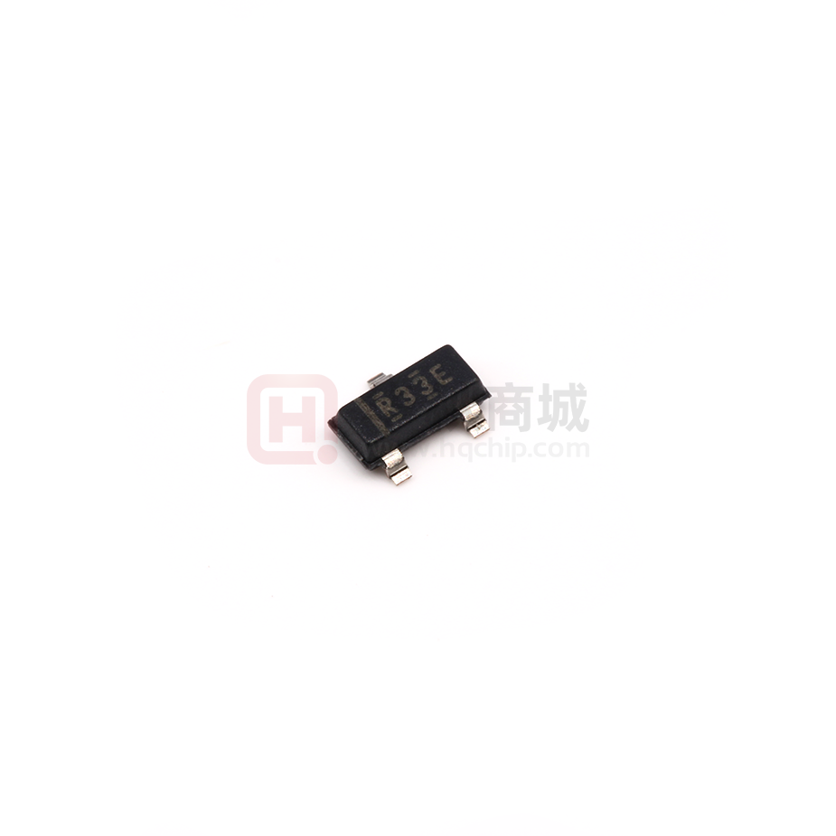
R33E
REF3330AIDBZT
ACTIVE
SOT-23
DBZ
3
250
RoHS & Green
NIPDAU
Level-2-260C-1 YEAR
-40 to 125
R33E
REF3330AIDBZTG4
ACTIVE
SOT-23
DBZ
3
250
RoHS & Green
NIPDAU
Level-2-260C-1 YEAR
-40 to 125
R33E
REF3330AIDCKR
ACTIVE
SC70
DCK
3
3000
RoHS & Green
NIPDAU
Level-2-260C-1 YEAR
-40 to 125
R30
REF3330AIDCKRG4
ACTIVE
SC70
DCK
3
3000
RoHS & Green
NIPDAU
Level-2-260C-1 YEAR
-40 to 125
R30
REF3330AIDCKT
ACTIVE
SC70
DCK
3
250
RoHS & Green
NIPDAU
Level-2-260C-1 YEAR
-40 to 125
R30
REF3330AIDCKTG4
ACTIVE
SC70
DCK
3
250
RoHS & Green
NIPDAU
Level-2-260C-1 YEAR
-40 to 125
R30
REF3330AIRSER
ACTIVE
UQFN
RSE
8
5000
RoHS & Green
NIPDAU
Level-1-260C-UNLIM
-40 to 125
EN
REF3333AIDBZR
ACTIVE
SOT-23
DBZ
3
3000
RoHS & Green
NIPDAU
Level-2-260C-1 YEAR
-40 to 125
R33F
REF3333AIDBZT
ACTIVE
SOT-23
DBZ
3
250
RoHS & Green
NIPDAU
Level-2-260C-1 YEAR
-40 to 125
R33F
REF3333AIDCKR
ACTIVE
SC70
DCK
3
3000
RoHS & Green
NIPDAU
Level-2-260C-1 YEAR
-40 to 125
R33
REF3333AIDCKT
ACTIVE
SC70
DCK
3
250
RoHS & Green
NIPDAU
Level-2-260C-1 YEAR
-40 to 125
R33
Addendum-Page 2
Samples
�PACKAGE OPTION ADDENDUM
www.ti.com
Orderable Device
13-Aug-2021
Status
(1)
Package Type Package Pins Package
Drawing
Qty
Eco Plan
(2)
Lead finish/
Ball material
RoHS & Green
NIPDAU
MSL Peak Temp
Op Temp (°C)
Device Marking
(3)
(4/5)
(6)
REF3333AIDCKTG4
ACTIVE
SC70
DCK
3
250
Level-2-260C-1 YEAR
-40 to 125
R33
(1)
The marketing status values are defined as follows:
ACTIVE: Product device recommended for new designs.
LIFEBUY: TI has announced that the device will be discontinued, and a lifetime-buy period is in effect.
NRND: Not recommended for new designs. Device is in production to support existing customers, but TI does not recommend using this part in a new design.
PREVIEW: Device has been announced but is not in production. Samples may or may not be available.
OBSOLETE: TI has discontinued the production of the device.
(2)
RoHS: TI defines "RoHS" to mean semiconductor products that are compliant with the current EU RoHS requirements for all 10 RoHS substances, including the requirement that RoHS substance
do not exceed 0.1% by weight in homogeneous materials. Where designed to be soldered at high temperatures, "RoHS" products are suitable for use in specified lead-free processes. TI may
reference these types of products as "Pb-Free".
RoHS Exempt: TI defines "RoHS Exempt" to mean products that contain lead but are compliant with EU RoHS pursuant to a specific EU RoHS exemption.
Green: TI defines "Green" to mean the content of Chlorine (Cl) and Bromine (Br) based flame retardants meet JS709B low halogen requirements of


 工商网监
湘ICP备2023018690号
工商网监
湘ICP备2023018690号
