REG1117
REG1117A
SBVS001D − OCTOBER 1992 − REVISED JULY 2004
800mA and 1A Low Dropout Positive Regulator
1.8V, 2.5V, 2.85, 3.3V, 5V, and Adjustable
FEATURES
D FIXED AND ADJUSTABLE VERSIONS
D 2.85V MODEL FOR SCSI-2 ACTIVE
D
D
D
D
D
D
TERMINATION
OUTPUT CURRENT:
REG1117: 800mA max
REG1117A: 1A max
OUTPUT TOLERANCE: +1% max
DROPOUT VOLTAGE:
REG1117: 1.2V max at IO = 800mA
REG1117A: 1.3V max at IO = 1A
INTERNAL CURRENT LIMIT
THERMAL OVERLOAD PROTECTION
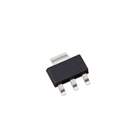
SOT-223 AND DDPAK SURFACE-MOUNT
PACKAGES
DESCRIPTION
The REG1117 is a family of easy-to-use three-terminal
voltage regulators. The family includes a variety of fixedand adjustable-voltage versions, two currents (800mA and
1A) and two package types (SOT-223 and DDPAK). See
the chart below for available options.
Output voltage of the adjustable versions is set with two
external resistors. The REG1117 low dropout voltage
allows its use with as little as 1V input-output voltage
differential.
Laser trimming assures excellent output voltage accuracy
without adjustment. An NPN output stage allows output
stage drive to contribute to the load current for maximum
efficiency.
800mA
VOLTAGE
APPLICATIONS
D
D
D
D
D
D
SOT-223
1A
DDPAK
1.8V
2.5V
SCSI-2 ACTIVE TERMINATION
HAND-HELD DATA COLLECTION DEVICES
HIGH EFFICIENCY LINEAR REGULATORS
BATTERY-POWERED INSTRUMENTATION
BATTERY MANAGEMENT CIRCUITS FOR
NOTEBOOK AND PALMTOP PCs
CORE VOLTAGE SUPPLY: FPGA, PLD, DSP,
CPU
2.85V
n
3.3V
n
5V
n
Adjustable
n
SOT-223
DDPAK
n
n
n
n
n
n
n
n
Please be aware that an important notice concerning availability, standard warranty, and use in critical applications of Texas Instruments
semiconductor products and disclaimers thereto appears at the end of this data sheet.
All trademarks are the property of their respective owners.
Copyright 1992−2004, Texas Instruments Incorporated
��������� �
�
��
�������� �� ������� �� �
����������� ����� ��������
���
��� �� �����
�������� ��� ��� ����� �
����� ����������� �������� ���������
���������� ���������! ���� ��� ����������� ������� ������! �
��� �����������
www.ti.com
��"#$$$%
�"#$$$%
www.ti.com
SBVS001D − OCTOBER 1992 − REVISED JULY 2004
ABSOLUTE MAXIMUM RATINGS(1)
Power Dissipation . . . . . . . . . . . . . . . . . . . . . . . . . . Internally Limited
Input Voltage . . . . . . . . . . . . . . . . . . . . . . . . . . . . . . . . . . . . . . . +15V
Operating Junction Temperature Range . . . . . . . . −40°C to +125°C
Storage Temperature Range . . . . . . . . . . . . . . . . . −65°C to +150°C
Lead Temperature (soldering, 10s)(2) . . . . . . . . . . . . . . . . . +300°C
(1) Stresses above these ratings may cause permanent damage.
(2) See Soldering Methods section.
This integrated circuit can be damaged by ESD. Texas
Instruments recommends that all integrated circuits be
handled with appropriate precautions. Failure to observe
proper handling and installation procedures can cause damage.
ESD damage can range from subtle performance degradation to
complete device failure. Precision integrated circuits may be more
susceptible to damage because very small parametric changes could
cause the device not to meet its published specifications.
CONNECTION DIAGRAM
Front View
Plastic SOT−223
Plastic DDPAK
Tab is
VOUT
Tab is VOUT
Ground VOUT
(Adj.)(1)
VIN
Ground VOUT
(Adj.)(1)
NOTE: (1) Adjustable−Voltage Model.
2
VIN
��"#$$$%
�"#$$$%
www.ti.com
SBVS001D − OCTOBER 1992 − REVISED JULY 2004
PACKAGE/ORDERING INFORMATION(1)
PRODUCT
VO/IO
PACKAGE-LEAD
PACKAGE
DESIGNATOR
OPERATING
TEMPERATURE
RANGE
PACKAGE
MARKING
REG1117-2.85
2.85/800mA
SOT223-3
DCY
−40°C to
+125°C
BB11172
REG1117-3.3
3.3/800mA
SOT223-3
DCY
−40°C to
+125°C
BB11174
KTT
−40 C to
−40°C
+125°C
REG1117F-3.3
3.3/800mA
DDPAK-3
REG1117-5
5V/800mA
SOT223-3
DCY
REG1117
Adj./800mA
SOT223-3
DCY
−40°C to
+125°C
BB1117
REG1117A-1.8
1.8V/1A
SOT223-3
DCY
−40°C to
+125°C
R111718
KTT
−40 C to
−40°C
+125°C
REG1117FA1.8
−40°C to
+125°C
R111725
REG1117A-2.5
REG1117FA-2.5
REG1117FA-5
REG1117A
REG1117FA
1.8/1A
2.5/1A
2.5/1A
5/1A
Adj./1A
Adj./1A
DDPAK-3
SOT223-3
DDPAK-3
DDPAK-3
SOT223-3
DDPAK-3
DCY
KTT
KTT
−40 C to
−40°C
+125°C
−40 C to
−40°C
+125°C
DCY
−40°C to
+125°C
KTT
−40 C to
−40°C
+125°C
BB11175
Rails, 80
REG1117-2.85
Tape and Reel,
2500
REG1117-3.3
Rails, 80
REG1117-3.3
Tape and Reel,
2500
REG1117F-3.3KTTT
Tape and Reel,
50
REG1117F-3.3/500
Tape and Reel,
500
REG1117-5
Rails, 80
REG1117-5
Tape and Reel,
2500
REG1117
Rails, 80
REG1117
Tape and Reel,
2500
REG1117A-1.8
Rails, 80
REG1117A-1.8
Tape and Reel,
2500
REG1117FA-1.8KTTT
Tape and Reel,
50
REG1117FA-1.8/500
Tape and Reel,
500
REG1117A-2.5
Rails, 80
REG1117A-2.5
Tape and Reel,
2500
REG1117FA-2.5KTTT
Tape and Reel,
50
REG1117FA-2.5/500
Tape and Reel,
500
REG1117FA-5/KTTT
Tape and Reel,
50
REG1117FA-5/500
Tape and Reel,
500
REG1117A
Rails, 80
REG1117A
Tape and Reel,
2500
REG1117FA/KTTT
Tape and Reel,
50
REG1117FA/500
Tape and Reel,
500
REG1117FA2.5
BB1117FA5.0
BB1117A
TRANSPORT
MEDIA,
QUANTITY
REG1117-2.85
BB1117F4
−40°C to
+125°C
REG1117FA-1.8
ORDERING
NUMBER
REG1117FA
(1) For the most current package and ordering information, see the Package Option Addendum located at the end of this data sheet.
3
��"#$$$%
�"#$$$%
www.ti.com
SBVS001D − OCTOBER 1992 − REVISED JULY 2004
ELECTRICAL CHARACTERISTICS
At TJ = +25°C, unless otherwise noted.
REG1117, REG1117A
PARAMETER
CONDITION
MIN
TYP
MAX
UNIT
REG1117-2.85
IO = 10mA, VIN = 4.85V
2.820
2.85
2.880
V
See Note 1
IO = 0 to 800mA, VIN = 4.05V to 10V
2.790
2.85
2.910
V
REG1117-3.3
IO = 10mA, VIN = 5.3V
3.270
3.30
3.330
V
See Note 1
IO = 0 to 800mA, VIN = 4.8V to 10V
3.240
3.30
3.360
V
IO = 10mA, VIN = 7V
4.950
5.00
5.050
V
See Note 1
IO = 0 to 800mA, VIN = 6.5V to 10V
4.900
5.00
5.100
V
REG1117A-1.8
IO = 10mA, VIN = 3.8V
1.782
1.8
1.818
V
OUTPUT VOLTAGE
REG1117-5
See Note 1
IO = 0 to 1A, VIN = 3.8V to 10V
1.764
1.8
1.836
V
REG1117A-2.5
IO = 10mA, VIN = 4.5V
2.475
2.5
2.525
V
See Note 1
IO = 0 to 1A, VIN = 4.5V to 10V
2.450
2.5
2.550
V
IO = 10mA, VIN = 7V
4.950
5.0
5.050
V
IO = 0 to 1A, VIN = 7V to 10V
4.900
5.0
5.100
V
IO = 10mA, VIN − VO = 2V
1.238
1.250
1.262
V
IO = 10 to 800mA, VIN − VO = 1.4 to 10V
1.225
1.250
1.280
V
IO = 10mA, VIN − VO = 2V
1.238
1.250
1.262
V
IO = 10mA to 1A, VIN − VO = 1.4 to 10V
1.225
1.250
1.280
V
IO = 0, VIN = 4.25 to 10V
1
7
mV
IO = 0, VIN = 4.8 to 10V
2
7
mV
IO = 0, VIN = 6.5 to 15V
3
10
mV
IO = 10mA, VIN − VO = 1.5 to 13.75V
0.1
0.4
%
REG1117A-5
See Note 1
REFERENCE VOLTAGE
REG1117 (Adjustable)
See Note 1
REG1117A (Adjustable)
See Note 1
LINE REGULATION
REG1117-2.85(1)
REG1117-3.3(1)
REG1117-5(1)
REG1117 (Adjustable)(1)
REG1117A (Adjustable)(1)
IO = 10mA, VIN − VO = 1.5 to 13.75V
0.1
0.4
%
REG1117A-1.8(1)
REG1117A-2.5(1)
IO = 0, VIN = 3.8V to 10V
1
7
mV
IO = 0, VIN = 4.5V to 10V
1
7
mV
REG1117A-5.0(1)
IO = 0, VIN = 7V to 15V
3
10
mV
IO = 0 to 800mA, VIN = 4.25V
2
10
mV
IO = 0 to 800mA, VIN = 4.8V
3
12
mV
LOAD REGULATION
REG1117-2.85(1)
REG1117-3.3(1)
REG1117-5(1)
IO = 0 to 800mA, VIN = 6.5V
3
15
mV
IO = 10 to 800mA, VIN − VO = 3V
0.1
0.4
%
IO = 10mA to 1A, VIN − VO = 3V
0.1
0.4
%
REG1117A-1.8(1)
IO = 0 to 1A, VIN = 3.8V
2
10
mV
REG1117A-2.5
IO = 0 to 1A, VIN = 4.5V
2
10
mV
REG1117A-5
IO = 0 to 1A, VIN = 7.0V
3
15
mV
IO = 100mA
1.00
1.10
V
IO = 500mA
1.05
1.15
V
IO = 800mA
1.10
1.20
V
IO = 1A
1.2
1.30
V
IO = 1A
1.2
1.55
V
REG1117 (Adjustable)(1)(2)
REG1117A (Adjustable)(1)(2)
DROPOUT VOLTAGE(3)
All Models(1)
See Note 1
REG1117 Models(1)
REG1117A
See Note 1
(1) Specification applies over the full specified junction temperature range, 0°C to +125°C.
(2) REG1117 and REG1117A adjustable versions require a minimum load current for ±3% regulation.
(3) Dropout voltage is the input voltage minus output voltage that produces a 1% decrease in output voltage.
(4) Percentage change in unloaded output voltage before versus after a 30ms power pulse of IO = 800mA (REG1117 models), IO = 1A (REG1117A),
VIN − VO = 1.4V (reading taken 10ms after pulse).
4
��"#$$$%
�"#$$$%
www.ti.com
SBVS001D − OCTOBER 1992 − REVISED JULY 2004
ELECTRICAL CHARACTERISTICS (continued)
At TJ = +25°C, unless otherwise noted.
REG1117, REG1117A
PARAMETER
CONDITION
MIN
TYP
MAX
UNIT
REG1117 Models
VIN − VO = 5V
800
950
1200
mA
REG1117A
VIN − VO = 5V
1000
1250
1600
mA
1.7
5
mA
CURRENT LIMIT
MINIMUM LOAD CURRENT
Adjustable Models(1)(2)
QUIESCENT CURRENT
Fixed-Voltage Models(1)
VIN − VO = 13.75V
VIN − VO = 5V
4
10
mA
IO = 10mA, VIN − VO = 1.4 to 10V
50
120
µA
IO = 10mA to 800mA, VIN − VO = 1.4 to 10V
0.5
5
µA
IO = 10mA to 1A, VIN − VO = 1.4 to 10V
0.5
5
µA
30ms Pulse
0.01
0.1
%/W
f = 120Hz, VIN − VOUT = 3V + 1VPP Ripple
62
dB
Fixed-Voltage Models
TJ = 0°C to +125°C
0.5
%
Adjustable Models
TJ = 0°C to +125°C
2
%
TA = 125°C, 1000Hr
0.3
%
f = 10Hz to 10kHz
0.003
%
15
°C/W
f > 50Hz
2
°C/W
dc
3
°C/W
65
°C/W
ADJUSTABLE PIN CURRENT(1)(2)
vs Load Current, REG1117(1)
vs Load Current, REG1117A(1)
THERMAL REGULATION
All Models(4)
RIPPLE REJECTION
All Models
TEMPERATURE DRIFT
LONG-TERM STABILITY
All Models
OUTPUT NOISE
rms Noise, All Models
THERMAL RESISTANCE
Thermal Resistance, qJC
(Junction-to-Case at Tab)
3-Lead SOT-223 Surface-Mount
3-Lead DDPAK Surface-Mount
Thermal Resistance, qJA
3-Lead DDPAK Surface-Mount
(Junction-to-Case at Tab)
No Heatsink
(1) Specification applies over the full specified junction temperature range, 0°C to +125°C.
(2) REG1117 and REG1117A adjustable versions require a minimum load current for ±3% regulation.
(3) Dropout voltage is the input voltage minus output voltage that produces a 1% decrease in output voltage.
(4) Percentage change in unloaded output voltage before versus after a 30ms power pulse of IO = 800mA (REG1117 models), IO = 1A (REG1117A),
VIN − VO = 1.4V (reading taken 10ms after pulse).
5
��"#$$$%
�"#$$$%
www.ti.com
SBVS001D − OCTOBER 1992 − REVISED JULY 2004
SIMPLIFIED SCHEMATIC
VIN
+
Current
Limit
Thermal
Limit
VOUT
10X
(Substrate)
Ground (Fixed−voltage Models)
Adj. (Adjustable−voltage Model)
6
��"#$$$%
�"#$$$%
www.ti.com
SBVS001D − OCTOBER 1992 − REVISED JULY 2004
TYPICAL CHARACTERISTICS
At TA = +25°C, all models, unless otherwise noted.
LOAD REGULATION
( ∆I LOAD = 800mA)
SHORT−CIRCUIT CURRENT vs TEMPERATURE
1
1300
REG1117A
1200
1100
REG1117 Models
1000
900
800
−50
−25
0
0
Output Voltage Deviation (mV)
Short−Circuit Current (mA)
1400
25
50
75
REG1117−2.85
1
REG1117A−1.8
−2
−3
−4
−5
REG1117−5
−6
−7
−50
100
−25
0
LINE REGULATION vs TEMPERATURE
VIN = 6.5V to 15V
REG1117−5
4
100
IOUT = 100mA
VRIPPLE = 1.0VPP
80
Ripple Rejection (dB)
Output Voltage Change (mV)
75
RIPPLE REJECTION vs FREQUENCY
90
5
3
2
1
REG1117A−1.8
VIN = 3.8V to 10V
0
70
60
50
40
30
20
−1
10
0
−25
0
25
50
75
100
10
100
1k
Temperature (_C)
10k
100k
Frequency (Hz)
QUIESCENT CURRENT vs TEMPERATURE
OUTPUT VOLTAGE vs TEMPERATURE
8
2.0
IO = 10mA
7
Fixed−Voltage Models
Quiescent Current (mA)
Output Voltage Change (%)
50
100
6
−2
−50
25
Temperature (_C)
Temperature (_ C)
1.0
0
−1.0
6
5
4
3
2
1
−2.0
−50
−25
0
25
50
Temperature (_ C)
75
100
0
−50
−25
0
25
50
75
100
Temperature (_C)
7
��"#$$$%
�"#$$$%
www.ti.com
SBVS001D − OCTOBER 1992 − REVISED JULY 2004
TYPICAL CHARACTERISTICS (continued)
At TA = +25°C, all models, unless otherwise noted.
LOAD TRANSIENT RESPONSE
LINE TRANSIENT RESPONSE
Output Voltage
Deviation (mV)
Output Voltage
Deviations (V)
60
0.1
0
−0.1
CIN = 1µF
COUT = 10µF Tantalum
IOUT = 0.1A
40
20
0
0
−0.5
0
20
40
60
80
100
Input Voltage (V)
Load Current (A)
−20
CIN = 10µF
COUT = 10µF
Tantalum
VIN = 4.25V
Preload = 0.1A
0.5
−40
5.25
4.25
3.25
0
20
40
60
Time (µs)
Time (µs)
Figure 2 shows a hookup diagram for the adjustable
voltage model. Resistor values are shown for some
commonly-used output voltages. Values for other voltages
can be calculated from the equation shown in Figure 2. For
best load regulation, connect R1 close to the output pin and
R2 close to the ground side of the load as shown.
APPLICATIONS INFORMATION
Figure 1 shows the basic hookup diagram for fixed-voltage
models. All models require an output capacitor for proper
operation, and for improving high-frequency load
regulation; a 10µF tantalum capacitor is recommended.
Aluminum electrolytic types of 50µF or greater can also be
used. A high-quality capacitor should be used to assure
that the ESR (Effective Series Resistance) is less than
0.5Ω.
VIN
THERMAL CONSIDERATIONS
The REG1117 has current limit and thermal shutdown
circuits that protect it from overload. The thermal shutdown
activates at approximately TJ = 165°C. For continuous
operation, however, the junction temperature should not
be allowed to exceed 125°C. Any tendency to activate the
thermal shutdown in normal use is an indication of an
inadequate heat sink or excessive power dissipation. The
power dissipation is equal to:
VO
REG1117
+
10µF
Tantalum
80 100 120 140 160 180 200
+ 10µF
Tantalum
PD = (VIN – VOUT) IOUT
The junction temperature can be calculated by:
TJ = TA + PD (qJA)
where TA is the ambient temperature, and qJA is the
junction-to-ambient thermal resistance.
Figure 1. Fixed-Voltage Model—Basic
Connections
VIN
C1 +
10µF
3
REG1117
(Adj)
1
C3(1) +
10µF
VO
2
R1
+ C2
10µF
Load
R2
VO =
R1 + R2
R1
x (1.25V) + (50µA) (R2)
This term is negligible with
proper choice of values−see
table at right.
VOUT
(V )
R1
(Ω)(2)
R2
(Ω)(2)
1.25
1.5
2.1
2.85
3
3.3
5
10
Open
750
158
169
137
115
113
113
Short
147
107
215
191
187
340
787
NOTES: (1) C3 optional. Improves high−frequency line rejection. (2) Resistors are standard 1% values.
Figure 2. Adjustable-Voltage Model—Basic Connections
8
��"#$$$%
�"#$$$%
www.ti.com
SBVS001D − OCTOBER 1992 − REVISED JULY 2004
A simple experiment will determine whether the maximum
recommended junction temperature is exceeded in an
actual circuit board and mounting configuration: Increase
the ambient temperature above that expected in normal
operation until the device’s thermal shutdown is activated.
If this occurs at more than 40°C above the maximum
expected ambient temperature, then TJ will be less than
125°C during normal operation.
The internal protection circuitry of the REG1117 was
designed to protect against overload conditions. It was not
intended to replace proper heat sinking. Continuously
running the REG1117 into thermal shutdown will degrade
reliability.
LAYOUT CONSIDERATIONS
The DDPAK (REG1117F-3.3 and REG1117FA) is a
surface-mount power package that has excellent thermal
characteristics. For best thermal performance, the
mounting tab should be soldered directly to a circuit board
copper area, as shown in Figure 3. Increasing the copper
area improves heat dissipation. Figure 4 shows typical
thermal resistance from junction-to-ambient as a function
of the copper area.
3−Lead DDPAK(1)
0.2
0.085
0.45
0.51
All measurements
in inches.
0.155
0.05
0.10
NOTE: (1) For improved thermal performance increase
footprint area. See Figure 4 (Thermal Resistance vs
Circuit Board Copper Area).
Figure 3. DDPAK Footprint
THERMAL RESISTANCE vs
CIRCUIT BOARD COPPER AREA
Circuit Board Copper Area
Thermal Resistance, qJA (°C/W)
60
REG1117F
DDPAK Surface Mount Package
1oz copper
50
40
30
20
REG1117F
DDPAK Surface−Mount Package
10
0
1
2
3
4
5
Copper Area (inches2)
Figure 4. DDPAK Thermal Resistance versus Circuit Board Copper Area
9
��"#$$$%
�"#$$$%
www.ti.com
SBVS001D − OCTOBER 1992 − REVISED JULY 2004
The SOT-223 package derives heat sinking from
conduction through its copper leads, especially the large
mounting tab. These must be soldered to a circuit board
with a substantial amount of copper remaining, as shown
in Figure 5. Circuit board traces connecting the tab and the
leads should be made as large as practical. The mounting
tab of both packages is electrically connected to VOUT.
Total Area: 50 x 50mm
35 x 17 mm
16 x 10 mm
16 x 10 mm
Without backside copper: q
With solid backside copper: q
≈ 59_ C/W
JA ≈ 49_C/W
Table 1. SOT-223 qJA for Various Board
Configurations
TOTAL PC
BOARD
AREA
TOPSIDE(1)
COPPER
AREA
BACKSIDE
COPPER
AREA
SOT-223
THERMAL
RESISTANCE
JUNCTIONTO-AMBIENT
2500mm2
2500mm2
2500mm2
46°C/W
2500mm2
1250mm2
2500mm2
47°C/W
2500mm2
950mm2
2500mm2
49°C/W
2500mm2
2500mm2
0
51°C/W
2500mm2
1800mm2
0
53°C/W
1600mm2
600mm2
1600mm2
55°C/W
2500mm2
1250mm2
0
58°C/W
2500mm2
915mm2
0
59°C/W
1600mm2
600mm2
0
67°C/W
900mm2
340mm2
900mm2
72°C/W
900mm2
340mm2
0
85°C/W
JA
(1) Tab is attached to the topside copper.
Figure 5. SOT-223 Circuit Board Layout Example
SOLDERING METHODS
Other nearby circuit traces, including those on the back
side of the circuit board, help conduct heat away from the
device, even though they may not be electrically
connected. Make all nearby copper traces as wide as
possible and leave only narrow gaps between traces.
Both REG1117 packages are suitable for infrared reflow
and vapor-phase reflow soldering techniques. The high
rate of temperature change that occurs with wave
soldering or hand soldering can damage the REG1117.
Table 1 shows approximate values of qJA for various circuit
board and copper areas for the SOT-223 package. Nearby
heat dissipating components, circuit board mounting
conditions, and ventilation can dramatically affect the
actual qJA. Proper heat sinking significantly increases the
maximum power dissipation at a given ambient
temperature, as shown in Figure 6.
INSPEC Abstract Number: B91007604, C91012627.
Kelly, E.G. “Thermal Characteristics of Surface 5WK9Ω
Packages.” The Proceedings of SMTCON. Surface Mount
Technology Conference and Exposition: Competitive
Surface Mount Technology, April 3−6, 1990, Atlantic City,
NJ, USA. Abstract Publisher: IC Manage, 1990, Chicago,
IL, USA.
MAXIMUM POWER DISSIPATION
vs AMBIENT TEMPERATURE
Power Dissipation (Watts)
6
q JA = 27_ C/W
(4in2 one oz copper
mounting pad)
5
PD = (TJ (max) − TA) / q JA
TJ (max) = 150_ C
qJA = 46_ C/W
(2500mm2 topside and
backside copper)
4
DDPAK
SOT−223
3
qJA = 65_ C/W
(no heat sink)
2
qJA = 85_ C/W
(340mm2 topside copper,
no backside copper)
1
0
0
25
50
75
100
125
Ambient Temperature (_ C)
Figure 6. Maximum Power Dissipation versus Ambient Temperature
10
��"#$$$%
�"#$$$%
www.ti.com
SBVS001D − OCTOBER 1992 − REVISED JULY 2004
TERMPWR
5V
TERMPWR
110Ω
2.85V
1N5817
110Ω
2.85V
REG1117−2.85
10µF
5V
1N5817
REG1117−2.85
10µF
10µF
(Up to 27 Lines)
110Ω
10µF
110Ω
Figure 7. SCSI Active Termination Configuration
REG1117−5
In
VIN > 12V
10µF
REG1117−5
Out
+
5V to 10V
+
GND
In
VIN > 9.0V
100µF
10µF
+
Out
7.5V
+
GND
100µF
2.5VOUT
10µF
+
1kΩ
REF1004−2.5
Figure 8. Adjusting Output of Fixed Voltage Models
Figure 9. Regulator with Reference
REG1117−5
VIN
In
10µF
5.2V Line
5.0V Battery
Out
GND
+
50Ω
1kΩ
REG1117−5
In
6.5V
10µF
Out
GND
+
+
100µF
Figure 10. Battery Backed-Up Regulated Supply
REG1117−5
In
VIN
10µF
+
Out
GND
+
100µF
Floating Input
VOUT = −5V
Figure 11. Low Dropout Negative Supply
11
�PACKAGE OPTION ADDENDUM
www.ti.com
10-Dec-2022
PACKAGING INFORMATION
Orderable Device
Status
(1)
Package Type Package Pins Package
Drawing
Qty
Eco Plan
(2)
Lead finish/
Ball material
MSL Peak Temp
Op Temp (°C)
Device Marking
(3)
Samples
(4/5)
(6)
REG1117
ACTIVE
SOT-223
DCY
4
80
RoHS & Green
NIPDAU
Level-1-260C-UNLIM
-40 to 125
BB1117
REG1117-2.85
LIFEBUY
SOT-223
DCY
4
80
RoHS & Green
NIPDAU
Level-1-260C-UNLIM
-40 to 125
BB11172
REG1117-2.85/2K5
ACTIVE
SOT-223
DCY
4
2500
RoHS & Green
NIPDAU
Level-1-260C-UNLIM
-40 to 125
BB11172
REG1117-2.85G4
LIFEBUY
SOT-223
DCY
4
80
RoHS & Green
NIPDAU
Level-1-260C-UNLIM
-40 to 125
BB11172
REG1117-3.3
ACTIVE
SOT-223
DCY
4
80
RoHS & Green
NIPDAU
Level-1-260C-UNLIM
-40 to 125
BB11174
Samples
REG1117-3.3/2K5
ACTIVE
SOT-223
DCY
4
2500
RoHS & Green
NIPDAU
Level-1-260C-UNLIM
-40 to 125
BB11174
Samples
REG1117-3.3/2K5G4
ACTIVE
SOT-223
DCY
4
2500
RoHS & Green
NIPDAU
Level-1-260C-UNLIM
-40 to 125
BB11174
Samples
REG1117-3.3G4
ACTIVE
SOT-223
DCY
4
80
RoHS & Green
NIPDAU
Level-1-260C-UNLIM
-40 to 125
BB11174
Samples
REG1117-5
ACTIVE
SOT-223
DCY
4
80
RoHS & Green
NIPDAU
Level-1-260C-UNLIM
-40 to 125
BB11175
Samples
REG1117-5/2K5
ACTIVE
SOT-223
DCY
4
2500
RoHS & Green
NIPDAU
Level-1-260C-UNLIM
-40 to 125
BB11175
Samples
REG1117-5G4
ACTIVE
SOT-223
DCY
4
80
RoHS & Green
NIPDAU
Level-1-260C-UNLIM
-40 to 125
BB11175
Samples
REG1117/2K5
ACTIVE
SOT-223
DCY
4
2500
RoHS & Green
NIPDAU
Level-1-260C-UNLIM
-40 to 125
BB1117
Samples
REG1117/2K5G4
ACTIVE
SOT-223
DCY
4
2500
RoHS & Green
NIPDAU
Level-1-260C-UNLIM
-40 to 125
BB1117
Samples
REG1117A
LIFEBUY
SOT-223
DCY
4
80
RoHS & Green
NIPDAU
Level-1-260C-UNLIM
-40 to 125
BB1117A
REG1117A-1.8
ACTIVE
SOT-223
DCY
4
80
RoHS & Green
NIPDAU
Level-1-260C-UNLIM
-40 to 125
R111718
Samples
REG1117A-1.8/2K5
ACTIVE
SOT-223
DCY
4
2500
RoHS & Green
NIPDAU
Level-1-260C-UNLIM
-40 to 125
R111718
Samples
REG1117A-2.5
ACTIVE
SOT-223
DCY
4
80
RoHS & Green
NIPDAU
Level-1-260C-UNLIM
-40 to 125
R111725
Samples
REG1117A-2.5/2K5
ACTIVE
SOT-223
DCY
4
2500
RoHS & Green
NIPDAU
Level-1-260C-UNLIM
-40 to 125
R111725
Samples
REG1117A/2K5
ACTIVE
SOT-223
DCY
4
2500
RoHS & Green
NIPDAU
Level-1-260C-UNLIM
-40 to 125
BB1117A
Samples
REG1117F-3.3/500
LIFEBUY
DDPAK/
TO-263
KTT
3
500
RoHS & Green
Call TI | SN
Level-2-260C-1 YEAR
-40 to 125
REG1117F4
Addendum-Page 1
Samples
Samples
�PACKAGE OPTION ADDENDUM
www.ti.com
Orderable Device
10-Dec-2022
Status
(1)
Package Type Package Pins Package
Drawing
Qty
Eco Plan
(2)
Lead finish/
Ball material
MSL Peak Temp
Op Temp (°C)
Device Marking
(3)
Samples
(4/5)
(6)
REG1117FA-1.8KTTT
ACTIVE
DDPAK/
TO-263
KTT
3
50
RoHS & Green
Call TI | SN
Level-2-260C-1 YEAR
-40 to 125
REG
1117FA1.8
Samples
REG1117FA-2.5/500
ACTIVE
DDPAK/
TO-263
KTT
3
500
RoHS & Green
Call TI | SN
Level-2-260C-1 YEAR
-40 to 125
REG
1117FA2.5
Samples
REG1117FA-5.0/500
ACTIVE
DDPAK/
TO-263
KTT
3
500
RoHS & Green
Call TI | SN
Level-2-260C-1 YEAR
-40 to 125
REG
1117FA5.0
Samples
REG1117FA/500
ACTIVE
DDPAK/
TO-263
KTT
3
500
RoHS & Green
Call TI | SN
Level-2-260C-1 YEAR
-40 to 125
REG1117FA
Samples
REG1117FA1.8KTTTG3
ACTIVE
DDPAK/
TO-263
KTT
3
50
RoHS & Green
SN
Level-2-260C-1 YEAR
-40 to 125
REG
1117FA1.8
Samples
(1)
The marketing status values are defined as follows:
ACTIVE: Product device recommended for new designs.
LIFEBUY: TI has announced that the device will be discontinued, and a lifetime-buy period is in effect.
NRND: Not recommended for new designs. Device is in production to support existing customers, but TI does not recommend using this part in a new design.
PREVIEW: Device has been announced but is not in production. Samples may or may not be available.
OBSOLETE: TI has discontinued the production of the device.
(2)
RoHS: TI defines "RoHS" to mean semiconductor products that are compliant with the current EU RoHS requirements for all 10 RoHS substances, including the requirement that RoHS substance
do not exceed 0.1% by weight in homogeneous materials. Where designed to be soldered at high temperatures, "RoHS" products are suitable for use in specified lead-free processes. TI may
reference these types of products as "Pb-Free".
RoHS Exempt: TI defines "RoHS Exempt" to mean products that contain lead but are compliant with EU RoHS pursuant to a specific EU RoHS exemption.
Green: TI defines "Green" to mean the content of Chlorine (Cl) and Bromine (Br) based flame retardants meet JS709B low halogen requirements of