www.ti.com
Table of Contents
User’s Guide
RS-485 Half-Duplex Evaluation Module
Joe Fockler
ABSTRACT
This manual describes the RS-485 Half-Duplex Evaluation Module (EVM). This EVM helps designers evaluate
the device performance, supporting the fast development and analysis of data transmission systems using any
of the TI RS-485 half-duplex devices in an 8-pin SOIC package.
Table of Contents
1 Trademarks..............................................................................................................................................................................1
2 Overview..................................................................................................................................................................................2
3 EVM Setup and Precautions.................................................................................................................................................. 3
4 Powering Up the EVM and Taking Measurements...............................................................................................................5
4.1 Measurement Examples.................................................................................................................................................... 5
5 Revision History......................................................................................................................................................................8
1 Trademarks
All trademarks are the property of their respective owners.
SLLU173C – OCTOBER 2012 – REVISED SEPTEMBER 2021
Submit Document Feedback
Copyright © 2021 Texas Instruments Incorporated
RS-485 Half-Duplex Evaluation Module
1
�Overview
www.ti.com
2 Overview
TI RS-485 half-duplex devices in the 8-pin SOIC package have robust drivers and receivers in a small package
for demanding industrial applications. The bus pins are robust to ESD events, with high levels of protection
to Human-Body Model and IEC Contact Discharge specifications. These devices each combine a differential
driver and a differential receiver, which operate from a single power supply. The driver differential outputs and
the receiver differential inputs are connected internally to form a bus port suitable for half-duplex (two-wire bus)
communication, and all feature a wide common-mode voltage range making the devices suitable for multi-point
applications over long cable runs. TI's RS-485 devices are characterized for industrial applications.
Note
This EVM comes without a transceiver soldered on to the board. The user can order any TI halfduplex, 8-pin SOIC RS-485 transceiver and solder it down on the board for evaluation. The EVM Tools
Folder contains links to devices that work with this EVM. See http://www.ti.com/tool/rs485-hf-dplx-evm
for more information.
Using the SN65HVD888 with Bus Polarity Correction Feature
This EVM can support the SN65HVD888 half-duplex RS-485 transceiver with bus polarity correction (See Figure
2-1). The SN65HVD888 transceiver corrects a wrong bus signal polarity caused by a cross-wire fault. In order to
detect the bus polarity all three of the following conditions must be met:
• a failsafe biasing network must be implemented (at the controller node) to set logic reference and define the
signal polarity of the bus,
• a target node must have its receiver enabled and its driver disabled ( RE = DE = Low),
• the bus must be idling for the failsafe time, tFS-max.
After the failsafe time has passed, the polarity correction is complete and is applied to both, receive and transmit
channels. The status of the bus polarity is latched within the transceiver and maintained for subsequent data
transmissions.
Note: Data streams of consecutive 0’s or 1’s with durations exceeding tFS-min can accidently trigger a wrong
polarity correction and must be avoided.
Cross-wire
fault
Vcc
R
R
B
DE
D
A
D
RT
RT
RFS
A
B
A
POLCOR
RE
R
R
RFS
A
B
D
B
Controller
SN65HVD82
RE
DE
D
Target
SN65HVD888
R
R
D
D
POLCOR
R
RE
DE
Target
SN65HVD888
POLCOR
D
R
RE
DE
D
Target
SN65HVD888
Figure 2-1. Typical Applications Diagram
2
RS-485 Half-Duplex Evaluation Module
SLLU173C – OCTOBER 2012 – REVISED SEPTEMBER 2021
Submit Document Feedback
Copyright © 2021 Texas Instruments Incorporated
�www.ti.com
EVM Setup and Precautions
3 EVM Setup and Precautions
Figure 3-1 shows the schematic of the EVM. The EVM board has headers labeled from JMP1 to JMP14 (JMP5
is omitted) and two 3-pin terminal blocks labeled TB1 and TB2. These headers support device evaluation for a
wide range of system configurations.
Note
The examples in this document show a 3.3-V signal generator and a 3.3-V power supply unit.
Depending on the Texas Instruments RS-485 device chosen, the user may need to provide a 5-V
signal generator input and 5-V power supply.
•
•
•
Pin 1 (EARTH) is a second ground pin that allows applying an external voltage between GND and EARTH to
simulate common-mode voltage conditions.
Pin 2 (GND) is connected to the negative output or ground terminal of the PSU. This pin represents the
ground potential of the device-under-test and the entire EVM. It also connects to various jumpers on the
board.
Pin 3 (VCC) is connected to the positive output of a regulated power supply unit (PSU) as it represents the
positive supply voltage of the device-under-test and also connects to various jumpers on the board.
3PIN_TERMINAL_BLOCK
TB1
DUT_VCC
DUT_VCC
2
DUT_GND
EARTH_GND
VCM_A
JMP10
C8
DUT_GND
1
UNINSTALLED
2
Header 4x1
3
DUT_GND
EARTH_GND
4
DUT_VCC
VCM_B
VCM_B
JMP9
Header 4x1
1
EARTH_GND
2
3
4
C9
DUT_GND
UNINSTALLED
VCM_B
Header 4x1
DUT_GND
EARTH_GND
1k Ohms
BLUE LED Diode
DUT_GND
C1
1uF
C2
0.1uF
EARTH_GND
C4
1uF
C5
0.1uF
R10
0 Ohm
DUT_GND
JMP11
3
2
1
R_1
DUT_GND
R
RED LED Diode
D3
DUT_GND
Header 3x1
Header 4x1
R6
UNINSTALLED
2
1
2
3
4
C6
UNINSTALLED
EARTH_GND
EARTH_GND DUT_GND
DUT_VCC
JMP2
R11
1k Ohms
/RE
1
2
3
4
3
2
1
DUT_GND
Header 4x1
DUT_GND
EARTH_GND
R2
50 Ohms
EARTH_GND
3PIN_TERMINAL_BLOCK
JMP6 JMP7
R5
120 Ohm
1
2
3
4
C7
UNINSTALLED
1
2
3
4
DUT_GND
D2
GREEN LED Diode
R3
50 Ohms
1
2
3
Header 4x1
Header 4x1
DUT_GND
1
3
2
1
DUT_GND
VCC
B
A
GND
2
DE
R
/RE
DE
D
EARTH_GND
8
7
6
5
EARTH_GND
EARTH_GND
JMP13
1
2
3
4
C3
R14
1k Ohms
EARTH_GND
JMP3
B_2
SN65HVD7x
Header 3x1
DUT_VCC
R8
0 Ohm
0.01uF
U1
JMP12
1
2
3
4
DUT_VCC
B
DUT_GND
1
DUT_VCC
JMP1
JMP8
1
2
3
4
3
D1
1
1
R1
DUT_VCC
2
VCM_A
EARTH_GND
TB2
EARTH_GND
R9
A
A_2
R7
UNINSTALLED
0 Ohm
DUT_GND
Header 3x1
Header 4x1
EARTH_GND
VCM_A
EARTH_GND
EARTH_GND
DUT_VCC
JMP4
NOTE: R2, R3, R4 - DNI
JMP14
1
2
3
4
D
3
2
1
DUT_GND
Header 4x1
DUT_GND
R4
50 Ohms
Header 3x1
EARTH_GND
EARTH_GND
EARTH_GND
Figure 3-1. RS-485 Half-Duplex EVM Schematic
SLLU173C – OCTOBER 2012 – REVISED SEPTEMBER 2021
Submit Document Feedback
Copyright © 2021 Texas Instruments Incorporated
RS-485 Half-Duplex Evaluation Module
3
�EVM Setup and Precautions
www.ti.com
For the first measurements, ignore the common-mode simulation and connect EARTH to GND through a
wire-bridge between pin 1 and pin 2 of TB1.
PSU
3.3V
3
2
1
TB1
Figure 3-2. Bridging DUT_GND with EARTH_GND
While JMP2 to JMP4 are stimulation points, or headers through which the control and data signals for the RS485
Half-Duplex EVM are applied, JMP1, and JMP11 to JMP14 are probe points, or headers at which these signal
can be measured.
Note that the 50-Ω resistors, R2, R3, and R4, have the index n.a., indicating that these components are not
assembled. Because signal generators have a typical source impedance of 50 Ω, their output signal is twice the
required signal voltage, and assumes that the on-board 50-Ω resistors divide this voltage down to the correct
signal level.
Without these resistors; however, this voltage divider action is not accomplished, and the generator output
voltage must be reduced to match the VCC requirements of the RS-485 device.
Signal
Generator
Scope
3.3V
Ch1
Ch2
JMP4
1
2
3
4
VCC
JMP14
1
2
3
D - input
Figure 3-3. Example for Stimulus and Probe Points with JMP4 and JMP14
Figure 3-3 gives an example for entering a data signal into the driver section of the transceiver. The signal
output of the generator is adjusted to match the device VCC power supply requirements . The generator’s ground
terminal is connected with pin 3, and the signal output terminal with pin 2 of JMP4. The data signal is measured
through an oscilloscope with its signal input connected to pin 1 and its ground wire connected to pin 2 of JMP14.
The same setup applies to the DE and RE inputs through their corresponding headers JMP2 and JMP12 and
JMP3 and JMP13. JMP1 however, must not receive a signal stimulus. Like JMP11, it represents the receiver
output, R, of the half-duplex RS-485 device.
Instead of using signal generators, the EVM can directly interface to the micro controller I/O. Then the nonassembled 50-Ω resistors are of no concern. However, for proper operation, it must be assured that the
high-level input voltage VIH ≥ 2 V and the low-level input voltage VIL ≤ 0.8 V.
4
RS-485 Half-Duplex Evaluation Module
SLLU173C – OCTOBER 2012 – REVISED SEPTEMBER 2021
Submit Document Feedback
Copyright © 2021 Texas Instruments Incorporated
�www.ti.com
Powering Up the EVM and Taking Measurements
4 Powering Up the EVM and Taking Measurements
The generally recommended procedure for taking measurements is listed:
1.
2.
3.
4.
Install the required ground connections.
Connect the oscilloscope with the respective probe points you want to measure.
Adjust the power-supply to match the VCC requirements of the selected RS-485 device.
Adjust the generator outputs for a maximum output signal level, based on the VCC requirements of your
selected RS-485 device, or check the logic switching levels of the controller I/O.
5. Connect the power supply conductor with pin 3 of TB1 and observe the blue LED (D1) turning on.
6. Connect signal conductors from the controller or the generator with their corresponding EVM inputs at JMP2
to JMP4.
7. Logic high at the receiver output, R, will turn on the red LED (D3), and logic high at the driver input, D,
turns on the green LED (D2). If D is left open, an internal 100-kΩ pull-up resistor provides logic high instead.
However, due to the small input current, D2 will remain off.
4.1 Measurement Examples
Each of the following measurement examples show the equivalent circuit diagram and the corresponding EVM
setup. Only the measurement relevant headers and terminal blocks are shown, and not necessarily at their exact
location on the EVM.
1. Standard Transceiver Configuration
Normal transceiver operation requires both the driver and the receiver sections being active. Therefore, the
receiver enable pin ( RE) must be at logic low potential and the driver enable pin (DE) at logic high.
Transmit data entering at the D-input terminal appear as the differential output voltage (VOD = VA – VB) on
the bus wires, A and B. Via the active receiver, it is possible to sense the data traffic in transmit direction.
DUT_VCC
U1
Receive
Data
0V
3.3V
Transmit
Data
R
1
RE
2
7
DE
3
6
A
D
4
5
GND
8
Vcc
R8
B
B
B
0W
R5
120 W
VOD
R9
VB
A
0W
A
VA
Figure 4-1. Transceiver Configuration for Normal Operation
Figure 4-2 shows the corresponding EVM setup. EARTH and GND receive the same reference potential,
PSU-ground, through the wire-bridge from pin 1 to pin 2 at the terminal block, TB1, while pin 3 (VCC), in this
example, is connected to the 3.3-V output of a power-supply unit (PSU).
SLLU173C – OCTOBER 2012 – REVISED SEPTEMBER 2021
Submit Document Feedback
Copyright © 2021 Texas Instruments Incorporated
RS-485 Half-Duplex Evaluation Module
5
�Powering Up the EVM and Taking Measurements
www.ti.com
Signal
Generator
Scope
PSU1
3.3V
Ch1
Ch2
Ch3
3.3V
Ch4
TB1
VCC
3
1
2
3
4
VCC
VCC
DE
R
JMP3
2
1
2
3
4
JMP11
1
2
3
GND
VCC
/RE
EARTH
1
2
3
4
1
JMP2
JMP6
1
2
3
4
B
A
JMP4
JMP14
1
2
3
D
Figure 4-2. RS-485 Half-Duplex EVM Setup for Normal Transceiver Operation
The low potential for RE is provided by the wire-bridge from pin 2 to pin 3 at JMP2, and the high potential
for DE through a wire-bridge from pin 2 to pin 1 at JMP3. Data from the signal generator enter the board
at pin 2 and pin 3 of JMP4. This data is measured via channel 1, which is connected to pin 1 and pin 2 of
JMP14. Channel 2 measures the receive data at JMP11, and channels 3 and 4 the bus voltages, VA and VB,
at JMP6.
2. Operation Under Maximum Load
EIA-485 (RS-485) specifies three maximum load parameters: a maximum differential load of 60 Ω, a
maximum common-mode load of 375 Ω for each bus wire, and a receiver common-mode voltage range
from –7 V to +12 V. Figure 4-3 reflects these requirements through R5, R8, R9, and VCM. Note that under
maximum load conditions the transceiver must be capable of sourcing and sinking bus currents of up to 55
mA. The purpose of this test is to show the robustness of VOD over the entire common-mode voltage range
at maximum load.
DUT_VCC
U1
Receive
Data
0V
3.3V
Transmit
Data
R
1
RE
2
8
7
Vcc
B
B
DE
3
6
A
D
4
5
GND
R5
60 W
VOD
R8
375 W
R9
A
375 W
VCM = -7V to +12V
Figure 4-3. Configuration for Maximum Loading
While the cable connections of the signal generator and the oscilloscope remain the same as in the previous
example, the following board changes need to be implemented to reflect maximum load conditions:
• replace R5 (120-Ω default) with 60 Ω
• replace R8 and R9 (0-Ω default) with 375 Ω
• connect pin 2 of JMP7 with pin 1 and pin 3 with pin 4
6
RS-485 Half-Duplex Evaluation Module
SLLU173C – OCTOBER 2012 – REVISED SEPTEMBER 2021
Submit Document Feedback
Copyright © 2021 Texas Instruments Incorporated
�www.ti.com
•
Powering Up the EVM and Taking Measurements
replace the previous wire-bridge at TB1 with a second power supply unit (PSU2) and connect the ground
terminals of both, PSU1 and PSU2 with a wire-bridge, as shown in Figure 4-4.
Signal
Generator
Scope
PSU2
PSU1
VCM
3.3V
Ch4
Ch3
Ch2
3.3V
Ch1
TB1
VCC
JMP6
1
2
3
4
R8
375W
3
1
2
3
4
JMP3
2
VCC
DE
R
VCC
1
2
3
4
JMP11
1
2
3
GND
VCC
/RE
EARTH
1
2
3
4
1
JMP2
JMP7
1
2
3
4
R9
375W
JMP4
JMP14
1
2
3
D
Figure 4-4. RS-485 Half-Duplex EVM Setup for Maximum Loading
Note that Figure 4-4 only shows the wiring of PSU2 for positive common-mode voltages. For negative VCM,
connect the ground terminal of PSU2 with pin 1 of TB1 (EARTH), and the VCM-output of PSU2 with the
ground terminal of PSU1.
Scope
Signal
Generator
PSU1
3.3V
Ch4
Ch3
Ch2
3.3V
Ch1
TB1
B
A
2
3
1
3
A
B
2
2
B
A
3
1
PSU2
1
2
3
3.3V
EARTH
VCC
DE
1
2
3
4
JMP14
3
2
1
VCC
JMP4
4
3
2
1
DE
VCC
JMP3
4
3
2
1
/RE
VCC
JMP2
4
3
2
1
TB2
TB2
JMP6
1
2
3
4
GND
JMP3
D
VCC
R
VCC
JMP11
1
2
3
GND
VCC
/RE
EARTH
1
2
3
4
1
JMP2
TB1
Figure 4-5. RS-485 Half-Duplex EVM Configurations: Left as Receiver EVM, Right as Transmitter EVM
SLLU173C – OCTOBER 2012 – REVISED SEPTEMBER 2021
Submit Document Feedback
Copyright © 2021 Texas Instruments Incorporated
RS-485 Half-Duplex Evaluation Module
7
�Revision History
www.ti.com
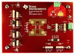
Figure 4-6. Top View of RS-485 Half-Duplex EVM
Figure 4-7. Bottom View of RS-485 Half-Duplex EVM
For detailed information on the device parameters see the data sheet of the selected device at www.ti.com
5 Revision History
NOTE: Page numbers for previous revisions may differ from page numbers in the current version.
Changes from Revision B (June 2013) to Revision C (September 2021)
Page
• Globally changed instances of legacy terminology to controller and target where mentioned........................... 1
8
RS-485 Half-Duplex Evaluation Module
SLLU173C – OCTOBER 2012 – REVISED SEPTEMBER 2021
Submit Document Feedback
Copyright © 2021 Texas Instruments Incorporated
�IMPORTANT NOTICE AND DISCLAIMER
TI PROVIDES TECHNICAL AND RELIABILITY DATA (INCLUDING DATA SHEETS), DESIGN RESOURCES (INCLUDING REFERENCE
DESIGNS), APPLICATION OR OTHER DESIGN ADVICE, WEB TOOLS, SAFETY INFORMATION, AND OTHER RESOURCES “AS IS”
AND WITH ALL FAULTS, AND DISCLAIMS ALL WARRANTIES, EXPRESS AND IMPLIED, INCLUDING WITHOUT LIMITATION ANY
IMPLIED WARRANTIES OF MERCHANTABILITY, FITNESS FOR A PARTICULAR PURPOSE OR NON-INFRINGEMENT OF THIRD
PARTY INTELLECTUAL PROPERTY RIGHTS.
These resources are intended for skilled developers designing with TI products. You are solely responsible for (1) selecting the appropriate
TI products for your application, (2) designing, validating and testing your application, and (3) ensuring your application meets applicable
standards, and any other safety, security, regulatory or other requirements.
These resources are subject to change without notice. TI grants you permission to use these resources only for development of an
application that uses the TI products described in the resource. Other reproduction and display of these resources is prohibited. No license
is granted to any other TI intellectual property right or to any third party intellectual property right. TI disclaims responsibility for, and you
will fully indemnify TI and its representatives against, any claims, damages, costs, losses, and liabilities arising out of your use of these
resources.
TI’s products are provided subject to TI’s Terms of Sale or other applicable terms available either on ti.com or provided in conjunction with
such TI products. TI’s provision of these resources does not expand or otherwise alter TI’s applicable warranties or warranty disclaimers for
TI products.
TI objects to and rejects any additional or different terms you may have proposed. IMPORTANT NOTICE
Mailing Address: Texas Instruments, Post Office Box 655303, Dallas, Texas 75265
Copyright © 2022, Texas Instruments Incorporated
�


 工商网监
湘ICP备2023018690号
工商网监
湘ICP备2023018690号