DS90UR905 Serializer and
DS90UR906 Deserializer
Evaluation Kit
User’s Manual
NSID: SERDESUR-65USB
Rev 0.4
National Semiconductor Corporation
Date: 3/26/2010
Page 1 of 44
�Table of Contents
TABLE OF CONTENTS ........................................................................................................................................... 2
INTRODUCTION: ..................................................................................................................................................... 3
CONTENTS OF THE DEMO EVALUATION KIT:.............................................................................................. 4
DS90UR905/906 SERDES TYPICAL APPLICATION:......................................................................................... 4
HOW TO SET UP THE DEMO EVALUATION KIT: .......................................................................................... 6
DEMO BOARD POWER CONNECTIONS:........................................................................................................... 6
DS90UR905 TX SERIALIZER BOARD DESCRIPTION: .................................................................................... 7
CONFIGURATION SETTINGS FOR THE TX DEMO BOARD ............................................................................................ 8
TX LVCMOS AND LVDS PINOUT BY CONNECTOR ................................................................................................ 13
BOM (BILL OF MATERIALS) SERIALIZER DEMO PCB: ........................................................................................... 14
DS90UR906 RX DE-SERIALIZER BOARD DESCRIPTION: ........................................................................... 14
CONFIGURATION SETTINGS FOR THE RX DEMO BOARD .......................................................................................... 16
RX LVDS PINOUT AND LVCMOS BY CONNECTOR ............................................................................................... 23
BOM (BILL OF MATERIALS) DE-SERIALIZER DEMO PCB:...................................................................................... 24
TYPICAL CONNECTION AND TEST EQUIPMENT........................................................................................ 25
TROUBLESHOOTING DEMO SETUP ................................................................................................................ 27
APPENDIX................................................................................................................................................................ 29
SERIALIZER (TX) DEMO PCB SCHEMATIC: ................................................................................................. 29
SERIALIZER (TX) DEMO PCB LAYOUT:......................................................................................................... 37
SERIALIZER (TX) DEMO PCB STACKUP:....................................................................................................... 40
DESERIALIZER (RX) DEMO PCB LAYOUT: ................................................................................................... 41
DESERIALIZER (RX) DEMO PCB STACKUP: ................................................................................................. 44
National Semiconductor Corporation
Date: 3/26/2010
Page 2 of 44
�Introduction:
The demo boards are not intended for EMI testing. The demo boards were
designed for easy accessibility to device pins with tap points for monitoring or
applying signals, additional pads for termination, and multiple connector options.
National Semiconductor’s Flat Panel Displays DS90UR905/906 FPD-LINKII evaluation
kit contains one (1) DS90UR905 Serializer (Tx) board, one (1) DS90UR906 Deserializer (Rx) board, and one (1) two (2) meter* high speed USB 2.0 cable. *Note: the
chipset can support up to ten (10) meters.
The DS90UR905/906 chipset supports a variety of 8 bit color display applications on a
two (2) wire serial stream. The single LVDS (FPD_LINKII) interface is well-suited for
any display system interface. Typical applications include: navigation displays,
automated teller machines (ATMs), POS, video cameras, global positioning systems
(GPS), portable equipment/instruments, factory automation, etc.
The DS90UR905 and DS90UR906 can also be used as a 24-bit general purpose LVDS
Serializer and De-serializer chipset designed to transmit data at clocks speeds ranging
from 20 to 65 MHz at up to 10 meters cable lengths over -40 to +105 Deg C.
The Serializer board accepts 1.8V/3.3V input signals. FPD-LINKII Serializer converts
the 1.8V/3.3V LVCMOS parallel lines into a single serialized LVDS data pair with an
embedded LVDS clock. The serial data stream toggles at 28 times the base clock rate.
With an input clock at 65 MHz, the transmission line rate for the FPD-LINKII is
1.56Gbps (24 data bits x 65MHz).
The De-serializer board accepts FPD-LINKII serialized data stream with embedded
clock and converts the data back into parallel 1.8V/3.3V LVCMOS signals and clock.
Note that NO external reference clock is needed to prevent harmonic lock as with other
devices currently on the market. An added feature on this chipset is when the PCLK
from the transmitter is lost; an internally generated 25MHz +/- 20% PCLK is outputted
on the receiver clock output. This feature can be turned off if not needed.
Suggested equipment to evaluate the chipset, a 1.8V/3.3V LVCMOS signal source such
as a video generator or word generator or pulse generator and oscilloscope with a
bandwidth of at least 65 MHz will be needed.
The user needs to provide the proper 1.8V/3.3V LVCMOS/RGB inputs and 1.8V/3.3V
LVCMOS clock to the Serializer and also provide a proper interface from the Deserializer output to an LCD panel or test equipment. The Serializer and De-serializer
boards can also be used to evaluate device parameters. A cable conversion board or
harness scramble may be necessary depending on type of cable/connector interface
used on the input to the DS90UR905 and to the output of the DS90UR906.
National Semiconductor Corporation
Date: 3/26/2010
Page 3 of 44
�Example of suggested display setup:
1) video generator with 1.8V/3.3V output
2) 24-bit LCD panel with a 1.8V/3.3V LVCMOS input interface.
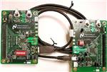
Contents of the Demo Evaluation Kit:
1) One Serializer board with the DS90UR905
2) One De-serializer board with the DS90UR906
3) One 2-meter high speed USB 2.0 cable (4-pin USB A to 5-pin mini USB)
4) Evaluation Kit Documentation (this manual)
5) DS90UR905/906 Datasheet
DS90UR905/906 SERDES Typical Application:
Figure 1a. Typical Application (24-bit RGB Color)
National Semiconductor Corporation
Date: 3/26/2010
Page 4 of 44
�Figure 1b. Typical DS90UR905/906 SERDES System Diagram
Figures 1a and 1b illustrate the use of the Chipset (Tx/Rx) in a Host to Flat Panel
Interface.
The chipsets support up to 24-bit color depth TFT LCD Panels.
Refer to the proper datasheet information on Chipsets (Tx/Rx) provided on each board
for more detailed information.
National Semiconductor Corporation
Date: 3/26/2010
Page 5 of 44
�How to set up the Demo Evaluation Kit:
The PCB routing for the Tx input pins (DIN) have been lay out to accept incoming
1.8V/3.3V LVCMOS signals from 2x25-pin IDC connector. The TxOUT/RxIN
(DOUT/RIN) interface uses a single twisted pair cable (provided). The PCB routing for
the Rx output pins (ROUT) are accessed through a 2x25-pin IDC connector. Please
follow these steps to set up the evaluation kit for bench testing and performance
measurements:
1) A two (2) meter high speed USB 2.0 cable has been included in the kit. Connect the
1
2
3
4
A
4-pin USB A
side of cable harness to the serializer board and the
otherside of the harness, the 5-pin mini USB jack 1 2 3 4
to the de-serializer
board. This completes the FPD-LINKII interface connection.
NOTE: The DS90UR905 and DS90UR906 are NOT USB compliant and should
not be plugged into a USB device nor should a USB device be plugged into the
demo boards.
MINI
2) Jumpers and switches have been configured at the factory; they should not require
any changes for immediate operation of the chipset. See text on Configuration
settings and datasheet for more details.
3) From the Video Decoder board, connect a flat cable (not supplied) to the Serializer
board and connect another flat cable (not supplied) from the De-serializer board to
the panel. Note: For 50 ohm signal sources, provide 1.8V/3.3V LVCMOS input
signal levels into DIN[23:0] and TCLK and add 50 ohm parallel termination resistors
R1-R25 on the DS90UR905 Serializer board.
4) Power for the Tx and Rx boards must be supplied externally through Power Jack
(VDD). Grounds for both boards are connected through Power Jack (VSS) (see
section below).
Demo Board Power Connections:
The Serializer and De-serializer boards must be powered by supplying power externally
through J4 (VDD) and J5 (VSS) on Serializer Board and J4 (VDD) and J5 (VSS) on Deserializer board. Note +2.5V is the MAXIMUM voltage that should ever be applied to
the Serializer (DS90UR905) or De-serializer (DS90UR906) VDD terminal (except on
VDDI or VDDIO where the absolute maximum is +4.0V). Damage to the device(s) can
result if the voltage maximum is exceeded.
National Semiconductor Corporation
Date: 3/26/2010
Page 6 of 44
�DS90UR905 Tx Serializer Board Description:
The 2x25-pin IDC connector J1 accepts 24 bits of 1.8V or 3.3V RGB data along with the
clock input. VDDI must be set externally for 1.8V or 3.3V LVCMOS inputs.
The Serializer board is powered externally from the J4 (VDD) and J5 (VSS) connectors
shown below. For the Serializer to be operational, the S1-PDB switch on S1 must be
set HIGH. S1- CONFIG0, CONFIG1, and BISTEN must be set LOW. Rising or falling
edge reference clock is user selected on S1-RFB: HIGH (for rising edge data latching)
or LOW (for falling edge data latching).
The USB connector P2 (USB-A side) on the bottom side of the board provides the
interface connection to the LVDS signals to the De-serializer board. Note: P1 (mini
USB) on the top side is un-stuffed and not to be used with the cable provided in the kit.
f J3, J4
f JP1
Note:
1) VDD and VSS applied
externally from J3 and J4
respectively.
2) To interface to 1.8V
inputs: place jumper
between pin 2 & 3 of JP2
(VDDI=+1.8V)
2b) To interface to 3.3V
inputs: place jumper
between pin 1 & 2 of JP2
and apply 3.3V on JP1
pin 1. (VDDI=+3.3V).
c FPD-LINKII OUTPUTS
d LVCMOS INPUTS
e FUNCTION CONTROLS
f POWER SUPPLY
1.8V
ONLY
g INPUT TERMINATION
(For 50Ω signal sources,
add 50Ω termination, otherwise
leave unpopulated)
e
JP5, VR3
J1
d
g
g
g
g
S1
Note:
Connect cable
(USB A side)
to P2 on BACKSIDE.
c P2 (BACKSIDE)
c P1 (TOPSIDE)
e
(UNSTUFFED)
National Semiconductor Corporation
Date: 3/26/2010
Page 7 of 44
�Configuration Settings for the Tx Demo Board
VDDI: 1.8V or 3.3V LVCMOS INPUT SELECTION
Reference
Description
VDDI LVCMOS input
JP2
VDDI = 1.8V
configuration.
(Default)
JP1
NOT USED
1.8V
ONLY
1.8V
LVCMOS
inputs
National Semiconductor Corporation
VDDI = 3.3V
apply external
1.8V
ONLY
3.3V
LVCMOS
inputs
Date: 3/26/2010
Page 8 of 44
�S1: Serializer Input Features Selection
Reference
Description
Input = L
RFB
Latch input data
Falling
on Rising or
Edge
Falling edge of
(Default)
TCLK
PDB
PowerDown Bar
Powers
Down
CONFIG0 See datasheet
MUST be
(* IMPORTANT
Table 2 for
tied low for
See user note
description of
normal
below)
features
operation
(Default)
CONFIG1 See datasheet
MUST be
(* IMPORTANT
Table
2
for
tied low for
See user note
description of
normal
below)
features
operation
(Default)
BISTEN
BIST ENable
OFF
See datasheet
(Default)
Table 2 for
description
VODSEL
FPD-LINKII output low
VOD SELect
(Default)
RES 2
(* IMPORTANT
See user note
below)
REServed
Input = H
Rising Edge
S1
Operational
(Default)
-
-
ON
high
MUST be
tied low for
normal
operation
(Default)
*Note:
In user layout CONFIG0 (pin 12), CONFIG1 (pin 13), RES 2 (pin 18) MUST be tied low
for proper operation.
National Semiconductor Corporation
Date: 3/26/2010
Page 9 of 44
�JP5,VR3: De-Emphasis Feature Selection
Reference
Description
JP5
OPEN
(floating)
Disabled –
no jumper
(Default)
De-Emphasis
CLOSED
(Path to GND)
Enabled –
With jumper
Note, when using
DeEmphasis, it is
recommended that
VODSEL = HIGH
CounterDe-Emphasis adjustment Clockwise
Clockwise
(via screw)
JP3 MUST have a jumper
to use VR3
decreases
potentiometer.
increases
RPRE value
RPRE value
VR3 = 0Ω to 20KΩ,
which
which
R1 = 1.5KΩ,
increases
decreases
R1 + VR3 =
De-emphasis
De1.5KΩ (maximum
emphasis
DeEmph) to
21.5KΩ (minimum
DeEmph).
IPRE = [1.2/(RDeEmph)] x 20,
RDeEmph (minimum) > 3KΩ
Note: There is no
maximum RDeEmph value
limitation
De-emphasis user note:
De-emphasis must be adjusted correctly based on application frequency, cable
quality, cable length, and connector quality. Maximum De-emphasis should only
be used under extreme worse case conditions; for example at the upper
frequency specification of the part and/or low grade cables at maximum cable
lengths. Typically all that is needed is minimum De-emphasis. Users should start
with no De-emphasis first and gradually apply De-emphasis until there is clock
lock and no data errors. The best way to monitor the De-emphasis effect is to
hook up a differential probe to RIN+ and RIN- on the DS90UR906 Rx demo. The
easiest tap point is pin2 of C1 and pin 2 of C2. The reason for monitoring RIN+/on the Rx side is because you want to see what the receiver will see the
attenuation signal AFTER the cable/connector.
JP5 &
VR3
National Semiconductor Corporation
Date: 3/26/2010
Page 10 of 44
�ID[x]J6,JP3: I2C like register programmable interface
Reference
Description
ID[x]=OPEN
(floating)
ID[x] I2C address
ID[x] = h’EC
ID[x]
RID thru
VR4
RID thru
external
resistor
RID
ID[x]
ID[x]
See RID
Counter clockwise
JP10 must have jumper
between pin 1 and pin 2 to
use VR4
RID value thru VR4
VR4 = 470Ω; ID[x]=h’E2
VR4 = 2.7KΩ; ID[x]=h’E4
VR4 = 8.2KΩ; ID[x]=h’E6
decreases RID value:
Clockwise increases
RID value
No jumper on JP10
RID value thru VR4
VR4 = 470Ω; ID[x]=h’E2
VR4 = 2.7KΩ; ID[x]=h’E4
VR4 = 8.2KΩ; ID[x]=h’E6
Clockwise
CounterClockwise
increases
RID value
decreases
RID value
De-emphasis
National Semiconductor Corporation
Date: 3/26/2010
Page 11 of 44
�JP13, JP14: USB Red and Black wire
Reference
Description
Power wire in USB cable
JP13
thru P2 (and P3, not
mounted) connector
Jumper RED to VSS –
recommended
JP14
Power wire in USB cable
thru P2 (and P3, not
mounted) connector
Jumper BLACK to VSS –
recommended
VDD
VSS
Red wire tied Red wire
tied to VSS
to VDD
(Default)
JP13
JP13
JP13
Black wire
tied to VDD
Black wire
tied to VSS
(Default)
JP14
JP14
OPEN
Red wire
floating
(not
recommended)
Black wire
floating
(not
recommended)
JP14
top side thru the board view
(mounted on solder side)
P2
pin 3
pin 4
USB A
BLACK WIRE
pin 2
+
_
pin 1
RED WIRE
National Semiconductor Corporation
Date: 3/26/2010
Page 12 of 44
�Tx LVCMOS and LVDS Pinout by Connector
The following three tables illustrate how the Tx inputs are mapped to the IDC connector
J1, the LVDS outputs on the USB-A connector P3, and the mini USB P2 (not mounted)
pinouts. Note – labels are also printed on the demo boards for both the LVCMOS input
and LVDS outputs.
J1
LVCMOS INPUT
pin no.
P2
(topside)
name
name
GND
R0
2
pin no.
name
3
GND
R1
4
1
JP13
pin no.
name
5
7
9
11
13
15
17
19
21
23
25
27
29
31
33
35
37
39
41
43
45
47
GND
R2
GND
R3
GND
R4
2
3
4
DOUT+
DOUTJP14
GND
R5
GND
R6
5
4
3
2
1
JP14
NC
DOUTDOUT+
JP13
GND
R7
GND
G0
GND
G1
GND
G2
GND
G3
GND
G4
GND
G5
GND
G6
GND
G7
GND
B0
GND
B1
GND
B2
GND
B3
GND
B4
GND
B5
GND
B6
GND
B7
6
8
10
12
14
16
18
20
22
24
26
28
30
32
34
36
38
40
42
44
46
48
49
GND
HS
50
51
GND
VS
52
53
GND
DE
54
55
GND
PCLK
56
1
pin no.
P3
(bottom side)
FPD-LinkII
OUTPUT
National Semiconductor Corporation
(not mounted)
FPD-LinkII
OUTPUT
Date: 3/26/2010
Page 13 of 44
�BOM (Bill of Materials) Serializer Demo PCB:
DS90UR905 Tx Demo Board - Board Stackup Revised: Thursday, June 18, 2009
DS90UR905 Tx Demo Board
Bill Of Materials
Item
Qty
1
Revision: 2
July 16,2009
19:47:16
PCB
Footprint
352821_EIA
CAP/HDC1206
CAP/HDC0603
CAP/HDC0603
Reference
Part
2
C1,C15
2.2uF
2
2
C16,C2
0.1uF
4
2
0.1uF
5
7
C5,C6
C7,C14,C20,C23,
C24,C28, C30
0.1uF
6
2
C10,C13
22uF
7
2
5pF
8
6
22uF
9
5
C11,C12
C17,C18,C21,C31,
C32,C33
C19,C25,C26,C27,
C29
0.01uF
CAP/N
CAP/HDC0201
CAP/EIA-B
3528-21
CAP/HDC0603
11
3
JP1,JP3,JP5
2-Pin Header
Header/2P
12
5
JP2,JP10,JP13,
JP14,JP15
3-Pin Header
Header/3P
16
1
J1
HEADER
28x2
18
2
J3,J4
BANANA
20
1
J6
IDC1X4
26
1
P3
USB A
27
1
1.50K
31
10
33
8
R1
R31,R32,R33,R45,
R46,R47,R48,R53,
R56,R57
R37,R58,R59,R60,
R61,R62, R63,R64
34
2
R40,R39
4.7K
38
2
R52,R51
0 ohm
RES/HDC0402
RES/HDC0603
RES/HDC0603
RES/HDC0201
2x28 0.1"
CON/
BANANA-S
IDC-1x4
USB_TYPE
_A_4P
RES/HDC0402
Comments
CAPACITOR TANT
2.2UF 20V 10% SMD
CAP .10UF 50V
CERAMIC X7R 1206
CAP CERAMIC .1UF
50V X7R 0603
CAP .1UF ±10% 25V
CERAMIC X7R 0603
CAP TANTALUM
22UF 25V 20% SMD
CAP CERAMIC 5.0PF
25V NP0 0201
CAPACITOR TANT
22UF 16V 20% SMD
CAP CERAMIC .01UF
100V X7R 0603
CONN HEADER
VERT .100 2POS
30AU
CONN HEADER
VERT .100 3POS
15AU
CONN HEADER
VERT 60POS .100
30AU. Cut to fit.
BANANA-female
(non-insulated)
CONN HEADER
4POS .100 VERT
GOLD
CONN USB RECEPT
R/A TYPE A 4POS.
RES 1.50K OHM
1/16W 1% 0402 SMD
39
1
S1
SW DIP-7
DIP-14
RES ZERO OHM
1/16W 5% 0402 SMD
RES 10.0K OHM
1/10W 1% 0603 SMD
RES 4.7K OHM
1/10W 5% 0603 SMD
RES 0.0 OHM 1/20W
5% 0201 SMD
SWITCH DIP
EXTENDED SEALED
7POS
40
1
U1
DS90UR905
44
1
VR3
SVR20K
45
1
VR4
SVR100K
48ld LLP
Surface
Mount 4mm
Square
Surface
Mount 4mm
Square
DS90UR905Q
11-Turn Trimming
Potentiometer; Top
Adjust
11-Turn Trimming
Potentiometer; Top
Adjust
0 Ohm, 0402
10K
National Semiconductor Corporation
MFR
MFR Part#
KEMET
T491B225K020AT
KEMET
C1206C104K5RACTU
Panasonic
ECJ-1VB1H104K
Panasonic
ECJ-1VB1E104K
nichicon
F931E226MNC
Panasonic
ECJ-ZEC1E050C
Kemet
T494B226M016AT
KEMET
C0603C103K1RACTU
AMP/Tyco
87220-2
AMP/Tyco
87224-3
AMP/TYCO
3-87215-0
Johnson
Molex/Waldom
Electronics
Corp
108-0740-001
AMP/Tyco
292303-1
Panasonic
ERJ-2RKF1501X
Panasonic
ERJ-2GEJ0R00X
Panasonic
ERJ-3EKF1002V
Panasonic
ERJ-3GEYJ472V
Panasonic
ERJ-1GE0R00C
22-11-2042
Grayhill
78B07ST
National
DS90UR905Q
Bourns
3224W-1-203E
Bourns
3224W-1-104E
Date: 3/26/2010
Page 14 of 44
�DS90UR906 Rx De-serializer Board Description:
The USB connector J2 (mini USB) on the topside of the board provides the interface
connection for FPD-LINKII signals to the Serializer board. Note: J3 (mini USB) on the
bottom side is un-stuffed and not used with the cable provided in the kit.
The De-serializer board is powered externally from the J9 (VDD) and J7 (VSS)
connectors shown below. For the De-serializer to be operational, the S1 – SLEEPB and
switche on S1 must be set HIGH. Rising or falling edge reference clock is user selected
by S1-RRFB: HIGH (for rising edge strobing) or LOW (for falling edge strobing).
The 2x25 pin IDC Connector P1 provides access to the 24 bit 1.8V or 3.3V LVCMOS
and clock outputs.
f J4, J5
f J4, J5, JP1
Note:
1) VDD and VSS applied
externally from J4 and J5
respectively.
2) To interface to 1.8V inputs:
place jumper between pin 2 &
3 of JP2 (VDDIO=+1.8V)
2b) To interface to 3.3V inputs:
place jumper between pin 1 &
2 of JP2 and apply 3.3V on
JP1 pin 1. (VDDIO=+3.3V).
1.8V
ONLY
d JP8
d P1
d JP9
e S1
c FPD-LINKII INPUTS
d LVCMOS OUTPUTS
e FUNCTION CONTROLS
f POWER SUPPLY
Note:
Connect cable
(mini USB side) to J2
on (TOPSIDE).
c J2 (TOPSIDE)
c J3 (BACKSIDE)
(UNSTUFFED)
National Semiconductor Corporation
Date: 3/26/2010
Page 15 of 44
�Configuration Settings for the Rx Demo Board
VDDIO: 1.8V or 3.3V LVCMOS INPUT/OUTPUT SELECTION
Reference
Description
VDDIO = 1.8V
VDDIO = 3.3V
VDDIO LVCMOS
JP1
apply
(Default)
input/output configuration.
externally
1.8V
ONLY
1.8V
LVCMOS
National Semiconductor Corporation
1.8V
ONLY
3.3V
LVCMOS
Date: 3/26/2010
Page 16 of 44
�S1, STRAPS: De-serializer Input Features Selection
Reference
Description
Input = L
Input = H
PDB
PowerDown Bar
Power
Operational
Down
(Default)
(Disabled)
BISTEN
BIST ENable
OFF
ON
See datasheet Table (Default)
2 for description
Note: Set BISTEN on
the DS90UR905
before the
DS90UR906
RES0
REServed
MUST be
(* IMPORTANT
tied low for
See user note
normal
below)
operation
(Default)
S1
*Note: In user layout RES0 (pin 47) MUST be tied low for proper operation.
National Semiconductor Corporation
Date: 3/26/2010
Page 17 of 44
�STRAPs: De-serializer Input Features Selection
There are two options for setting strap(s):
1) On-the-fly strap selection on the demo board is a six (6) step process:
Step 1: Set PDB to LOW on SW1.
mode.
This will place the part in power down
Step 2: Place jumper between pin 1 and 2 of JP18.
This ties the even numbered pins on P1 to VDDIO which will provide the
pullup for the strap option.
VDDIO
Step 3: Place jumper(s) on strap pins option(s) desired.
E.g. if you wanted to change RDS from default RDS=L (low drive strength)
to RDS=H (high drive strength), place a jumper on RDS of P1.
Step 4: Switch PDB on SW1 from LOW to HIGH.
This overrides the default
register(s) and will place the part in normal operating mode.
Step 5: Remove ALL jumper(s) on strap pin placed in Step 3.
Step 6: Remove jumper between pin 1 and 2 of JP18 and place the jumper between
pin 2 and 3 of JP18.
This ties the even numbered pins on P1 to VSS and is used as the ground
reference for R[7:0], G[7:0], B[7:0], HS, VS, DE, PCLK under normal
operating conditions.
VSS
National Semiconductor Corporation
Date: 3/26/2010
Page 18 of 44
�2) For straps options to be loaded permanently without using the on-the-fly option:
Place a 10K ohm 0201 size resistor on corresponding resistor pads.
E.g.
Note: This is the same configuration setting as previous example using 10K ohm resistor instead of jumpers
0201
R1
10Kohm_open
0201
R2
10Kohm_open
0201
R3
10Kohm_open
0201
R4
10Kohm_open
0201
R5
10Kohm_open
0201
R6
10Kohm_open
0201
R7
10Kohm_open
0201
R8
10Kohm_open
0201
R9
10Kohm_open
0201 R10
10Kohm_open
0201 R11
10Kohm_open
0201 R12
10Kohm_open
0201 R13
10Kohm_open
0201 R14
10Kohm_open
0201 R15
10Kohm_open
0201 R16
10Kohm_open
0201 R17
10Kohm_open
0201 R18
10Kohm_open
0201 R19
10Kohm_open
0201 R20
10Kohm_open
0201 R21
10Kohm_open
0201 R22
10Kohm_open
0201 R23
10Kohm_open
0201 R24
10Kohm_open
0201 R25
10Kohm_open
0201 R26
10Kohm_open
0201 R27
10Kohm_open
0201 R28
10Kohm_open
VD D IOc
P1
M A P0
M A P1
SSC 0
SSC 1
SSC 2
SSC 3
OSC 0
OSC 1
OSC 2
EQ0
EQ1
EQ2
EQ3
R FB
OSS
RDS
LFM
C F1
C F0
-
1
3
5
7
9
11
13
15
17
19
21
23
25
27
29
31
33
35
37
39
41
43
45
47
49
51
53
55
HEADER 28x2
R0
R1
R2
R3
R4
R5
R6
R7
G0
G1
G2
G3
G4
G5
G6
G7
B0
B1
B2
B3
B4
B5
B6
B7
HS
VS
DE
PCLK
R0
R1
R2
R3
R4
R5
R6
R7
G0
G1
G2
G3
G4
G5
G6
G7
B0
B1
B2
B3
B4
B5
B6
B7
HS
VS
DE
PCLK
2
4
6
8
10
12
14
16
18
20
22
24
26
28
30
32
34
36
38
40
42
44
46
48
50
52
54
56
JP18
VD D IOc 1
ST R A P 2
VSS 3
Normal
operation
For strap
pullup
Ties all even pins
on P1 to HIGH or
LOW.
All strap inputs = L
Strap pullup to
VDDIO
National Semiconductor Corporation
Date: 3/26/2010
Page 19 of 44
�Reference
Description
MAPSEL[1:0] MAP SELect
Input = L
Input = H
P1
(Default)
No jumpers
SSC[3:0]
Spread Spectrum
Clock Generation
control
See datasheet for
settings
Disabled
(Default)
No jumpers
(15 settings)
OSC[2:0]
EQ[0]
OSCillator
Frequency select
See datasheet for
settings
Equalizer
Disable/Enable
Disabled
(Default)
No jumpers
Disabled
(7 settings)
Enabled
(Default)
No jumper
EQ[3:1]
RFB
OSS SEL
RDS
EQualizer control
See datasheet for
settings
Latch output data
on Rising or Falling
Data Strobe of
RCLK
Output Select Sleep
SELect
Reciever Output
Drive Strength
(Default)
No jumpers
Falling
Rising
(Default)
No jumper
Disabled
Must also set JP18
(Default)
No jumper
Low drive
strength
Enabled
High drive
strength
(Default)
National Semiconductor Corporation
Date: 3/26/2010
Page 20 of 44
�LF_MODE
CONFIG[1:0]
Low Frequency
MODE
Used only when
SSCG is enabled
otherwise this pin is
a don’t care
CONFIGuration
control
See datasheet for
settings
No jumper
PCLK>20MHz PCLK