SM28VLT32-HT
www.ti.com
SLVSAO2C – NOVEMBER 2012 – REVISED MARCH 2013
32-MBIT HIGH-TEMPERATURE FLASH MEMORY
WITH SERIAL PERIPHERAL INTERFACE (SPI) BUS
Check for Samples: SM28VLT32-HT
FEATURES
1
•
•
•
•
•
•
•
•
•
•
•
32-Megabit Flash for High-Temperature
Applications
Serial Peripheral Interface (SPI) Compatible
(Mode 0 and 3)
3.3-V Supply for IO, 1.9 V for Core
2-M x 16-Bit Word Access
Asynchronous Read, Write, and Erase
Operations
Erase Operation Supported Only for -55°C to
125°C
12-MHz Maximum Clock Frequency
Endurance: 1000 Program and Erase Cycles
Data Retention: 1000 hrs
ESD Protection: 2-kV HBM, 500-V CDM
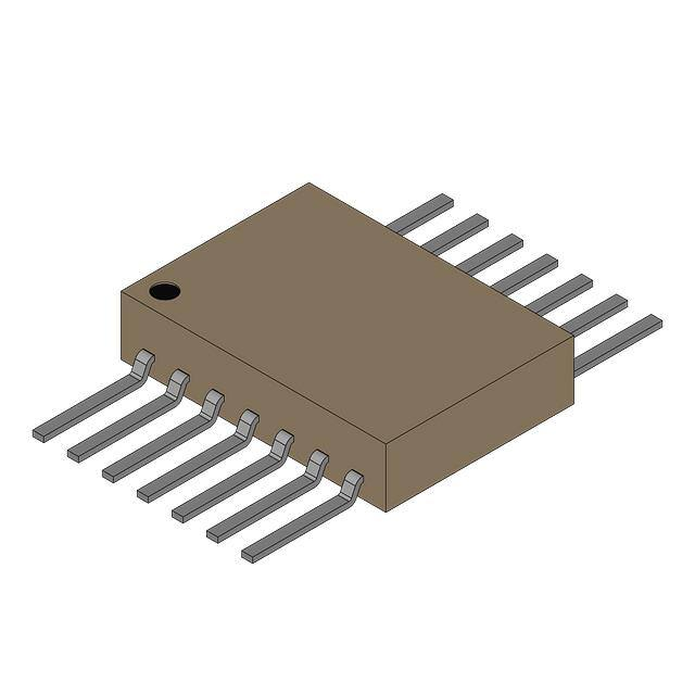
8-mm x 20-mm 14-Pin Ceramic HKN Package
and KGD (Bare Die) Package
SUPPORTS EXTREME TEMPERATURE
APPLICATIONS
•
•
•
•
Controlled Baseline
One Assembly and Test Site
One Fabrication Site
Available in Extreme (–55°C to 210°C)
Temperature Range (1)
Extended Product Life Cycle
Extended Product-Change Notification
Product Traceability
Texas Instruments high temperature products
utilize highly optimized silicon (die) solutions
with design and process enhancements to
maximize performance over extended
temperatures. All devices are characterized
and qualified for 1000 hours continuous
operating life at maximum rated temperature.
•
•
•
•
APPLICATIONS
•
•
•
•
Down-Hole Energy Drilling
Test and Measurement Equipment
Seismic Data Collection at Extreme
Temperatures
General Data Collection Applications at
Extreme High- and Low-Temperatures
HKN PACKAGE
(TOP VIEW)
VSS
HOLD#
VCORE
VIO
CS#
RST#
WP#
SO
SI
FLCLK
VIO
SCK
VSS
VCORE
(1)
Custom temperature ranges available
DESCRIPTION
SM28VLT32 is a 32-Megabit Flash Memory designed to store program code and/or data from acquisition. The
wide temperature rating of this device makes it ideal for applications that need to perform reliably in harsh
environments. SM28VLT32 with its serial peripheral interface (SPI) offers low pin count for additional reliability
and easy assembly in these applications.
The memory is partitioned as sectors to provide addressing of 2-M words of 16 bits each. Thus, the memory
address is 21 bits wide.
SM28VLT32 supports serial peripheral interface to read/write/erase data in the flash memory. The interface is
compliant with mode 0 (CPOL = 0, CPHA = 0) and 3 (CPOL = 1, CPHA = 1). Asserting CS# enables the device
to enter communication mode. With CS# de-asserted, the device ignores all activity on the SPI pins. As shown in
Figure 1, multiple SM28VLT32 devices can be controlled from a single Master by independently controlling CS#
pins in order to realize larger memory in the application. Asserting the HOLD# pin (while CS# is also asserted)
will let the device ignore activity on the other SPI input pins (SCK and SI).
1
Please be aware that an important notice concerning availability, standard warranty, and use in critical applications of
Texas Instruments semiconductor products and disclaimers thereto appears at the end of this data sheet.
PRODUCTION DATA information is current as of publication date.
Products conform to specifications per the terms of the Texas
Instruments standard warranty. Production processing does not
necessarily include testing of all parameters.
Copyright © 2012–2013, Texas Instruments Incorporated
�SM28VLT32-HT
SLVSAO2C – NOVEMBER 2012 – REVISED MARCH 2013
www.ti.com
SM28VLT32
SM28VLT32
SM28VLT32
SM28VLT32
CS#
SCK SI SO
CS#
SCK SI SO
CS#
SCK SI SO
CS#
SCK SI SO
SCK
SI
SO
CS1#
SPI Bus CS2#
Master / CS3#
Micro- CS4#
Controller
Figure 1. System Block Diagram That Shows Configuration to Use Multiple SM28VLT32 Devices to
Realize Larger Memory
The SM28LVT32 supports a hardware data protection scheme using the WP# pin. Erase and program
operations are inhibited if WP# is low.
2
Submit Documentation Feedback
Copyright © 2012–2013, Texas Instruments Incorporated
Product Folder Links: SM28VLT32-HT
�SM28VLT32-HT
www.ti.com
SLVSAO2C – NOVEMBER 2012 – REVISED MARCH 2013
This integrated circuit can be damaged by ESD. Texas Instruments recommends that all integrated circuits be handled with
appropriate precautions. Failure to observe proper handling and installation procedures can cause damage.
ESD damage can range from subtle performance degradation to complete device failure. Precision integrated circuits may be more
susceptible to damage because very small parametric changes could cause the device not to meet its published specifications.
ORDERING INFORMATION (1)
TJ
–55°C to 210°C
(1)
PACKAGE
ORDERABLE PART NUMBER
TOP-SIDE MARKING
14-Pin HKN
SM28VLT32SHKN
28VLT32SHKN
KGD (Bare Die)
SM28LVT32SKGD3
N/A
For the most current package and ordering information, see the Package Option Addendum at the end of this document, or see the TI
web site at www.ti.com.
ABSOLUTE MAXIMUM RATINGS (1)
over operating free-air temperature range (unless otherwise noted)
UNIT
VIO
Supply voltage range (for IO)
VCORE
Supply voltage range (for Core)
VI
Input voltage range
–0.2 V to (VIO + 0.2)
VO
Output voltage range
–0.2 V to (VIO + 0.2)
ESD
Electrostatic discharge (HBM, 1.5 kΩ, 100 pF)
TJ
Operating junction temperature range
(1)
–0.3 V to 4.5 V
–0.3 V to 2.5 V
> 2000 V
–55°C to 215°C
Stresses beyond those listed under absolute maximum ratings may cause permanent damage to the device. These are stress ratings
only and functional operation of the device at these or any other conditions beyond those indicated under recommended operating
conditions is not implied. Exposure to absolute-maximum-rated conditions for extended periods may affect device reliability.
PACKAGE DISSIPATION RATINGS
PACKAGE
θJA THERMAL IMPEDANCE
JUNCTION TO AMBIENT
θJC THERMAL IMPEDANCE
JUNCTION TO CASE (THERMAL PAD)
θJB THERMAL IMPEDANCE
JUNCTION TO BOARD
HKN
63°C/W
0.84°C/W
55°C/W
RECOMMENDED OPERATING CONDITIONS
MIN
TYP
MAX
VIO
Device supply voltage for IO
3.1
3.3
3.6
UNIT
VCORE
Device supply voltage for Core
1.8
1.9
1.98
V
TJ
Junction temperature
–55
210
°C
V
ELECTRICAL CHARACTERISTICS: IO
VIO = 3.1 V to 3.6 V, VCore = 1.8 V to 1.98 V, TJ = –55°C to 210°C (unless otherwise noted)
PARAMETER
TEST CONDITIONS
VIH
Input high voltage
VIL
Input low voltage
IOH
Output high current
VOH = VOHmin
IOL
Output low current
VOL = VOLmax
VOH
Output high voltage
IOH = IOHmin
VOL
Output low voltage
IOL = IOLmax
CI
Input capacitance
MIN
TYP
MAX
UNIT
2.5
V
0.9
-8
8
2.8
Submit Documentation Feedback
Product Folder Links: SM28VLT32-HT
mA
V
0.8
6.5
Copyright © 2012–2013, Texas Instruments Incorporated
V
mA
V
pF
3
�SM28VLT32-HT
SLVSAO2C – NOVEMBER 2012 – REVISED MARCH 2013
www.ti.com
ELECTRICAL CHARACTERISTICS: MEMORY
VIO = 3.1 V to 3.6 V, VCore = 1.8 V to 1.98 V, TJ = –55°C to 210°C (unless otherwise noted)
PARAMETER
tLife
TEST CONDITIONS
Continuous operating life
MIN
MAX
UNIT
127
160
mA
14
22
mA
1000
IDDVCORE
IDDVIO
Erase current
-55°C to 125°C
hrs
76
Program current
mA
85
Sector erase time
-55°C to 125°C
Program time 1 16-bit word
Nf
TYP
Flash endurance for the array
(write/erase cycles)
TJ = 30°C
mA
2
3
s
30
300
µs
1000
cycles
ELECTRICAL CHARACTERISTICS: SPI (1) (2)
VIO = 3.1 V to 3.6 V, VCore = 1.8 V to 1.98 V, TJ = –55°C to 210°C (unless otherwise noted)
PARAMETER
TEST CONDITIONS
MIN
TYP
(3)
MAX
UNIT
10
MHz
12
MHz
fSCK
SPI input clock frequency
fCLK
Flash clock (3)
tWH
Clock high time
25
ns
tWL
Clock low time
25
ns
tSU1
CS# setup time before SCK
15
ns
tSU2
SI setup time before SCK
10
ns
tOEN
CS# to SO enabled
CL = 16 pF
5
16.5
ns
tDIS
CS# to SO disabled (4)
CL = 16 pF
5
16.5
ns
tHD
Data hold time after SCK
tr/tf
tV
(1)
(2)
(3)
(4)
4
5
ns
10% to 90% on all input pins
Clock low to data valid
CL = 50 pF
15
20
ns
30
ns
See Figure 3.
AC parameters apply to tr/tf of 5 ns.
The ratio of fCLK/fSCK must be 6/5 or higher to insure proper asynchronous operation. Operation below 12 MHz is acceptable, however,
some configuration changes are required to set proper internal timing. See Provisions for Operating With fCLK Frequencies Less than 12
MHz for details if planned fCLK usage is below 12 MHz.
Disable parameters are specified when the outputs are no longer driven.
Submit Documentation Feedback
Copyright © 2012–2013, Texas Instruments Incorporated
Product Folder Links: SM28VLT32-HT
�SM28VLT32-HT
www.ti.com
SLVSAO2C – NOVEMBER 2012 – REVISED MARCH 2013
Estimated Life (Hours)
100000.00
10000.00
1000.00
105
115
125
135
145
155
165
175
185
195
205
215
Continuous T J (°C)
(1)
See datasheet for absolute maximum and minimum recommended operating conditions.
(2)
Silicon operating life design goal is 10 years at 105°C junction temperature (does not include package interconnect
life).
(3)
The predicted operating lifetime vs. junction temperature is based on reliability modeling and available qualification
data.
Figure 2. SM28VLT32-HT Operating Life Derating Chart
CS#
~
~
TWH
~
~
SCK
TSU1
TWL TSU2
THD
~
~
SI
~
~
TOEN
TV
TDIS
~
~
SO
~
~
Figure 3. SPI Timing Diagram
Submit Documentation Feedback
Copyright © 2012–2013, Texas Instruments Incorporated
Product Folder Links: SM28VLT32-HT
5
�SM28VLT32-HT
SLVSAO2C – NOVEMBER 2012 – REVISED MARCH 2013
www.ti.com
DIE LAYOUT
A.
All dimensions are in microns
B.
Substrate can either float or be grounded
C.
Die thickness = 381 µm
Table 1. Bare Die Information
6
DIE
THICKNESS
DIE PAD
COMPOSITION
BACKSIDE FINISH
BACKSIDE
POTENTIAL
15 Mils
AlCu/TiN
Silicon with backgrind
Float
Submit Documentation Feedback
Copyright © 2012–2013, Texas Instruments Incorporated
Product Folder Links: SM28VLT32-HT
�SM28VLT32-HT
www.ti.com
SLVSAO2C – NOVEMBER 2012 – REVISED MARCH 2013
Table 2. Bond Pad Coordinates
PAD NO.
DESCRIPTION
BOND PAD COORDINATES (µm)
X MIN
Y MIN
X MAX
Y MAX
1
VCORE
439.985
11182.64
525.035
11267.69
73
VSS
449.715
82.11
534.765
167.16
74
HOLD#
989.765
82.11
1074.815
167.16
75
RST#
1529.815
82.11
1614.865
167.16
76
WP#
2069.865
82.11
2154.915
167.16
77
FLCLK
2609.915
82.11
2694.965
167.16
78
VIO
3149.965
82.11
3235.015
167.16
79
VCORE
3690.015
82.11
3775.065
167.16
145
VSS
3680.285
11182.64
3765.335
11267.69
146
SCK
3144.155
11182.64
3229.205
11267.69
147
SI
2600.185
11182.64
2685.235
11267.69
148
SO
2049.985
11182.64
2135.035
11267.69
149
CS#
1520.085
11182.64
1605.135
11267.69
150
VIO
980.035
11182.64
1065.085
11267.69
Submit Documentation Feedback
Copyright © 2012–2013, Texas Instruments Incorporated
Product Folder Links: SM28VLT32-HT
7
�SM28VLT32-HT
SLVSAO2C – NOVEMBER 2012 – REVISED MARCH 2013
www.ti.com
DEVICE INFORMATION
HKN PACKAGE PIN ASSIGNMENT (TOP VIEW)
VSS
HOLD#
VCORE
VIO
CS#
RST#
WP#
SO
SI
FLCLK
VIO
SCK
VSS
VCORE
TERMINAL FUNCTIONS
TERMINAL
TYPE
DESCRIPTION
NAME
NO.
VIO
6, 13
Power
3.3-V supply for IO
VCORE
7, 14
Power
1.9-V supply for core
VSS
1, 8
Ground
Device ground
CS#
12
Input
Active low SPI chip select
SCK
9
Input
SPI clock for serial communication
SI
10
Input
SPI data input to device
SO
11
Output
HOLD#
2
Input
Active low hold input to freeze SPI communication
WP#
4
Input
Active low input for sector protection
RST#
3
Input
Active low reset to IC
FLCLK
5
Input
Flash pump clock
SPI data output from device (Hi impedance when CS# is 1)
FUNCTIONAL BLOCK DIAGRAM
Flash Pump
CS#
SCK
SI
SPI &
Memory
Controll
er
SO
HOLD#
WP#
Config,
Status,
Memory
Protectio
Addr, Data,
Ctrl Buses
4 Mb
Bank
4 Mb
Bank
4 Mb
Bank
4 Mb
Bank
4 Mb
Bank
4 Mb
Bank
4 Mb
Bank
4 Mb
Bank
Figure 4. Block Diagram of SM28VLT32 and Memory Architecture
8
Submit Documentation Feedback
Copyright © 2012–2013, Texas Instruments Incorporated
Product Folder Links: SM28VLT32-HT
�SM28VLT32-HT
www.ti.com
SLVSAO2C – NOVEMBER 2012 – REVISED MARCH 2013
DETAILED DESCRIPTION
SERIAL COMMUNICATION
SM28VLT32 supports mode 0 and mode 3 SPI protocols. In mode 0, the inactive state of SCK is 0 whereas, in
mode 3, the state is 1. The input data on SI is always latched on rising edge of SCK and data on SO is output on
falling edge of SCK in both modes. CS# is brought low to start a new SPI data frame. The SPI data frame
consists of an 8-bit command byte followed by a variable number of bytes of input data as shown in Table 3. The
first 8 bits of SO always output the quick status bits. These bits define error conditions and status of the FLASH
(see Table 4). These bits should be evaluated after each command is executed to determine if the preceding
command completed successfully. This can be implemented as part of the SPI communication protocol with the
host device. For more information see the Application Information section. The output data on SO follows after
the complete data is provided to the device on SI pin. Invalid command bytes are ignored. Also, any additional
SCK clock cycles and additional data on SI beyond the depicted frame size are ignored. CS# going high
delineates the end of current data frame.
CS#
SCK
~
~
~
~
~
~
~
~
~
~
~
~
SI
~
~
~
~
~
~
Command Byte
Input Bytes (Address/Data/Dummy)
Dummy Output
~
~
~
~
~
~
~
~
Output Data Bytes
~
~
Quick Status Byte
SO
~
~
Figure 5. SPI Data Frame to Read, Write, Erase Memory Data and to Access Config/Status Registers
Submit Documentation Feedback
Copyright © 2012–2013, Texas Instruments Incorporated
Product Folder Links: SM28VLT32-HT
9
�SM28VLT32-HT
SLVSAO2C – NOVEMBER 2012 – REVISED MARCH 2013
www.ti.com
Table 3. Serial Peripheral Interface (SPI) Data Frame (1)
COMMAND
BYTE ON SI
ADDRESS
BYTES ON SI
DATA BYTES
ON SI
DUMMY
BYTES ON
SI (2)
DATA BYTES
ON SO
TOTAL BYTES
IN FRAME
Read Word
15h
3
0
1 (3)
2
7
Read word at given address
Read Word with
auto addressing
16h
0
0
1 (3)
2
4
Burst read from previous
address
Write Word
17h
3
2
1 (1)
0
7
Write word at given address
Write Word with
auto addressing
18h
0
2
1 (1)
0
4
Burst write from previous
address
Erase Segment (3)
19h
3
0
1 (1)
0
5
Erase addressed segment
Read Status
Register
22
0
0
0 (2)
2
3
Read SPI status register
Validate Segment
1A
3
0
1 (1)
0
5
Validates addressed segment
Write Register
1D
3
2
1 (1)
0
7
Writes to address in
configuration register
Read Register
1E
3
0
1 (3)
2
7
Reads from address in
configuration register
Write Command
1F
0
2
1 (1)
0
4
Flash controller command
interface for special functions.
See Application Information
section.
COMMAND NAME
(1)
(2)
(3)
DESCRIPTION
Multi-byte inputs and results are MSB first, LSB last.
(#) indicates total number of dummy SI bytes including overlap with SO output.
Permanent damage to flash array may occur if erase is executed when TJ exceeds 125°C.
REGISTER DEFINITIONS
Table 4. Quick Status Register
BITS
DEFAULT
VALUE
TYPE
7
0
R
Unused
6
0
R
SPI Frame error: indicates frame ended with less than required
bytes to complete
5
0
R
Write Busy: indicates that a program operation is in progress
4
0
R
Erase Busy: indicates that a sector is being erased
3
0
R
Device Busy
2
0
R
Invalid Data: indicates that an attempt was made to set a bit to 1
that has already been programmed to 0
1
0
R
Read error: indicates that read was attempted on address when
data was not available
0
0
R
Command error: indicates that a prior command failed. Must be
cleared.
DESCRIPTION
Table 5. Status Register (Command 22h)
DEFAULT
VALUE
TYPE
15:12
0
R
Reserved
11:08
RevID
R
Revision ID (current revision 1001)
7
0
R
Unused
6
0
R
Read Busy
5
0
R
Write Busy
4
0
R
Erase Busy
3
0
R
Write Suspend
2
0
R
Erase Suspend
1
0
R
Flash Pump Ready
0
0
R
SPI Frame error
BITS
10
DESCRIPTION
Submit Documentation Feedback
Copyright © 2012–2013, Texas Instruments Incorporated
Product Folder Links: SM28VLT32-HT
�SM28VLT32-HT
www.ti.com
SLVSAO2C – NOVEMBER 2012 – REVISED MARCH 2013
APPLICATION INFORMATION
The quick status register is intended to be used as feedback of device and command status. The host should
evaluate the quick status results at each command execution to determine device status. Additionally, two of the
error fields in the quick status are sticky. They will need to be intentionally cleared by the host once detected.
The Command and Invalid Data error flags will not self clear. The command error bit indicates that a command
failed. This can be either an erase or program command. If this was a program attempt, then the data written
may not be valid. The host may decide to re-write this data or pursue some other error recovery path. The Invalid
data bit will get set if an attempt to write a bit to a logical 1 (erased state) in a word that has that bit already
programmed to a 0. This would likely be the first error seen when writing to an array that contains data. To clear
a Command error or Invalid Data error, the host must execute the following SPI command sequence: 1F 00 40
xx. xx is a dummy byte and values are don't care. This SPI command is a special command that is sent to the
internal flash controller to clear errors.
It is important to note that the quick status capture of the internal setting of the Command error and the Invalid
Data flags are delayed by one transaction. Similarly, the Device Busy flag does not get cleared until a second
transaction. For example, in the case of polling after a write. If this write generated an Invalid Data error, the
sequence would be as follows.
SPI WRITE
SPI READ
DESCRIPTION
0x17_0000_FFFF
00_xxxx_xxxx
Write to address 0 with erased value This will cause Invalid Data error if word has
been programmed.
0xFF
08
Execute quick status. This result is Device Busy.
0xFF
04
Execute quick status with Invalid Data error.
Similarly, if a write or program fails, then the Command error status will show on the second transaction after the
failed command. To effectively deal with this in a protocol, the best method is to poll the quick status twice to
validate no error occurred. For applications that this method is too costly for SPI bandwidth, the error can be
trapped on execution of the following commands with the knowledge that the error belonged to the command 2
transactions earlier.
The SPI Frame error and the Read error are errors that return correct status on the next quick status. These two
errors are not sticky and only apply to the prior transaction.
Provisions for Operating With fCLK Frequencies Less than 12 MHz
The SM28VLT32 uses a state machine and registers to implement the correct algorithms for programing, erasure
and validation. The register values define counters and loops that determine appropriate setup and hold times,
maximum attempts, pulse widths, and other critical parameters. The default values of these registers are defined
for fCLK operation in the 10 MHz to 12 MHz range. Operating below 10 MHhz requires changing key registers to
properly implement the algorithm. See Table 6 for register settings for specific fCLK ranges. Note, the 10 MHz to
12 MHz values are provided, but are not required to be written as they are the reset defaults. Additionally, the
SPI SCLK frequency must be 5/6ths of fCLK or slower for reliable operation.
The values below represent the address and value that should be written using the 1D command. Note that first
line is a write to F004. This must be first, as it unlocks the test control register and allows modification of the
memory mapped registers. Without this write, the contents of the register would not change. It is recommended
to follow the register writes with a read to verify that change was properly implemented. The last line is a write
back to the test control register to relock it preventing accidental modification of the registers.
Submit Documentation Feedback
Copyright © 2012–2013, Texas Instruments Incorporated
Product Folder Links: SM28VLT32-HT
11
�SM28VLT32-HT
SLVSAO2C – NOVEMBER 2012 – REVISED MARCH 2013
www.ti.com
Table 6. Required Register Modifications for Operating at Frequencies Below 10 MHz (1)
(1)
ADDRESS
12-10 MHz
10-8 MHz
8-6 MHz
6-4 MHz
4-2 MHz
F004
2BC0
2BC0
2BC0
2BC0
2BC0
8006
0764
0654
0544
0434
0324
8008
307D
3064
3050
303C
3028
8009
0D0D
0A0A
0808
0606
0404
8010
0D0D
0A0A
0808
0606
0404
8014
0032
0028
0020
0018
0010
8015
83D6
6978
5460
3F48
2A30
8016
186A
1388
0FA0
0BB8
07D0
8017
0D0D
0A0A
0808
0606
0404
8018
0064
0050
0040
0030
0020
800D
0D0D
0A0A
0808
0606
0404
800E
01F4
0190
0140
00F0
00A0
F004
03C0
03C0
03C0
03C0
03C0
Unlock TCR
Lock TCR
fCLK cannot be operated lower than 2 MHz.
Initialization of the register values must be repeated on power cycle or RST assertion.
Power Supply Sequencing
The ideal power supply sequence is VCORE coming up before VIO (VCORE > 1.65 V before VIO greater than
0.8 V).
For powerdown, the reverse is also true. VIO should be below 0.8 V before VCORE is < 1.65 V.
Alternatively, VIO can come up first or simultaneously with VCORE if RST is asserted low until both supplies are
within recommended operating range. Similarly if device is active, it is necessary to assert RST prior to powering
down to minimize chance of corrupting the flash array.
Power Saving Features
The device has power saving capabilities that allow it to be put into either standby or sleep states for the banks
and flash pump when periods of inactivity are detected. When an access is initiated during sleep or standby, the
pump and banks will transition to the active state automatically. Use of these features does not have protocol
impact on programming (other than additional time required to wake up), as the device will report Write Busy.
However, during read operations, the device will report Read error on next quick status read. This is due to the
fact that a read transaction is immediate, while a write is queued. The value read from an address that is in
standby or sleep will be 00 00. Reference Application Note: "Using the SM28VLT32-HT With Power Saving
Features" (SLVA550).
12
Submit Documentation Feedback
Copyright © 2012–2013, Texas Instruments Incorporated
Product Folder Links: SM28VLT32-HT
�PACKAGE OPTION ADDENDUM
www.ti.com
26-Jan-2019
PACKAGING INFORMATION
Orderable Device
Status
(1)
Package Type Package Pins Package
Drawing
Qty
Eco Plan
Lead/Ball Finish
MSL Peak Temp
(2)
(6)
(3)
Op Temp (°C)
Device Marking
(4/5)
SM28VLT32SHKN
ACTIVE
CFP
HKN
14
10
TBD
AU
N / A for Pkg Type
-55 to 210
SM28VLT32SKGD3
ACTIVE
XCEPT
KGD
0
12
Green (RoHS
& no Sb/Br)
Call TI
N / A for Pkg Type
-55 to 210
28VLT32S
HKN
(1)
The marketing status values are defined as follows:
ACTIVE: Product device recommended for new designs.
LIFEBUY: TI has announced that the device will be discontinued, and a lifetime-buy period is in effect.
NRND: Not recommended for new designs. Device is in production to support existing customers, but TI does not recommend using this part in a new design.
PREVIEW: Device has been announced but is not in production. Samples may or may not be available.
OBSOLETE: TI has discontinued the production of the device.
(2)
RoHS: TI defines "RoHS" to mean semiconductor products that are compliant with the current EU RoHS requirements for all 10 RoHS substances, including the requirement that RoHS substance
do not exceed 0.1% by weight in homogeneous materials. Where designed to be soldered at high temperatures, "RoHS" products are suitable for use in specified lead-free processes. TI may
reference these types of products as "Pb-Free".
RoHS Exempt: TI defines "RoHS Exempt" to mean products that contain lead but are compliant with EU RoHS pursuant to a specific EU RoHS exemption.
Green: TI defines "Green" to mean the content of Chlorine (Cl) and Bromine (Br) based flame retardants meet JS709B low halogen requirements of