SM320VC5507-EP
Fixed-Point Digital Signal Processor
Data Manual
PRODUCTION DATA information is current as of publication date.
Products conform to specifications per the terms of the Texas
Instruments standard warranty. Production processing does not
necessarily include testing of all parameters.
Literature Number: SPRS613
September 2009
�SM320VC5507-EP
SPRS613 – SEPTEMBER 2009
www.ti.com
Contents
1
2
3
4
5
2
............................................................................................................................. 9
1.1
SUPPORTS DEFENSE, AEROSPACE, AND MEDICAL APPLICATIONS ......................................... 9
Introduction ...................................................................................................................... 10
2.1
Description ................................................................................................................. 10
2.2
Pin Assignments ........................................................................................................... 11
2.3
Signal Descriptions ........................................................................................................ 13
Functional Overview .......................................................................................................... 23
3.1
Functional Block Diagram ................................................................................................ 23
3.2
Memory ..................................................................................................................... 24
3.2.1
On-Chip Dual-Access RAM (DARAM) ....................................................................... 24
3.2.2
On-Chip Single-Access RAM (SARAM) ..................................................................... 24
3.2.3
On-Chip Read-Only Memory (ROM) ......................................................................... 24
3.2.4
Memory Maps ................................................................................................... 25
3.2.4.1
PGE Package Memory Map ...................................................................... 25
3.2.5
Boot Configuration .............................................................................................. 26
3.3
Peripherals ................................................................................................................. 26
3.4
Direct Memory Access (DMA) Controller ............................................................................... 27
3.4.1
DMA Channel Control Register (DMA_CCR) ............................................................... 27
3.5
I2C Interface ................................................................................................................ 28
3.6
Configurable External Buses ............................................................................................. 28
3.6.1
External Bus Selection Register (EBSR) .................................................................... 29
3.6.2
Parallel Port ..................................................................................................... 30
3.6.3
Parallel Port Signal Routing ................................................................................... 31
3.7
General-Purpose Input/Output (GPIO) Ports .......................................................................... 33
3.7.1
Dedicated General-Purpose I/O .............................................................................. 33
3.7.2
Address Bus General-Purpose I/O ........................................................................... 34
3.7.3
EHPI General-Purpose I/O .................................................................................... 36
3.8
System Register ........................................................................................................... 37
3.9
USB Clock Generation .................................................................................................... 38
3.10 Memory-Mapped Registers .............................................................................................. 40
3.11 Peripheral Register Description .......................................................................................... 42
3.12 Interrupts .................................................................................................................... 52
3.12.1 IFR and IER Registers ......................................................................................... 53
3.12.2 Interrupt Timing ................................................................................................. 55
3.12.3 Waking Up From IDLE Condition ............................................................................. 55
3.12.3.1 Waking Up From IDLE With Oscillator Disabled ............................................... 55
3.12.4 Idling Clock Domain When External Parallel Bus Operating in EHPI Mode ............................ 55
Support ............................................................................................................................ 56
4.1
Notices Concerning JTAG (IEEE 1149.1) Boundary Scan Test Capability ........................................ 56
4.1.1
Initialization Requirements for Boundary Scan Test ....................................................... 56
4.1.2
Boundary Scan Description Language (BSDL) Model ..................................................... 56
4.2
Documentation Support ................................................................................................... 56
4.3
TMS320VC5507 Device Nomenclature ................................................................................ 57
Electrical Specifications ..................................................................................................... 58
5.1
ABSOLUTE MAXIMUM RATINGS ...................................................................................... 58
5.2
RECOMMENDED OPERATING CONDITIONS ....................................................................... 59
Features
Contents
Copyright © 2009, Texas Instruments Incorporated
�SM320VC5507-EP
www.ti.com
5.3
SPRS613 – SEPTEMBER 2009
.....................................
....................................
5.2.3
Recommended Operating Conditions for CVDD = 1.6 V (200 MHz) .....................................
ELECTRICAL CHARACTERISTICS ....................................................................................
5.2.1
Recommended Operating Conditions for CVDD = 1.2 V (108 MHz)
59
5.2.2
Recommended Operating Conditions for CVDD = 1.35 V (144 MHz)
60
5.3.1
5.3.2
5.3.3
Electrical Characteristics Over Recommended Operating Case Temperature Range for CVDD =
1.2 V (108 MHz) (Unless Otherwise Noted) ................................................................ 62
Electrical Characteristics Over Recommended Operating Case Temperature Range for CVDD =
1.35 V (144 MHz) (Unless Otherwise Noted) ............................................................... 63
Electrical Characteristics Over Recommended Operating Case Temperature Range for CVDD =
1.6 V (200 MHz) (Unless Otherwise Noted) ................................................................ 64
.........................................................................................................
5.4
ESD Performance
5.5
5.6
Timing Parameter Symbology ........................................................................................... 65
Clock Options .............................................................................................................. 66
65
........................................................... 66
5.6.2
Layout Considerations ......................................................................................... 66
5.6.3
Clock Generation in Bypass Mode (DPLL Disabled) ...................................................... 67
5.6.4
Clock Generation in Lock Mode (DPLL Synthesis Enabled) .............................................. 68
5.6.5
Real-Time Clock Oscillator With External Crystal .......................................................... 69
5.7
Memory Interface Timings ................................................................................................ 70
5.7.1
Asynchronous Memory Timings .............................................................................. 70
5.7.2
Synchronous DRAM (SDRAM) Timings ..................................................................... 72
5.8
Reset Timings .............................................................................................................. 79
5.8.1
Power-Up Reset (On-Chip Oscillator Active) ............................................................... 79
5.8.2
Power-Up Reset (On-Chip Oscillator Inactive) ............................................................. 80
5.8.3
Warm Reset ..................................................................................................... 80
5.9
External Interrupt Timings ................................................................................................ 81
5.10 Wake-Up From IDLE ...................................................................................................... 82
5.11 XF Timings ................................................................................................................. 82
5.12 General-Purpose Input/Output (GPIOx) Timings ...................................................................... 83
5.13 TIN/TOUT Timings (Timer0 Only) ....................................................................................... 84
5.14 Multichannel Buffered Serial Port (McBSP) Timings ................................................................. 85
5.14.1 McBSP0 Timings ............................................................................................... 85
5.14.2 McBSP1 and McBSP2 Timings ............................................................................... 86
5.14.3 McBSP as SPI Master or Slave Timings .................................................................... 89
5.14.4 McBSP General-Purpose I/O Timings ....................................................................... 94
5.15 Enhanced Host-Port Interface (EHPI) Timings ........................................................................ 95
5.16 I2C Timings ................................................................................................................ 101
5.17 Universal Serial Bus (USB) Timings ................................................................................... 103
5.18 ADC Timings .............................................................................................................. 104
Mechanical Data .............................................................................................................. 105
6.1
Package Thermal Resistance Characteristics ....................................................................... 105
6.2
Packaging Information ................................................................................................... 105
5.6.1
6
61
62
Internal System Oscillator With External Crystal
Copyright © 2009, Texas Instruments Incorporated
Contents
3
�SM320VC5507-EP
SPRS613 – SEPTEMBER 2009
www.ti.com
List of Figures
.......................................................................
.........................................................................................
SM320VC5507 Memory Map ...................................................................................................
DMA_CCR Bit Locations ........................................................................................................
External Bus Selection Register ................................................................................................
Parallel Port Signal Routing .....................................................................................................
Parallel Port (EMIF) Signal Interface ..........................................................................................
I/O Direction Register (IODIR) Bit Layout .....................................................................................
I/O Data Register (IODATA) Bit Layout .......................................................................................
Address/GPIO Enable Register (AGPIOEN) Bit Layout.....................................................................
Address/GPIO Direction Register (AGPIODIR) Bit Layout .................................................................
Address/GPIO Data Register (AGPIODATA) Bit Layout ....................................................................
EHPI GPIO Enable Register (EHPIGPIOEN) Bit Layout....................................................................
EHPI GPIO Direction Register (EHPIGPIODIR) Bit Layout ................................................................
EHPI GPIO Data Register (EHPIGPIODATA) Bit Layout ...................................................................
System Register Bit Locations ..................................................................................................
USB Clock Generation...........................................................................................................
USB PLL Selection and Status Register Bit Layout .........................................................................
USB APLL Clock Mode Register Bit Layout ..................................................................................
IFR0 and IER0 Bit Locations....................................................................................................
IFR1 and IER1 Bit Locations....................................................................................................
Device Nomenclature for the TMS320VC5507 ...............................................................................
3.3-V Test Load Circuit ..........................................................................................................
Internal System Oscillator With External Crystal .............................................................................
Bypass Mode Clock Timings....................................................................................................
External Multiply-by-N Clock Timings..........................................................................................
Real-Time Clock Oscillator With External Crystal ............................................................................
Asynchronous Memory Read Timings .........................................................................................
Asynchronous Memory Write Timings .........................................................................................
Three SDRAM Read Commands ..............................................................................................
Three SDRAM WRT Commands ...............................................................................................
SDRAM ACTV Command .......................................................................................................
SDRAM DCAB Command ......................................................................................................
SDRAM REFR Command .......................................................................................................
SDRAM MRS Command ........................................................................................................
SDRAM Self-Refresh Command ...............................................................................................
Power-Up Reset (On-Chip Oscillator Active) Timings .......................................................................
Power-Up Reset (On-Chip Oscillator Inactive) Timings .....................................................................
Reset Timings ....................................................................................................................
External Interrupt Timings .......................................................................................................
Wake-Up From IDLE Timings ..................................................................................................
XF Timings ........................................................................................................................
General-Purpose Input/Output (IOx) Signal Timings ........................................................................
TIN/TOUT Timings When Configured as Inputs .............................................................................
TIN/TOUT Timings When Configured as Outputs ...........................................................................
McBSP Receive Timings ........................................................................................................
2-1
144-Pin PGE Low-Profile Quad Flatpack (Top View)
11
3-1
Block Diagram of the SM320VC5507
24
3-2
3-3
3-4
3-5
3-6
3-7
3-8
3-9
3-10
3-11
3-12
3-13
3-14
3-15
3-16
3-17
3-18
3-19
3-20
4-1
5-1
5-2
5-3
5-4
5-5
5-6
5-7
5-8
5-9
5-10
5-11
5-12
5-13
5-14
5-15
5-16
5-17
5-18
5-19
5-20
5-21
5-22
5-23
5-24
4
List of Figures
25
27
29
33
33
34
34
35
35
35
36
36
37
37
38
38
39
53
54
57
65
66
68
69
70
72
72
74
75
76
77
78
79
79
80
80
81
82
82
82
83
84
84
89
Copyright © 2009, Texas Instruments Incorporated
�SM320VC5507-EP
www.ti.com
SPRS613 – SEPTEMBER 2009
5-25
McBSP Transmit Timings ....................................................................................................... 89
5-26
McBSP Timings as SPI Master or Slave: CLKSTP = 10b, CLKXP = 0 ................................................... 90
5-27
McBSP Timings as SPI Master or Slave: CLKSTP = 11b, CLKXP = 0 ................................................... 92
5-28
McBSP Timings as SPI Master or Slave: CLKSTP = 10b, CLKXP = 1 ................................................... 93
5-29
McBSP Timings as SPI Master or Slave: CLKSTP = 11b, CLKXP = 1 ................................................... 94
5-30
McBSP General-Purpose I/O Timings ......................................................................................... 94
5-31
HINT Timings ..................................................................................................................... 96
5-32
EHPI Nonmultiplexed Read/Write Timings.................................................................................... 97
5-33
EHPI Multiplexed Memory (HPID) Read/Write Timings Without Autoincrement ......................................... 98
5-34
EHPI Multiplexed Memory (HPID) Read Timings With Autoincrement.................................................... 99
5-35
EHPI Multiplexed Memory (HPID) Write Timings With Autoincrement .................................................. 100
5-36
EHPI Multiplexed Register Read/Write Timings ............................................................................ 100
5-37
I2C Receive Timings ............................................................................................................ 102
5-38
I2C Transmit Timings ........................................................................................................... 103
5-39
USB Timings
5-40
Full-Speed Loads ............................................................................................................... 104
....................................................................................................................
Copyright © 2009, Texas Instruments Incorporated
List of Figures
104
5
�SM320VC5507-EP
SPRS613 – SEPTEMBER 2009
www.ti.com
List of Tables
2-1
Pin Assignments for the PGE Package ....................................................................................... 12
2-2
Signal Descriptions ............................................................................................................... 13
3-1
DARAM Blocks ................................................................................................................... 24
3-2
SARAM Blocks
3-3
3-4
3-5
3-6
3-7
3-8
3-9
3-10
3-11
3-12
3-13
3-14
3-15
3-16
3-17
3-18
3-19
3-20
3-21
3-22
3-23
3-24
3-25
3-26
3-27
3-28
3-29
3-30
3-31
3-32
3-33
3-34
3-35
3-36
3-37
3-38
5-1
5-2
5-3
5-4
5-5
5-6
6
...................................................................................................................
Boot Configuration Summary ...................................................................................................
Synchronization Control Function ..............................................................................................
External Bus Selection Register Bit Field Description .......................................................................
SM320VC5507 Parallel Port Signal Routing..................................................................................
I/O Direction Register (IODIR) Bit Functions .................................................................................
I/O Data Register (IODATA) Bit Functions ....................................................................................
Address/GPIO Enable Register (AGPIOEN) Bit Functions .................................................................
Address/GPIO Direction Register (AGPIODIR) Bit Functions ..............................................................
Address/GPIO Data Register (AGPIODATA) Bit Functions ................................................................
EHPI GPIO Enable Register (EHPIGPIOEN) Bit Functions ................................................................
EHPI GPIO Direction Register (EHPIGPIODIR) Bit Functions .............................................................
EHPI GPIO Data Register (EHPIGPIODATA) Bit Functions ...............................................................
System Register Bit Fields ......................................................................................................
USB PLL Selection and Status Register Bit Functions ......................................................................
USB APLL Clock Mode Register Bit Functions ..............................................................................
M and D Values Based on MODE, DIV, and K...............................................................................
CPU Memory-Mapped Registers ...............................................................................................
Idle Control, Status, and System Registers ...................................................................................
External Memory Interface Registers ..........................................................................................
DMA Configuration Registers ...................................................................................................
Real-Time Clock Registers ......................................................................................................
Clock Generator ..................................................................................................................
Timers..............................................................................................................................
Multichannel Serial Port #0 .....................................................................................................
Multichannel Serial Port #1 .....................................................................................................
Multichannel Serial Port #2 .....................................................................................................
GPIO ...............................................................................................................................
Device Revision ID ...............................................................................................................
I2C Module Registers ...........................................................................................................
Watchdog Timer Registers ......................................................................................................
USB Module Registers ..........................................................................................................
Analog-to-Digital Controller (ADC) Registers .................................................................................
External Bus Selection Register ................................................................................................
Interrupt Table ....................................................................................................................
IFR0 and IER0 Register Bit Fields .............................................................................................
IFR1 and IER1 Register Bit Fields .............................................................................................
Recommended Crystal Parameters............................................................................................
CLKIN Timing Requirements ...................................................................................................
CLKOUT Switching Characteristics ............................................................................................
CLKIN Timing Requirements ...................................................................................................
Multiply-By-N Clock Option Switching Characteristics ......................................................................
Recommended RTC Crystal Parameters .....................................................................................
List of Tables
24
26
28
29
31
34
34
35
35
35
36
36
37
37
38
39
39
40
42
42
43
45
46
46
46
47
48
49
49
49
50
50
52
52
52
53
54
66
67
67
68
69
70
Copyright © 2009, Texas Instruments Incorporated
�SM320VC5507-EP
www.ti.com
SPRS613 – SEPTEMBER 2009
5-7
Asynchronous Memory Cycle Timing Requirements ........................................................................ 70
5-8
Asynchronous Memory Cycle Switching Characteristics .................................................................... 70
5-9
Synchronous DRAM Cycle Timing Requirements ........................................................................... 72
5-10
Synchronous DRAM Cycle Switching Characteristics ....................................................................... 72
5-11
Power-Up Reset (On-Chip Oscillator Active) Timing Requirements....................................................... 79
5-12
Power-Up Reset (On-Chip Oscillator Inactive) Timing Requirements ..................................................... 80
5-13
Power-Up Reset (On-Chip Oscillator Inactive) Switching Characteristics ................................................ 80
5-14
Reset Timing Requirements .................................................................................................... 80
5-15
............................................................................................... 81
External Interrupt Timing Requirements ...................................................................................... 81
Wake-Up From IDLE Switching Characteristics ............................................................................. 82
XF Switching Characteristics ................................................................................................... 82
GPIO Pins Configured as Inputs Timing Requirements ..................................................................... 83
GPIO Pins Configured as Outputs Switching Characteristics .............................................................. 83
TIN/TOUT Pins Configured as Inputs Timing Requirements .............................................................. 84
TIN/TOUT Pins Configured as Outputs Switching Characteristics ........................................................ 84
McBSP0 Timing Requirements ................................................................................................ 85
McBSP0 Switching Characteristics ........................................................................................... 85
McBSP1 and McBSP2 Timing Requirements ............................................................................... 86
McBSP0 Switching Characteristics ........................................................................................... 87
McBSP as SPI Master or Slave Timing Requirements (CLKSTP = 10b, CLKXP = 0) ................................. 89
McBSP as SPI Master or Slave Switching Characteristics (CLKSTP = 10b, CLKXP = 0) ............................ 90
McBSP as SPI Master or Slave Timing Requirements (CLKSTP = 11b, CLKXP = 0) ................................. 91
McBSP as SPI Master or Slave Switching Characteristics (CLKSTP = 11b, CLKXP = 0) ............................ 91
McBSP as SPI Master or Slave Timing Requirements (CLKSTP = 10b, CLKXP = 1) ................................. 92
McBSP as SPI Master or Slave Switching Characteristics (CLKSTP = 10b, CLKXP = 1) ............................ 92
McBSP as SPI Master or Slave Timing Requirements (CLKSTP = 11b, CLKXP = 1) ................................. 93
McBSP as SPI Master or Slave Switching Characteristics (CLKSTP = 11b, CLKXP = 1) ............................ 93
McBSP General-Purpose I/O Timing Requirements......................................................................... 94
McBSP General-Purpose I/O Switching Characteristics .................................................................... 94
EHPI Timing Requirements ..................................................................................................... 95
EHPI Switching Characteristics ................................................................................................ 95
I2C Signals (SDA and SCL) Timing Requirements ......................................................................... 101
I2C Signals (SDA and SCL) Timing Requirements ......................................................................... 102
Universal Serial Bus (USB) Characteristics ................................................................................. 103
ADC Characteristics ............................................................................................................ 104
Thermal Resistance Characteristics (Ambient) ............................................................................. 105
Thermal Resistance Characteristics (Case) ................................................................................. 105
5-16
5-17
5-18
5-19
5-20
5-21
5-22
5-23
5-24
5-25
5-26
5-27
5-28
5-29
5-30
5-31
5-32
5-33
5-34
5-35
5-36
5-37
5-38
5-39
5-40
5-41
5-42
6-1
6-2
Reset Switching Characteristics
Copyright © 2009, Texas Instruments Incorporated
List of Tables
7
�SM320VC5507-EP
SPRS613 – SEPTEMBER 2009
8
List of Tables
www.ti.com
Copyright © 2009, Texas Instruments Incorporated
�SM320VC5507-EP
www.ti.com
SPRS613 – SEPTEMBER 2009
Fixed-Point Digital Signal Processor
Check for Samples: SM320VC5507-EP
1
Features
1
• High-Performance, Low-Power, Fixed-Point
SMS320C5507 Digital Signal Processor
– 9.26-, 6.95-, 5-ns Instruction Cycle Time
– 108-, 144-, 200-MHz Clock Rate
– One/Two Instruction(s) Executed per Cycle
– Dual Multipliers (Up to 400 Million
Multiply-Accumulates per Second (MMACS))
– Two Arithmetic/Logic Units (ALUs)
– Three Internal Data/Operand Read Buses
and Two Internal Data/Operand Write Buses
• 64K x 16-Bit On-Chip RAM, Composed of:
– 64K Bytes of Dual-Access RAM (DARAM) 8
Blocks of 4K x 16-Bit
– 64K Bytes of Single-Access RAM (SARAM) 8
Blocks of 4K x 16-Bit
• 64K Bytes of One-Wait-State On-Chip ROM
(32K x 16-Bit)
• 8M x 16-Bit Maximum Addressable External
Memory Space (Synchronous DRAM)
• 16-Bit External Parallel Bus Memory
Supporting Either:
– External Memory Interface (EMIF) With GPIO
Capabilities and Glueless Interface to:
• Asynchronous Static RAM (SRAM)
• Asynchronous EPROM
• Synchronous DRAM (SDRAM)
– 16-Bit Parallel Enhanced Host-Port Interface
(EHPI) With GPIO Capabilities
• Programmable Low-Power Control of Six
Device Functional Domains
• On-Chip Scan-Based Emulation Logic
1.1
•
•
•
•
•
•
•
(2)
• On-Chip Peripherals
– Two 20-Bit Timers
– Watchdog Timer
– Six-Channel Direct Memory Access (DMA)
Controller
– Three Multichannel Buffered Serial Ports
(McBSPs)
– Programmable Phase-Locked Loop Clock
Generator
– Seven (LQFP) or Eight (BGA) GeneralPurpose I/O (GPIO) Pins and a GeneralPurpose Output Pin (XF)
– USB Full-Speed (12 Mbps) Slave Port
Supporting Bulk, Interrupt and Isochronous
Transfers
– Inter-Integrated Circuit (I2C) Multi-Master and
Slave Interface
– Real-Time Clock (RTC) With Crystal Input,
Separate Clock Domain, Separate Power
Supply
– 4-Channel (BGA) or 2-Channel (LQFP) 10-Bit
Successive Approximation A/D
• IEEE Std 1149.1 (1) (JTAG) Boundary Scan Logic
• Packages:
– 144-Terminal Low-Profile Quad Flatpack
(LQFP) (PGE Suffix)
• 1.2-V Core (108 MHz), 2.7-V – 3.6-V I/Os
• 1.35-V Core (144 MHz), 2.7-V – 3.6-V I/Os
• 1.6-V Core (200 MHz), 2.7-V – 3.6-V I/Os
(1)
IEEE Standard 1149.1-1990 Standard-Test-Access Port and
Boundary Scan Architecture.
SUPPORTS DEFENSE, AEROSPACE, AND MEDICAL APPLICATIONS
Controlled Baseline
One Assembly/Test Site
One Fabrication Site
Available in Military (–55°C/125°C) Temperature Range (2)
Extended Product Life Cycle
Extended Product-Change Notification
Product Traceability
Additional temperature ranges are available - contact factory
C55x, eXpressDSP, Code Composer Studio, DSP/BIOS, RTDX, XDS510, TMS320, TMS320C5000, TMS320C55x, TMS320C55x are
trademarks of Texas Instruments.
1
Copyright © 2009, Texas Instruments Incorporated
Features
9
�SM320VC5507-EP
www.ti.com
2
SPRS613 – SEPTEMBER 2009
Introduction
This section describes the main features of the SM320VC5507, lists the pin assignments, and describes
the function of each pin. This data manual also provides a detailed description section, electrical
specifications, parameter measurement information, and mechanical data about the available packaging.
NOTE
This data manual is designed to be used in conjunction with theTMS320C55x DSP
Functional Overview (literature number SPRU312), the TMS320C55x DSP CPU
Reference Guide (literature number SPRU371), and the TMS320C55x DSP Peripherals
Overview Reference Guide (literature number SPRU317).
2.1
2
Description
The SM320VC5507 fixed-point digital signal processor (DSP) is based on the SMS320C55x DSP
generation CPU processor core. The C55x™ DSP architecture achieves high performance and low power
through increased parallelism and total focus on reduction in power dissipation. The CPU supports an
internal bus structure that is composed of one program bus, three data read buses, two data write buses,
and additional buses dedicated to peripheral and DMA activity. These buses provide the ability to perform
up to three data reads and two data writes in a single cycle. In parallel, the DMA controller can perform up
to two data transfers per cycle independent of the CPU activity.
The C55x CPU provides two multiply-accumulate (MAC) units, each capable of 17-bit x 17-bit
multiplication in a single cycle. A central 40-bit arithmetic/logic unit (ALU) is supported by an additional
16-bit ALU. Use of the ALUs is under instruction set control, providing the ability to optimize parallel
activity and power consumption. These resources are managed in the Address Unit (AU) and Data Unit
(DU) of the C55x CPU.
The C55x DSP generation supports a variable byte width instruction set for improved code density. The
Instruction Unit (IU) performs 32-bit program fetches from internal or external memory and queues
instructions for the Program Unit (PU). The Program Unit decodes the instructions, directs tasks to AU and
DU resources, and manages the fully protected pipeline. Predictive branching capability avoids pipeline
flushes on execution of conditional instructions.
The 128K bytes of on-chip memory on 5507 is sufficient for many hand-held appliances, portable GPS
systems, wireless speaker phones, portable PDAs, and gaming devices. Many of these appliances
typically require 64K bytes or more on-chip memory but less than 128K bytes of memory, and need to
operate in standby mode for more than 60% to 70% of time. For the applications which require more than
128K bytes of on-chip memory but less than 256K bytes of on-chip memory, Texas Instruments (TI) offers
the TMS320VC5509A device, which is based on the TMS320C55x DSP core.
The general-purpose input and output functions and the10-bit A/D provide sufficient pins for status,
interrupts, and bit I/O for LCDs, keyboards, and media interfaces. The parallel interface operates in two
modes, either as a slave to a microcontroller using the HPI port or as a parallel media interface using the
asynchronous EMIF. Serial media is supported through three McBSPs.
The 5507 peripheral set includes an external memory interface (EMIF) that provides glueless access to
asynchronous memories like EPROM and SRAM, as well as to high-speed, high-density memories such
as synchronous DRAM. Additional peripherals include Universal Serial Bus (USB), real-time clock,
watchdog timer, and I2C multi-master and slave interface. Three full-duplex multichannel buffered serial
ports (McBSPs) provide glueless interface to a variety of industry-standard serial devices, and
multichannel communication with up to 128 separately enabled channels. The enhanced host-port
interface (HPI) is a 16-bit parallel interface used to provide host processor access to 32K bytes of internal
2
Please be aware that an important notice concerning availability, standard warranty, and use in critical applications of Texas
Instruments semiconductor products and disclaimers thereto appears at the end of this data sheet.
Copyright © 2009, Texas Instruments Incorporated
PRODUCTION DATA information is current as of publication date.
Products conform to specifications per the terms of the Texas
Instruments standard warranty. Production processing does not
necessarily include testing of all parameters.
�SM320VC5507-EP
www.ti.com
SPRS613 – SEPTEMBER 2009
memory on the 5507. The HPI can be configured in either multiplexed or non-multiplexed mode to provide
glueless interface to a wide variety of host processors. The DMA controller provides data movement for
six independent channel contexts without CPU intervention, providing DMA throughput of up to two 16-bit
words per cycle. Two general-purpose timers, up to eight dedicated general-purpose I/O (GPIO) pins, and
digital phase-locked loop (DPLL) clock generation are also included.
The 5507 is supported by the industry’s award-winning eXpressDSP™, Code Composer Studio™
Integrated Development Environment (IDE), DSP/BIOS™, Texas Instruments’ algorithm standard, and the
industry’s largest third-party network. The Code Composer Studio IDE features code generation tools
including a C Compiler and Visual Linker, simulator, RTDX™, XDS510™ emulation device drivers, and
evaluation modules. The 5507 is also supported by the C55x DSP Library which features more than 50
foundational software kernels (FIR filters, IIR filters, FFTs, and various math functions) as well as chip and
board support libraries.
2.2
Pin Assignments
The SM320VC5507PGE 144-pin low-profile quad flatpack (LQFP) pin assignments are shown in
Figure 2-1 and is used in conjunction with Table 2-1 to locate signal names and pin numbers.
DVDD is the power supply for the I/O pins while CVDD is the power supply for the core. VSS is the ground
for both the I/O pins and the core. RCVDD and RDVDD are RTC module core and I/O supply, respectively.
USBVDD is the USB module I/O (DP, DN, and PU) supply. ADVDD is the power supply for the digital
portion of the ADC. AVDD is the power supply for the analog part of the ADC. ADVSS is the ground pin for
the digital portion of the ADC. AVSS is the ground pin for the analog part of the ADC. USBPLLVDD and
USBPLLVSS are the dedicated supply and ground pins for the USB PLL, respectively.
108
73
109
72
144
37
1
36
Figure 2-1. 144-Pin PGE Low-Profile Quad Flatpack (Top View)
Introduction
Copyright © 2009, Texas Instruments Incorporated
Submit Documentation Feedback
Product Folder Link(s): SM320VC5507-EP
11
�SM320VC5507-EP
SPRS613 – SEPTEMBER 2009
www.ti.com
Table 2-1. Pin Assignments for the PGE Package
PIN NO.
SIGNAL NAME
PIN NO.
1
VSS
2
PU
3
12
SIGNAL NAME
PIN NO.
SIGNAL NAME
PIN NO.
SIGNAL NAME
37
VSS
38
A13
73
VSS
109
RDVDD
74
D12
110
DP
39
RCVDD
A12
75
D13
111
RTCINX2
4
DN
40
A11
76
D14
112
RTCINX1
5
6
USBVDD
41
CVDD
77
D15
113
VSS
GPIO7
42
A10
78
CVDD
114
7
VSS
VSS
43
A9
79
EMU0
115
VSS
8
DVDD
44
A8
80
EMU1/OFF
116
DX2
9
GPIO2
45
VSS
81
TDO
117
FSX2
10
GPIO1
46
A7
82
TDI
118
CVDD
11
VSS
47
A6
83
CVDD
119
CLKX2
12
GPIO0
48
A5
84
TRST
120
DR2
13
X2/CLKIN
49
DVDD
85
TCK
121
FSR2
14
X1
50
A4
86
TMS
122
VSS
15
CLKOUT
51
A3
87
CVDD
123
CLKR2
16
C0
52
A2
88
DVDD
124
DX1
17
C1
53
CVDD
89
SDA
125
FSX1
18
CVDD
54
A1
90
SCL
126
DVDD
19
C2
55
A0
91
RESET
127
CLKX1
20
C3
56
DVDD
92
USBPLLVSS
128
DR1
21
C4
57
D0
93
INT0
129
FSR1
22
C5
58
D1
94
INT1
130
CLKR1
23
C6
59
D2
95
USBPLLVDD
131
DX0
24
DVDD
60
VSS
96
INT2
132
CVDD
25
C7
61
D3
97
INT3
133
FSX0
26
C8
62
D4
98
DVDD
134
CLKX0
27
C9
63
D5
99
INT4
135
DR0
28
C11
64
VSS
100
VSS
136
FSR0
29
CVDD
65
D6
101
XF
137
CLKR0
30
CVDD
66
D7
102
VSS
138
VSS
31
C14
67
D8
103
ADVSS
139
DVDD
32
C12
68
CVDD
104
ADVDD
140
TIN/TOUT0
33
VSS
69
D9
105
AIN0
141
GPIO6
34
C10
70
D10
106
AIN1
142
GPIO4
35
C13
71
D11
107
AVDD
143
GPIO3
36
VSS
72
DVDD
108
AVSS
144
VSS
Introduction
Copyright © 2009, Texas Instruments Incorporated
Submit Documentation Feedback
Product Folder Link(s): SM320VC5507-EP
�SM320VC5507-EP
www.ti.com
2.3
SPRS613 – SEPTEMBER 2009
Signal Descriptions
Table 2-2 lists each signal, function, and operating mode(s) grouped by function. See Section 2.2 for pin
locations.
Table 2-2. Signal Descriptions
TERMINAL
NAME
MULTIPLEXED
SIGNAL NAME
I/O/Z
(1)
FUNCTION
BK
(2)
RESET
CONDITION
PARALLEL BUS
A[13:0]
HPI.HA[13:0]
EMIF.A[13:0]
GPIO.A[13:0]
(1)
(2)
I/O/Z
A subset of the parallel address bus A13−A0 of
the C55x DSP core bonded to external pins.
These pins serve in one of three functions: HPI
address bus (HPI.HA[13:0]), EMIF address bus
(EMIF.A[13:0]), or general-purpose I/O
(GPIO.A[13:0]). The initial state of these pins
depends on the GPIO0 pin. See Section 3.6.1 for
more information.
The address bus has a bus holder feature that
eliminates passive component requirement and
the power dissipation associated with them. The
bus holders keep the address bus at the previous
logic level when the bus goes into a
high-impedance state.
I
HPI address bus. HPI.HA[13:0] is selected when
the Parallel Port Mode bit field of the External Bus
Selection Register is 10. This setting enables the
HPI in non-multiplexed mode.
HPI.HA[13:0] provides DSP internal memory
access to host. In non-multiplexed mode, these
signals are driven by an external host as address
lines.
O/Z
EMIF address bus. EMIF.A[13:0] is selected when
the Parallel Port Mode bit field of the External Bus
Selection Register is 01. This setting enables the
full EMIF mode and the EMIF drives the parallel
port address bus. The internal A[14] address is
exclusive-ORed with internal A[0] address and the
result is routed to the A[0] pin.
I/O/Z
General-purpose I/O address bus. GPIO.A[13:0] is
selected when the Parallel Port Mode bit field of
the External Bus Selection Register is 11. This
setting enables the HPI in multiplexed mode with
the Parallel Port GPIO register controlling the
parallel port address bus. GPIO is also selected
when the Parallel Port Mode bit field is 00,
enabling the Data EMIF mode.
BK
GPIO0 = 1:
x
Output,
EMIF.A[13:0]
x
x
GPIO0 = 0:
x
Input,
HPI.HA[13:0]
I = Input, O = Output, S = Supply, Hi-Z = High-impedance
BK = bus keeper (the bus keeper maintains the previous voltage level during reset or while the output pin is not driven), PU = pullup,
PD = pulldown, H = hysteresis input buffer, FS = fail-safe buffer
Introduction
Copyright © 2009, Texas Instruments Incorporated
Submit Documentation Feedback
Product Folder Link(s): SM320VC5507-EP
13
�SM320VC5507-EP
SPRS613 – SEPTEMBER 2009
www.ti.com
Table 2-2. Signal Descriptions (continued)
TERMINAL
NAME
MULTIPLEXED
SIGNAL NAME
D[15:0]
(1)
I/O/Z
FUNCTION
BK
A subset of the parallel bidirectional data bus
D31−D0 of the C55x DSP core. These pins serve
in one of two functions: EMIF data bus
(EMIF.D[15:0]) or HPI data bus (HPI.HD[15:0]).
The initial state of these pins depends on the
GPIO0 pin. See Section 3.6.1 for more
information.
The data bus includes bus keepers to reduce the
static power dissipation caused by floating,
unused pins. This eliminates the need for external
bias resistors on unused pins. When the data bus
is not being driven by the CPU, the bus keepers
keep the pins at the logic level that was most
recently driven. (The data bus keepers are
enabled at reset, and can be enabled/disabled
under software control.)
EMIF.D[15:0]
I/O/Z
EMIF data bus. EMIF.D[15:0] is selected when the
Parallel Port Mode bit field of the External Bus
Selection Register is 00 or 01.
HPI.HD[15:0]
I/O/Z
HPI data bus. HPI.HD[15:0] is selected when the
Parallel Port Mode bit field of the External Bus
Selection Register is 10 or 11.
I/O/Z
EMIF asynchronous memory read enable or
general-purpose IO8. This pin serves in one of
two functions: EMIF asynchronous memory read
enable (EMIF.ARE) or general-purpose IO8
(GPIO8). The initial state of this pin depends on
the GPIO0 pin. See Section 3.6.1 for more
information.
EMIF.ARE
O/Z
Active-low EMIF asynchronous memory read
enable. EMIF.ARE is selected when the Parallel
Port Mode bit field of the External Bus Selection
Register is 00 or 01.
GPIO8
I/O/Z
General-purpose IO8. GPIO8 is selected when the
Parallel Port Mode bit field of the External Bus
Selection Register is set to 10 or 11.
O/Z
EMIF asynchronous memory output enable or HPI
interrupt output. This pin serves in one of two
functions: EMIF asynchronous memory output
enable (EMIF.AOE) or HPI interrupt output
(HPI.HINT). The initial state of this pin depends on
the GPIO0 pin. See Section 3.6.1 for more
information.
EMIF.AOE
O/Z
Active-low asynchronous memory output enable.
EMIF.AOE is selected when the Parallel Port
Mode bit field of the External Bus Selection
Register is 00 or 01.
HPI.HINT
O/Z
Active-low HPI interrupt output. HPI.HINT is
selected when the Parallel Port Mode bit field of
the External Bus Selection Register is 10 or 11.
C0
C1
14
I/O/Z
Introduction
(2)
RESET
CONDITION
BK
GPIO0 = 1:
x
Input,
EMIF.D[15:0]
x
x
GPIO0 = 0:
x
Input,
HPI.HD[15:0]
BK
GPIO0 = 1:
x
Output,
EMIF.ARE
x
x
GPIO0 = 0:
x
Input,
GPIO8
BK
GPIO0 = 1:
x
Output,
EMIF.AOE
x
x
GPIO0 = 0:
x
Input,
HPI.HINT
Copyright © 2009, Texas Instruments Incorporated
Submit Documentation Feedback
Product Folder Link(s): SM320VC5507-EP
�SM320VC5507-EP
www.ti.com
SPRS613 – SEPTEMBER 2009
Table 2-2. Signal Descriptions (continued)
TERMINAL
NAME
MULTIPLEXED
SIGNAL NAME
C2
EMIF.AWE
HPI.HR/W
C3
I/O/Z
(1)
FUNCTION
I/O/Z
EMIF asynchronous memory write enable or HPI
read/write. This pin serves in one of two functions:
EMIF asynchronous memory write enable
(EMIF.AWE) or HPI read/write (HPI.HR/W). The
initial state of this pin depends on the GPIO0 pin.
See Section 3.6.1 for more information.
O/Z
Active-low EMIF asynchronous memory write
enable. EMIF.AWE is selected when the Parallel
Port Mode bit field of the External Bus Selection
Register is 00 or 01.
I
HPI read/write. HPI.HR/W is selected when the
Parallel Port Mode bit field of the External Bus
Selection Register is 10 or 11. HPI.HR/W controls
the direction of the HPI transfer.
I/O/Z
EMIF.ARDY
I
HPI.HRDY
O
HPI ready output. HPI.HRDY is selected when the
Parallel Port Mode bit field of the External Bus
Selection Register is 10 or 11.
I/O/Z
EMIF chip select for memory space CE0 or
general-purpose IO9. This pin serves in one of
two functions: EMIF chip select for memory space
CE0 (EMIF.CE0) or general-purpose IO9 (GPIO9).
The initial state of this pin depends on the GPIO0
pin. See Section 3.6.1 for more information.
EMIF.CE0
O/Z
Active-low EMIF chip select for memory space
CE0. EMIF.CE0 is selected when the Parallel Port
Mode bit field of the External Bus Selection
Register is set to 00 or 01.
GPIO9
I/O/Z
General-purpose IO9. GPIO9 is selected when the
Parallel Port Mode bit field of the External Bus
Selection Register is set to 10 or 11.
I/O/Z
EMIF chip select for memory space CE1 or
general-purpose IO10. This pin serves in one of
two functions: EMIF chip-select for memory space
CE1 (EMIF.CE1) or general-purpose IO10
(GPIO10). The initial state of this pin depends on
the GPIO0 pin. See Section 3.6.1 for more
information.
EMIF.CE1
O/Z
Active-low EMIF chip select for memory space
CE1. EMIF.CE1 is selected when the Parallel Port
Mode bit field of the External Bus Selection
Register is set to 00 or 01.
GPIO10
I/O/Z
General-purpose IO10. GPIO10 is selected when
the Parallel Port Mode bit field of the External Bus
Selection Register is set to 10 or 11.
C5
(2)
RESET
CONDITION
BK
GPIO0 = 1:
x
Output,
EMIF.AWE
x
x
GPIO0 = 0:
x
Input,
HPI.HR/W
H
GPIO0 = 1:
x
Input,
EMIF.ARDY
x
x
GPIO0 = 0:
x
Output,
HPI.HRDY
BK
GPIO0 = 1:
x
Output,
EMIF.CE0
x
x
GPIO0 = 0:
x
Input,
GPIO9
BK
GPIO0 = 1:
x
Output,
EMIF.CE1
x
x
GPIO0 = 0:
x
Input,
GPIO10
EMIF data ready input or HPI ready output. This
pin serves in one of two functions: EMIF data
ready input (EMIF.ARDY) or HPI ready output
(HPI.HRDY). The initial state of this pin depends
on the GPIO0 pin. See Section 3.6.1 for more
information.
EMIF data ready input. Used to insert wait states
for slow memories. EMIF.ARDY is selected when
the Parallel Port Mode bit field of the External Bus
Selection Register is 00 or 01. When this pin is
used as ARDY, an external 2.2 kΩ
C4
BK
Introduction
Copyright © 2009, Texas Instruments Incorporated
Submit Documentation Feedback
Product Folder Link(s): SM320VC5507-EP
15
�SM320VC5507-EP
SPRS613 – SEPTEMBER 2009
www.ti.com
Table 2-2. Signal Descriptions (continued)
TERMINAL
NAME
MULTIPLEXED
SIGNAL NAME
C6
EMIF.CE2
HPI.HCNTL0
C7
(1)
FUNCTION
BK
I/O/Z
EMIF chip select for memory space CE2 or HPI
control input 0. This pin serves in one of two
functions: EMIF chip-select for memory space
CE2 (EMIF.CE2) or HPI control input 0
(HPI.HCNTL0). The initial state of this pin
depends on the GPIO0 pin. See Section 3.6.1 for
more information.
O/Z
Active-low EMIF chip select for memory space
CE2. EMIF.CE2 is selected when the Parallel Port
Mode bit field of the External Bus Selection
Register is set to 00 or 01.
I
HPI control input 0. This pin, in conjunction with
HPI.HCNTL1, selects a host access to one of the
three HPI registers. HPI.HCNTL0 is selected when
the Parallel Port Mode bit field of the External Bus
Selection Register is set to 10 or 11.
I/O/Z
EMIF chip select for memory space CE3,
general-purpose IO11, or HPI control input 1. This
pin serves in one of three functions: EMIF
chip-select for memory space CE3 (EMIF.CE3),
general-purpose IO11 (GPIO11), or HPI control
input 1 (HPI.HCNTL1). The initial state of this pin
depends on the GPIO0 pin. See Section 3.6.1 for
more information.
EMIF.CE3
O/Z
Active-low EMIF chip select for memory space
CE3. EMIF.CE3 is selected when the Parallel Port
Mode bit field is of the External Bus Selection
Register set to 00 or 01.
GPIO11
I/O/Z
General-purpose IO11. GPIO11 is selected when
the Parallel Port Mode bit field is set to 10.
I
HPI control input 1. This pin, in conjunction with
HPI.HCNTL0, selects a host access to one of the
three HPI registers. The HPI.HCNTL1 mode is
selected when the Parallel Port Mode bit field is
set to 11.
I/O/Z
EMIF byte enable 0 control or HPI byte
identification. This pin serves in one of two
functions: EMIF byte enable 0 control (EMIF.BE0)
or HPI byte identification (HPI.HBE0). The initial
state of this pin depends on the GPIO0 pin. See
Section 3.6.1 for more information.
O/Z
Active-low EMIF byte enable 0 control. EMIF.BE0
is selected when the Parallel Port Mode bit field of
the External Bus Selection Register is set to 00 or
01.
HPI.HCNTL1
C8
EMIF.BE0
HPI.HBE0
16
I/O/Z
I
HPI byte identification. This pin, in conjunction
with HPI.HBE1, identifies the first or second byte
of the transfer. HPI.HBE0 is selected when the
Parallel Port Mode bit field is set to 10 or 11.
Introduction
(2)
RESET
CONDITION
BK
GPIO0 = 1:
x
Output,
EMIF.CE2
x
x
GPIO0 = 0:
x
Input,
HPI.HCNTL0
BK
GPIO0 = 1:
x
Output,
EMIF.CE3
x
x
GPIO0 = 0:
x
Input,
HPI.HCNTL1
BK
GPIO0 = 1:
x
Output,
EMIF.BE0
x
x
GPIO0 = 0:
x
Input,
HPI.HBE0
Copyright © 2009, Texas Instruments Incorporated
Submit Documentation Feedback
Product Folder Link(s): SM320VC5507-EP
�SM320VC5507-EP
www.ti.com
SPRS613 – SEPTEMBER 2009
Table 2-2. Signal Descriptions (continued)
TERMINAL
NAME
MULTIPLEXED
SIGNAL NAME
C9
EMIF.BE1
HPI.HBE1
C10
I/O/Z
(1)
I/O/Z
EMIF byte enable 1 control or HPI byte
identification. This pin serves in one of two
functions: EMIF byte enable 1 control (EMIF.BE1)
or HPI byte identification (HPI.HBE1). The initial
state of this pin depends on the GPIO0 pin. See
Section 3.6.1 for more information.
O/Z
Active-low EMIF byte enable 1 control. EMIF.BE1
is selected when the Parallel Port Mode bit field of
the External Bus Selection Register is set to 00 or
01.
I
O/Z
Active-low EMIF SDRAM row strobe.
EMIF.SDRAS is selected when the Parallel Port
Mode bit field of the External Bus Selection
Register is set to 00 or 01.
HPI.HAS
I
GPIO12
I/O/Z
General-purpose IO12. GPIO12 is selected when
the Parallel Port Mode bit field is set to 10.
I/O/Z
EMIF SDRAM column strobe or HPI chip select
input. This pin serves in one of two functions:
EMIF SDRAM column strobe (EMIF.SDCAS) or
HPI chip select input (HPI.HCS). The initial state
of this pin depends on the GPIO0 pin. See
Section 3.6.1 for more information.
O/Z
Active-low EMIF SDRAM column strobe.
EMIF.SDCAS is selected when the Parallel Port
Mode bit field of the External Bus Selection
Register is set to 00 or 01.
EMIF.SDCAS
I
HPI Chip Select Input. HPI.HCS is the select input
for the HPI and must be driven low during
accesses. HPI.HCS is selected when the Parallel
Port Mode bit field is set to 10 or 11.
I/O/Z
EMIF SDRAM write enable or HPI Data Strobe 1
input. This pin serves in one of two functions:
EMIF SDRAM write enable (EMIF.SDWE) or HPI
data strobe 1 (HPI.HDS1). The initial state of this
pin depends on the GPIO0 pin. See Section 3.6.1
for more information.
EMIF.SDWE
O/Z
EMIF SDRAM write enable. EMIF. SDWE is
selected when the Parallel Port Mode bit field of
the External Bus Selection Register is set to 00 or
01.
HPI.HDS1
I
HPI Data Strobe 1 Input. HPI.HDS1 is driven by
the host read or write strobes to control the
transfer. HPI.HDS1 is selected when the Parallel
Port Mode bit field is set to 10 or 11.
HPI.HCS
C12
(2)
RESET
CONDITION
BK
GPIO0 = 1:
x
Output,
EMIF.BE1
x
x
GPIO0 = 0:
x
Input,
HPI.HBE1
BK
GPIO0 = 1:
x
Output,
EMIF.SDRAS
x
x
GPIO0 = 0:
x
Input,
HPI.HAS
BK
GPIO0 = 1:
x
Output,
EMIF.SDCAS
x
x
GPIO0 = 0:
x
Input,
HPI.HCS
BK
GPIO0 = 1:
x
Output,
EMIF.SDWE
x
x
GPIO0 = 0:
x
Input,
HPI.HDS1
EMIF SDRAM row strobe, HPI address strobe, or
general-purpose IO12. This pin serves in one of
three functions: EMIF SDRAM row strobe
(EMIF.SDRAS), HPI address strobe (HPI.HAS), or
general-purpose IO12 (GPIO12). The initial state
of this pin depends on the GPIO0 pin. See
Section 3.6.1 for more information.
Active-low HPI address strobe. This signal latches
the address in the HPIA register in the HPI
Multiplexed mode. HPI.HAS is selected when the
Parallel Port Mode bit field is set to 11.
C11
BK
HPI byte identification. This pin, in conjunction
with HPI.HBE0, identifies the first or second byte
of the transfer. HPI.HBE1 is selected when the
Parallel Port Mode bit field is set to 10 or 11.
I/O/Z
EMIF.SDRAS
FUNCTION
Introduction
Copyright © 2009, Texas Instruments Incorporated
Submit Documentation Feedback
Product Folder Link(s): SM320VC5507-EP
17
�SM320VC5507-EP
SPRS613 – SEPTEMBER 2009
www.ti.com
Table 2-2. Signal Descriptions (continued)
TERMINAL
NAME
MULTIPLEXED
SIGNAL NAME
C13
I/O/Z
(1)
I/O/Z
FUNCTION
BK
(2)
SDRAM A10 address line or general-purpose
IO13. This pin serves in one of two functions:
SDRAM A10 address line (EMIF.SDA10) or
general-purpose IO13 (GPIO13). The initial state
of this pin depends on the GPIO0 pin. See
Section 3.6.1 for more information.
RESET
CONDITION
BK
GPIO0 = 1:
x
Output,
EMIF.SDA10
x
x
GPIO0 = 0:
x
Input,
GPIO13
BK
GPIO0 = 1:
x
Output,
EMIF.CLKMEM
x
x
GPIO0 = 0:
x
Input,
HPI.HDS2
EMIF.SDA10
O/Z
SDRAM A10 address line. Address
line/autoprecharge disable for SDRAM memory.
Serves as a row address bit (logically equivalent
to A12) during ACTV commands and also disables
the autoprecharging function of SDRAM during
read or write operations. EMIF.SDA10 is selected
when the Parallel Port Mode bit field of the
External Bus Selection Register is set to 00 or 01.
GPIO13
I/O/Z
General-purpose IO13. GPIO13 is selected when
the Parallel Port Mode bit field is set to 10 or 11.
I/O/Z
Memory interface clock for SDRAM, HPI Data
Strobe 2 input, or general-purpose IO14. This pin
serves in one of two functions: memory interface
clock for SDRAM (EMIF.CLKMEM) or HPI data
strobe 2 (HPI.HDS2). The initial state of this pin
depends on the GPIO0 pin. See Section 3.6.1 for
more information.
EMIF.CLKMEM
O/Z
Memory interface clock for SDRAM.
EMIF.CLKMEM is selected when the Parallel Port
Mode bit field of the External Bus Selection
Register is set to 00 or 01.
HPI.HDS2
I
HPI Data Strobe 2 Input. HPI.HDS2 is driven by
the host read or write strobes to control the
transfer. HPI.HDS2 is selected when the Parallel
Port Mode bit field is set to 10 or 11.
I
Active-low external user interrupt inputs. INT[4:0]
are maskable and are prioritized by the interrupt
enable register (IER) and the interrupt mode bit.
H, FS
Input
I
Active-low reset. RESET causes the digital signal
processor (DSP) to terminate execution and
forces the program counter to FF8000h. When
RESET is brought to a high level, execution
begins at location FF8000h of program memory.
RESET affects various registers and status bits.
Use an external pullup resistor on this pin.
H, FS
Input
I/O/Z
7-bit Input/Output lines that can be individually
configured as inputs or outputs, and also
individually set or reset when configured as
outputs. At reset, these pins are configured as
inputs. After reset, the on-chip bootloader samples
GPIO[3:0] to determine the boot mode selected.
Input
O/Z
SDRAM CKE signal. The GPIO4 pin can be
configured to serve as SDRAM CKE pin by setting
the following bits in the External Bus Selection
Register: CKE SEL = 1 and CKE EN = 1. In
default mode, this pin serves as GPIO4.
BK
(GPIO5
only)
H
(except
GPIO5)
C14
INTERRUPT AND RESET PINS
INT[4:0]
RESET
BIT I/O SIGNALS
GPIO[7:6, 4:0]
EMIF.CKE
(GPIO4)
18
Introduction
Input
(GPIO4)
Copyright © 2009, Texas Instruments Incorporated
Submit Documentation Feedback
Product Folder Link(s): SM320VC5507-EP
�SM320VC5507-EP
www.ti.com
SPRS613 – SEPTEMBER 2009
Table 2-2. Signal Descriptions (continued)
TERMINAL
NAME
MULTIPLEXED
SIGNAL NAME
XF
EMIF.CKE
I/O/Z
(1)
FUNCTION
BK
(2)
RESET
CONDITION
O/Z
External flag. XF is set high by the BSET XF
instruction, set low by BCLR XF instruction or by
loading ST1. XF is used for signaling other
processors in multiprocessor configurations or
used as a general-purpose output pin. XF goes
into the high-impedance state when OFF is low,
and is set high following reset.
Output
O/Z
SDRAM CKE signal. The XF pin can be
configured to serve as SDRAM CKE pin by setting
the following bits in the External Bus Selection
Register: CKE SEL = 0 and CKE EN = 1. In
default mode, this pin serves as XF.
Output
(XF)
O/Z
DSP clock output signal. CLKOUT cycles at the
machine-cycle rate of the CPU. CLKOUT goes
into high-impedance state when OFF is low.
Output
OSCILLATOR/CLOCK SIGNALS
CLKOUT
System clock/oscillator input. If the internal
oscillator is not being used, X2/CLKIN functions as
the clock input.
X2/CLKIN
I/O
X1
O
NOTE:
The USB module requires a 48-MHz clock.
Since this input clock is used by both the CPU
PLL and the USB module PLL, it must be a
factor of 48 MHz in order for the
programmable PLL to produce the required
48-MHz
USB
module
clock.
In CLKGEN domain idle (OSC IDLE) mode,
this pin becomes output and is driven low to
stop external crystals (if used) from oscillating
or an external clock source from driving the
DSP’s internal logic.
Oscillator
Input
Output pin from the internal system oscillator for
the crystal. If the internal oscillator is not used, X1
should be left unconnected. X1 does not go into
the high-impedance state when OFF is low.
Oscillator
Output
TIMER SIGNALS
TIN/TOUT0
I/O/Z
Timer0 Input/Output. When output, TIN/TOUT0
signals a pulse or a change of state when the
on-chip timer counts down past zero. When input,
TIN/TOUT0 provides the clock source for the
internal timer module. At reset, this pin is
configured as an input.
H
Input
NOTE:
Only the Timer0 signal is brought out. The
Timer1 signal is terminated internally and is
not available for external use.
REAL-TIME CLOCK
RTCINX1
I
Real-Time Clock Oscillator input
RCINX2
O
Real-Time Clock Oscillator output
Input
Output
I2C
SDA
I/O/Z
I2C (bidirectional) data. At reset, this pin is in
high-impedance mode.
H
Hi-Z
SCL
I/O/Z
I2C (bidirectional) clock. At reset, this pin is in
high-impedance mode.
H
Hi-Z
H
Hi-Z
MULTICHANNEL BUFFERED SERIAL PORTS SIGNALS
CLKR0
I/O/Z
McBSP0 receive clock. CLKR0 serves as the
serial shift clock for the serial port receiver. At
reset, this pin is in high-impedance mode.
Introduction
Copyright © 2009, Texas Instruments Incorporated
Submit Documentation Feedback
Product Folder Link(s): SM320VC5507-EP
19
�SM320VC5507-EP
SPRS613 – SEPTEMBER 2009
www.ti.com
Table 2-2. Signal Descriptions (continued)
TERMINAL
NAME
DR0
MULTIPLEXED
SIGNAL NAME
I/O/Z
(1)
I
FUNCTION
BK
McBSP0 receive data
(2)
FS
RESET
CONDITION
Input
FSR0
I/O/Z
McBSP0 receive frame synchronization. The
FSR0 pulse initiates the data receive process over
DR0. At reset, this pin is in high-impedance mode.
CLKX0
I/O/Z
McBSP0 transmit clock. CLKX0 serves as the
serial shift clock for the serial port transmitter. The
CLKX0 pin is configured as input after reset.
DX0
O/Z
McBSP0 transmit data. DX0 is placed in the
high-impedance state when not transmitting, when
RESET is asserted, or when OFF is low.
Hi-Z
FSX0
I/O/Z
McBSP0 transmit frame synchronization. The
FSX0 pulse initiates the data transmit process
over DX0. Configured as an input following reset.
Input
CLKR1
I/O/Z
McBSP1 receive clock. CLKR1 serves as the
serial shift clock for the serial port receiver.
DR1
Hi-Z
H
H
Input
Input
I/Z
McBSP1 serial data receive
Input
FSR1
I/Z
McBSP1 receive frame synchronization. The
FSR1 pulse initiates the data receive process over
DR1.
Input
DX1
O/Z
McBSP1 serial data transmit. DX1 is placed in the
high-impedance state when not transmitting, when
RESET is asserted, or when OFF is low.
BK
Hi-Z
CLKX1
I/O/Z
McBSP1 transmit clock. CLKX1 serves as the
serial shift clock for the serial port transmitter. The
CLKX1 pin is configured as input after reset.
H
Input
CLKR2
I/O/Z
McBSP2 receive clock. CLKR2 serves as the
serial shift clock for the serial port receiver.
H
Input
DR2
I
McBSP2 serial data receive
Input
I
McBSP2 receive frame synchronization. The
FSR2 pulse initiates the data receive process over
DR2.
Input
DX2
O/Z
McBSP2 serial data transmit. DX2 is placed in the
high-impedance state when not transmitting, when
RESET is asserted, or when OFF is low.
BK
Hi-Z
CLKX2
I/O/Z
McBSP2 transmit clock. CLKX2 serves as the
serial shift clock for the serial port transmitter. The
CLKX2 pin is configured as input after reset.
H
Input
FSX2
I/O/Z
McBSP2 frame synchronization. The FSX2 pulse
initiates the data transmit process over DX2. FSX2
is configured as an input following reset.
Input
DP
I/O/Z
Differential (positive) receive/transmit. At reset,
this pin is configured as input.
Input
DN
I/O/Z
Differential (negative) receive/transmit. At reset,
this pin is configured as input.
Input
O/Z
Pullup output. This pin is used to pull up the
detection resistor required by the USB
specification. The pin is internally connected to
USBVDD via a software controllable switch
(CONN bit of the USBCTL register).
Hi-Z
FSR2
USB
PU
A/D
AIN0
I
Analog Input Channel 0
Input
AIN1
I
Analog Input Channel 1
Input
20
Introduction
Copyright © 2009, Texas Instruments Incorporated
Submit Documentation Feedback
Product Folder Link(s): SM320VC5507-EP
�SM320VC5507-EP
www.ti.com
SPRS613 – SEPTEMBER 2009
Table 2-2. Signal Descriptions (continued)
TERMINAL
NAME
MULTIPLEXED
SIGNAL NAME
I/O/Z
(1)
FUNCTION
BK
(2)
RESET
CONDITION
TEST/EMULATION PINS
TCK
I
IEEE standard 1149.1 test clock. TCK is normally
a free-running clock signal with a 50% duty cycle.
The changes on test access port (TAP) of input
signals TMS and TDI are clocked into the TAP
controller, instruction register, or selected test data
register on the rising edge of TCK. Changes at the
TAP output signal (TDO) occur on the falling edge
of TCK.
TDI
I
IEEE standard 1149.1 test data input. Pin with
internal pullup device. TDI is clocked into the
selected register (instruction or data) on a rising
edge of TCK.
PU
H
Input
PU
Input
O/Z
IEEE standard 1149.1 test data output. The
contents of the selected register (instruction or
data) are shifted out of TDO on the falling edge of
TCK. TDO is in the high-impedance state except
when the scanning of data is in progress.
I
IEEE standard 1149.1 test mode select. Pin with
internal pullup device. This serial control input is
clocked into the TAP controller on the rising edge
of TCK.
PU
Input
I
IEEE standard 1149.1 test reset. TRST, when
high, gives the IEEE standard 1149.1 scan system
control of the operations of the device. If TRST is
not connected or driven low, the device operates
in its functional mode, and the IEEE standard
1149.1 signals are ignored. This pin has an
internal pulldown.
PD
FS
Input
I/O/Z
Emulator 0 pin. When TRST is driven low, EMU0
must be high for activation of the OFF condition.
When TRST is driven high, EMU0 is used as an
interrupt to or from the emulator system and is
defined as I/O by way of the IEEE standard
1149.1 scan system.
PU
Input
I/O/Z
Emulator 1 pin/disable all outputs. When TRST is
driven high, EMU1/OFF is used as an interrupt to
or from the emulator system and is defined as I/O
by way of IEEE standard 1149.1 scan system.
When TRST is driven low, EMU1/OFF is
configured as OFF. The EMU1/OFF signal, when
active-low, puts all output drivers into the
high-impedance state. Note that OFF is used
exclusively for testing and emulation purposes
(not for multiprocessing applications). Therefore,
for the OFF condition, the following apply: TRST =
low, EMU0 = high, EMU1/OFF = low.
PU
Input
CVDD
S
Digital Power, + VDD. Dedicated power supply for
the core CPU.
DVDD
S
Digital Power, + VDD. Dedicated power supply for
the I/O pins.
USBVDD
S
Digital Power, + VDD. Dedicated power supply for
the I/O of the USB module (DP, DN , and PU).
RDVDD
S
Digital Power, + VDD. Dedicated power supply for
the I/O pins of the RTC module.
RCVDD
S
Digital Power, + VDD. Dedicated power supply for
the RTC module.
AVDD
S
Analog Power, + VDD. Dedicated power supply
for the 10-bit A/D.
TDO
TMS
TRST
EMU0
EMU1/OFF
Hi-Z
SUPPLY PINS
Introduction
Copyright © 2009, Texas Instruments Incorporated
Submit Documentation Feedback
Product Folder Link(s): SM320VC5507-EP
21
�SM320VC5507-EP
SPRS613 – SEPTEMBER 2009
www.ti.com
Table 2-2. Signal Descriptions (continued)
TERMINAL
NAME
MULTIPLEXED
SIGNAL NAME
I/O/Z
(1)
FUNCTION
BK
ADVDD
S
Analog Digital Power, + VDD. Dedicated power
supply for the digital portion of the 10-bit A/D.
USBPLLVDD
S
Digital Power, + VDD. Dedicated power supply pin
for the USB PLL.
VSS
S
Digital Ground. Dedicated ground for the I/O and
core pins.
AVSS
S
Analog Ground. Dedicated ground for the 10-bit
A/D.
ADVSS
S
Analog Digital Ground. Dedicated ground for the
digital portion of the10-bit A/D.
USBPLLVSS
S
Digital Ground. Dedicated ground for the USB
PLL.
(2)
RESET
CONDITION
MISCELLANEOUS
NC
22
No connection
Introduction
Copyright © 2009, Texas Instruments Incorporated
Submit Documentation Feedback
Product Folder Link(s): SM320VC5507-EP
�SM320VC5507-EP
www.ti.com
SPRS613 – SEPTEMBER 2009
3
Functional Overview
3.1
Functional Block Diagram
The following functional overview is based on the block diagram in Figure 3-1.
*
*
*
*
Figure 3-1. Block Diagram of the SM320VC5507
Functional Overview
Copyright © 2009, Texas Instruments Incorporated
Submit Documentation Feedback
Product Folder Link(s): SM320VC5507-EP
23
�SM320VC5507-EP
SPRS613 – SEPTEMBER 2009
3.2
www.ti.com
Memory
The 5507 supports a unified memory map (program and data accesses are made to the same physical
space). The total on-chip memory is 192K bytes (64K 16-bit words of RAM and 32K 16-bit words of ROM).
3.2.1
On-Chip Dual-Access RAM (DARAM)
The DARAM is located in the byte address range 000000h−00FFFFh and is composed of eight blocks of
8K bytes each (see Table 3-1). Each DARAM block can perform two accesses per cycle (two reads, two
writes, or a read and a write). DARAM can be accessed by the internal program, data, or DMA buses. The
HPI can only access the first four (32K bytes) DARAM blocks.
Table 3-1. DARAM Blocks
(1)
BYTE ADDRESS RANGE
MEMORY BLOCK
000000h − 001FFFh
DARAM 0 (HPI accessible) (1)
002000h − 003FFFh
DARAM 1 (HPI accessible)
004000h − 005FFFh
DARAM 2 (HPI accessible)
006000h − 007FFFh
DARAM 3 (HPI accessible)
008000h − 009FFFh
DARAM 4
00A000h − 00BFFFh
DARAM 5
00C000h − 00DFFFh
DARAM 6
00E000h − 00FFFFh
DARAM 7
First 192 bytes are reserved for Memory-Mapped Registers (MMRs).
3.2.2
On-Chip Single-Access RAM (SARAM)
The SARAM is located at the byte address range 010000h−01FFFFh and is composed of 8 blocks of 8K
bytes each (see Table 3-2). Each SARAM block can perform one access per cycle (one read or one
write). SARAM can be accessed by the internal program, data, or DMA buses.
Table 3-2. SARAM Blocks
3.2.3
BYTE ADDRESS RANGE
MEMORY BLOCK
010000h − 011FFFh
SARAM 0
012000h − 013FFFh
SARAM 1
014000h − 015FFFh
SARAM 2
016000h − 017FFFh
SARAM 3
018000h − 019FFFh
SARAM 4
01A000h − 01BFFFh
SARAM 5
01C000h − 01DFFFh
SARAM 6
01E000h − 01FFFFh
SARAM 7
On-Chip Read-Only Memory (ROM)
The one-wait-state ROM is located at the byte address range FF0000h−FFFFFFh, for a total of 64K bytes
of ROM. The ROM address space can be mapped by software to the external memory or to the internal
ROM.
The standard 5507 device includes a bootloader program resident in the ROM. When the MPNMC bit field
of the ST3 status register is set through software, the on-chip ROM is disabled and not present in the
memory map, and byte address range FF0000h−FFFFFFh is directed to external memory space. A
hardware reset always clears the MPNMC bit, so it is not possible to disable the ROM at reset. However,
the software reset instruction does not affect the MPNMC bit. The on-chip ROM can be accessed by the
program, data, or DMA buses. The first 16-bit word access to ROM requires three cycles. Subsequent
accesses require two cycles per 16-bit word.
24
Functional Overview
Copyright © 2009, Texas Instruments Incorporated
Submit Documentation Feedback
Product Folder Link(s): SM320VC5507-EP
�SM320VC5507-EP
www.ti.com
3.2.4
SPRS613 – SEPTEMBER 2009
Memory Maps
3.2.4.1
PGE Package Memory Map
The PGE package features 14 address bits representing 32K-/16K-byte linear address for asynchronous
memories per CE space. Due to address row/column multiplexing, address reach for SDRAM devices is
4M bytes for each CE space. The largest SDRAM device that can be used with the 5507 in a PGE
package is 128M-bit SDRAM.
-
-
∗
#
-
∗
-
∗
-
∗
-
-
-
-
-
-
-
∗
Figure 3-2. SM320VC5507 Memory Map
Functional Overview
Copyright © 2009, Texas Instruments Incorporated
Submit Documentation Feedback
Product Folder Link(s): SM320VC5507-EP
25
�SM320VC5507-EP
SPRS613 – SEPTEMBER 2009
3.2.5
www.ti.com
Boot Configuration
The on-chip bootloader provides a method to transfer application code and tables from an external source
to the on-chip RAM memory at power up. These options include:
• Enhanced host-port interface (HPI) in multiplexed or nonmultiplexed mode
• External asynchronous memory boot (via the EMIF) from 8-bit-wide or 16-bit-wide memory
• Serial port boot (from McBSP0) with 8-bit or 16-bit data length
• Serial EPROM boot (from McBSP0) supporting EPROMs with 16-bit or 24-bit address
• USB boot
• I2C EEPROM
• Direct execution from external 16-bit-wide asynchronous memory
External pins select the boot configuration. The values of GPIO[3:0] are sampled, following reset, upon
execution of the on-chip bootloader code. It is not possible to disable the bootloader at reset because the
5507 always starts execution from the on-chip ROM following a hardware reset. A summary of boot
configurations is shown in Table 3-3. For more information on using the bootloader, see the Using the
TMS320VC5503/VC5507/VC5509/VC5509A Bootloader application report (literature number SPRA375).
Table 3-3. Boot Configuration Summary
3.3
GPIO0
GPIO3
GPIO2
GPIO1
BOOT MODE PROCESS
0
0
0
0
Reserved
0
0
0
1
Serial (SPI) EPROM Boot (24-bit address) via McBSP0
0
0
1
0
USB
0
0
1
1
I2C EEPROM (7-bit address)
0
1
0
0
Reserved
0
1
0
1
HPI – multiplexed mode
0
1
1
0
HPI – nonmultiplexed mode
0
1
1
1
Reserved
1
0
0
0
Execute from 16-bit-wide asynchronous memory (on CE1 space)
1
0
0
1
Serial (SPI) EPROM Boot (16-bit address) via McBSP0
1
0
1
0
8-bit asynchronous memory (on CE1 space)
1
0
1
1
16-bit asynchronous memory (on CE1 space)
1
1
0
0
Reserved
1
1
0
1
Reserved
1
1
1
0
Standard serial boot via McBSP0 (16-bit data)
1
1
1
1
Standard serial boot via McBSP0 (8-bit data)
Peripherals
The 5507 supports the following peripherals:
• A configurable parallel external interface supporting either:
– 16-bit external memory interface (EMIF) for asynchronous memory and/or SDRAM
– 16-bit enhanced host-port interface (HPI)
• A six-channel direct memory access (DMA) controller
• A programmable phase-locked loop clock generator
• Two 20-bit timers
• Watchdog timer
• Three multichannel buffered serial ports (McBSPs)
• Eight configurable general-purpose I/O pins
x
26
Functional Overview
Copyright © 2009, Texas Instruments Incorporated
Submit Documentation Feedback
Product Folder Link(s): SM320VC5507-EP
�SM320VC5507-EP
www.ti.com
•
•
•
•
SPRS613 – SEPTEMBER 2009
USB full-speed slave interface supporting:
– Bulk
– Interrupt
– Isochronous
I2C multi-master and slave interface (I2C compatible except, no fail-safe I/O buffers)
Real-time clock with crystal input, separate clock domain and supply pins
4-channel 10-bit Successive Approximation A/D
For detailed information on the C55x DSP peripherals, see the following documents:
• TMS320C55x DSP Functional Overview (literature number SPRU312)
• TMS320C55x DSP Peripherals Overview Reference Guide (literature number SPRU317)
3.4
Direct Memory Access (DMA) Controller
The 5507 DMA provides the following features:
• Four standard ports, one for each of the following data resources: DARAM, SARAM, peripherals and
external memory
• Six channels, which allow the DMA controller to track the context of six independent DMA channels
• Programmable low/high priority for each DMA channel
• One interrupt for each DMA channel
• Event synchronization. DMA transfers in each channel can be dependent on the occurrence of
selected events.
• Programmable address modification for source and destination addresses
• Dedicated idle domain allows the DMA controller to be placed in a low-power (idle) state under
software control.
• Dedicated DMA channel used by the HPI to access internal memory (DARAM)
The 5507 DMA controller allows transfers to be synchronized to selected events. The 5507 supports 15
separate sync events and each channel can be tied to separate sync events independent of the other
channels. Sync events are selected by programming the SYNC field in the channel-specific DMA channel
control register (DMA_CCR).
3.4.1
DMA Channel Control Register (DMA_CCR)
The channel control register (DMA_CCR) bit layouts are shown in Figure 3-3.
15
14
13
12
11
10
9
8
DST AMODE
SRC AMODE
END PROG
Reserved
REPEAT
AUTO INIT
R/W, 00
R/W, 00
R/W, 0
R, 0
R/W, 0
R/W, 0
7
6
5
4
0
EN
PRIO
FS
SYNC
R/W, 0
R/W, 0
R/W, 0
R/W, 00000
LEGEND: R = Read, W = Write, n = value after reset
Figure 3-3. DMA_CCR Bit Locations
The SYNC[4:0] bits specify the event that can initiate the DMA transfer for the corresponding DMA
channel. The five bits allow several configurations as listed in Table 3-4. The bits are set to zero upon
reset. For those synchronization modes with more than one peripheral listed, the Serial Port Mode bit field
of the External Bus Selection Register dictates which peripheral event is actually connected to the DMA
input.
Functional Overview
Copyright © 2009, Texas Instruments Incorporated
Submit Documentation Feedback
Product Folder Link(s): SM320VC5507-EP
27
�SM320VC5507-EP
SPRS613 – SEPTEMBER 2009
www.ti.com
Table 3-4. Synchronization Control Function
SYNC FIELD IN
DMA_CCR
00000b
No event synchronized
00001b
McBSP 0 receive event (REVT0)
00010b
McBSP 0 transmit event (XEVT0)
00011b
Reserved. These bits should always be written with 0.
00100b
Reserved. These bits should always be written with 0.
00101b
McBSP1 receive event (REVT1)
00110b
McBSP1 transmit event (XEVT1)
00111b
Reserved. These bits should always be written with 0.
01000b
Reserved. These bits should always be written with 0.
01001b
McBSP2 receive event (REVT2)
01010b
McBSP2 transmit event (XEVT2)
01011b
Reserved. These bits should always be written with 0.
01100b
Reserved. These bits should always be written with 0.
01101b
Timer 0 interrupt event
01110b
Timer 1 interrupt event
01111b
External interrupt 0
10000b
External interrupt 1
10001b
External interrupt 2
10010b
External interrupt 3
10011b
External interrupt 4 / I2C receive event (REVTI2C) (1)
10100b
I2C transmit event (XEVTI2C)
Other values
(1)
3.5
SYNCHRONIZATION MODE
Reserved (do not use these values)
2
The I C receive event (REVTI2C) and external interrupt 4 (INT4) share a synchronization input to the DMA. When the SYNC field of the
DMA_CCR is set to 10011b, the logical OR of these two sources is used for DMA synchronization.
I2C Interface
The SM320VC5507 includes an I2C serial port. The I2C port supports:
• Compatibility with Philips I2C Specification Revision 2.1 (January 2000)
• Operation at 100 Kbps or 400 Kbps
• 7-bit addressing mode
• Master (transmit/receive) and slave (transmit/receive) modes of operation
• Events: DMA, interrupt, or polling
The I2C module clock must be in the range from 7 MHz to 12 MHz. This is necessary for proper operation
of the I2C module. With the I2C module clock in this range, the noise filters on the SDA and SCL pins
suppress noise that has a duration of 50 ns or shorter. The I2C module clock is derived from the DSP
clock divided by a programmable prescaler.
NOTE
I/O buffers are not fail-safe. The SDA and SCL pins could potentially draw current if the
device is powered down and SDA and SCL are driven by other devices connected to the
I2C bus.
3.6
Configurable External Buses
The 5507 offers combinations of configurations for its external parallel port. This allows the system
designer to choose the appropriate media interface for its application without the need of a large-pin-count
package. The External Bus Selection Register controls the routing of the parallel port signals.
28
Functional Overview
Copyright © 2009, Texas Instruments Incorporated
Submit Documentation Feedback
Product Folder Link(s): SM320VC5507-EP
�SM320VC5507-EP
www.ti.com
3.6.1
SPRS613 – SEPTEMBER 2009
External Bus Selection Register (EBSR)
The External Bus Selection Register determines the mapping of the 21 address signals, 16 data signals,
and 15 control signals of the external parallel port. The External Bus Selection Register is
memory-mapped at port address 0x6C00. Once the bit fields of this register are changed, the routing of
the signals takes place on the next CPU clock cycle.
The reset value of the parallel port mode bit field is determined by the state of the GPIO0 pin at reset. If
GPIO0 is high at reset, the full EMIF mode is enabled and the parallel port mode bit field is set to 01. If
GPIO0 is low at reset, the HPI multiplexed mode is enabled and the parallel port mode bit field is set to
11. After reset, the parallel port should be selected to function in either EMIF mode or HPI mode. Dynamic
switching of the parallel port, once configured, is not recommended.
15
14
13
12
11
10
9
8
CLKOUT
Disable
OSC Disable
HIDL
BKE
SR STAT
HOLD
HOLDA
CKE SEL
R/W, 0
R/W, 0
R/W, 0
R/W, 0
R/W, 0
R/W, 1
R/W, 0
7
6
5
CKE EN
SR CMD
Reserved
(see NOTE)
Parallel Port
Mode
R/W, 0
R/W, 0
R, 0000
R/W, 01 if GPIO0 = 1
11 if GPIO0 = 0
R/W, 0
2
1
0
LEGEND: R = Read, W = Write, n = value after reset
NOTE: These bits are Reserved and must be kept as 0000 during any writes to EBSR.
Figure 3-4. External Bus Selection Register
Table 3-5. External Bus Selection Register Bit Field Description
BITS
DESCRIPTION
CLKOUT disable
15
CLKOUT disable = 0:
CLKOUT enabled
CLKOUT disable = 1:
CLKOUT disabled
Oscillator disable. Works with IDLE instruction to put the clock generation domain into IDLE mode.
14
13
OSC disable = 0:
Oscillator enabled
OSC disable = 1:
Oscillator disabled
Host mode idle bit (applicable only if the parallel bus is configured as EHPI)
x
When the parallel bus is set to EHPI mode, the clock domain is not allowed to go to idle, so a host processor can
access the DSP internal memory. The HIDL bit works around this restriction and allows the DSP to idle the clock
domain and the EHPI. When the clock domain is in idle, a host processor will not be able to access the DSP memory.
HIDL = 0:
Host access to DSP enabled. Idling EHPI and clock domain is not allowed.
HIDL = 1:
Idles the HPI and the clock domain upon execution of the IDLE instruction when the
parallel port mode is set to 10 or 11 selecting HPI mode. In addition, bit 4 of the Idle
Control Register must be set to 1 prior to the execution of the IDLE instruction.
Bus keeper enable (1)
12
BKE = 0:
Bus keeper, pullups/pulldowns enabled
BKE = 1:
Bus keeper, pullups/pulldowns disabled
SDRAM self-refresh status bit
11
(1)
SR STAT = 0:
SDRAM self-refresh signal is not asserted.
SR STAT = 1:
SDRAM self-refresh signal is asserted.
Function available when the port or pins configured as input.
Functional Overview
Copyright © 2009, Texas Instruments Incorporated
Submit Documentation Feedback
Product Folder Link(s): SM320VC5507-EP
29
�SM320VC5507-EP
SPRS613 – SEPTEMBER 2009
www.ti.com
Table 3-5. External Bus Selection Register Bit Field Description (continued)
BITS
DESCRIPTION
EMIF hold
10
HOLD = 0:
DSP drives the external memory bus
HOLD = 1:
Request the external memory bus to be placed in high-impedance so that another
device can drive the memory bus
EMIF hold acknowledge
HOLDA = 0:
DSP indicates that a hold request on the external memory bus has occured, the EMIF
completed any pending external bus activity, and placed the external memory bus
signals in high-impedance state (address bus, data bus, CE[3:0], AOE, AWE, ARE,
SDRAS, SDCAS, SDWE, SDA10, CLKMEM). Once this bit is cleared, an external
device can drive the bus.
HOLDA = 1:
No hold acknowledge
9
SDRAM CKE pin selection bit
8
CKE SEL = 0:
Use XF for SDRAM CKE signal
CKE SEL = 1:
Use GPIO.4 for SDRAM CKE signal
SDRAM CKE enable bit
7
CKE EN = 0:
XF or GPIO.4 operates in normal mode
CKE EN = 1:
Based on the CKE SEL bit, either XF or GPIO.4 drives the SDRAM CKE pin
SDRAM self-refresh command
6
5-2
SR CMD = 0:
EMIF will not issue a SDRAM self-refresh command
SR CMD = 1:
EMIF will issue a SDRAM self-refresh command
Reserved. Must be kept as 0000 during any writes to EBSR.
Parallel port mode. EMIF/HPI/GPIO Mode. Determines the mode of the parallel port.
Parallel Port Mode = 00:
Data EMIF mode. The 16 EMIF data signals and 13 EMIF control signals are routed to
the corresponding external parallel bus data and control signals. The 16 address bus
signals can be used as general-purpose I/O only.
Parallel Port Mode = 01:
Full EMIF mode. The 21 address signals, 16 data signals, and 15 control signals are
routed to the corresponding external parallel bus address, data, and control signals.
1-0
Parallel Port Mode = 10:
Parallel Port Mode = 11:
3.6.2
Non-multiplexed HPI mode. The HPI is enabled an its 14 address signals, 16 data
signals, and 7 control signals are routed to the corresponding address, data, control
signals of the external parallel bus. Moreover, 8 control signals of the external parallel
bus are used as general-purpose I/O.
Multiplexed HPI mode. The HPI is enabled and its 16 data signals and 10 control
signals are routed to the external parallel bus. In addition, 3 control signals of the
external parallel bus are used as general-purpose I/O. The 16 external parallel port
address bus signals are used as general-purpose I/O.
Parallel Port
The parallel port of the 5507 consists of 21 address signals, 16 data signals, and 15 control signals. Its 14
bits for address allow it to access 2M bytes of external memory when using the asynchronous SRAM
interface. On the other hand, the SDRAM interface can access the whole external memory space of 16M
bytes. The parallel bus supports four different modes:
• Full EMIF mode: the EMIF with its 21 address signals, 16 data signals, and 15 control signals routed
to the corresponding external parallel bus address, data, and control signals.
• Data EMIF mode: the EMIF with its 16 data signals, and 15 control signals routed to the
corresponding external parallel bus data and control signals. The 16 address bus signals can be used
as general-purpose I/O signals only.
• Non-multiplexed HPI mode: the HPI is enabled with its 14 address signals, 16 data signals, and 8
control signals routed to the corresponding address, data, and control signals of the external parallel
bus. Moreover, 7 control signals of the external parallel bus are used as general-purpose I/O.
• Multiplexed HPI mode: the HPI is enabled with its 16 data signals and 10 control signals routed to the
external parallel bus. In addition, 5 control signals of the external parallel bus are used as
general-purpose I/O. The external parallel port’s 16 address signals are used as general-purpose I/O.
30
Functional Overview
Copyright © 2009, Texas Instruments Incorporated
Submit Documentation Feedback
Product Folder Link(s): SM320VC5507-EP
�SM320VC5507-EP
www.ti.com
SPRS613 – SEPTEMBER 2009
Table 3-6. SM320VC5507 Parallel Port Signal Routing
PIN SIGNAL
DATA EMIF (00)
(1)
FULL EMIF (01)
(1)
NON-MULTIPLEX HPI (10)
(1)
MULTIPLEX HPI (11)
(1)
ADDRESS BUS
A’[0]
N/A
EMIF.A[0]
N/A
N/A
A[0]
GPIO.A[0]
N/A
HPI.HA[0]
GPIO.A[0]
A[13:1]
GPIO.A[13:1]
EMIF.A[13:1]
HPI.HA[13:1]
GPIO.A[13:1]
A[15:14]
GPIO.A[15:14]
EMIF.A[15:14]
N/A
GPIO.A[15:14]
A[20:16] (2)
N/A
EMIF.A[20:16]
N/A
N/A
EMIF.D[15:0]
EMIF.D[15:0]
HPI.HD[15:0]
HPI.HD[15:0]
EMIF.ARE
EMIF.ARE
GPIO8
GPIO8
DATA BUS
D[15:0]
CONTROL BUS
C0
(1)
(2)
C1
EMIF.AOE
EMIF.AOE
HPI.HINT
HPI.HINT
C2
EMIF.AWE
EMIF.AWE
HPI.HR/W
HPI.HR/W
C3
EMIF.ARDY
EMIF.ARDY
HPI.HRDY
HPI.HRDY
C4
EMIF.CE0
EMIF.CE0
GPIO9
GPIO9
C5
EMIF.CE1
EMIF.CE1
GPIO10
GPIO10
C6
EMIF.CE2
EMIF.CE2
HPI.HCNTL0
HPI.HCNTL0
C7
EMIF.CE3
EMIF.CE3
GPIO11
HPI.HCNTL1
C8
EMIF.BE0
EMIF.BE0
HPI.HBE0
HPI.HBE0
C9
EMIF.BE1
EMIF.BE1
HPI.HBE1
HPI.HBE1
C10
EMIF.SDRAS
EMIF.SDRAS
GPIO12
HPI.HAS
C11
EMIF.SDCAS
EMIF.SDCAS
HPI.HCS
HPI.HCS
C12
EMIF.SDWE
EMIF.SDWE
HPI.HDS1
HPI.HDS1
C13
EMIF.SDA10
EMIF.SDA10
GPIO13
GPIO13
C14
EMIF.CLKMEM
EMIF.CLKMEM
HPI.HDS2
HPI.HDS2
Represents the Parallel Port Mode bits of the External Bus Selection Register.
A[20:16] of the BGA package always functions as EMIF address pins and they cannot be reconfigured for any other function.
3.6.3
Parallel Port Signal Routing
The 5507 allows access to 16-bit-wide (read and write) or 8-bit-wide (read only) asynchronous memory
and 16-bit-wide SDRAM. For 16-bit-wide memories, EMIF.A[0] is kept low and is not used. To provide as
many address pins as possible, the 5507 routes the parallel port signals as shown in Figure 3-5.
Figure 3-5 shows the addition of the A′[0] signal in the BGA package. This pin is used for asynchronous
memory interface only, while the A[0] pin is used with HPI or GPIO. Figure 3-6 summarizes the use of the
parallel port signals for memory interfacing.
Functional Overview
Copyright © 2009, Texas Instruments Incorporated
Submit Documentation Feedback
Product Folder Link(s): SM320VC5507-EP
31
�SM320VC5507-EP
SPRS613 – SEPTEMBER 2009
www.ti.com
EMIF.A[0]
A’[0]
GPIO.A[0]
A[0]
HPI.HA[0]
EMIF.A[13:1]
HPI.HA[13:1]
A[13:1]
GPIO.A[13:1]
EMIF.A[14]
A[14]
GPIO.A[14]
EMIF.A[15]
A[15]
GPIO.A[15]
EMIF.A[20:16]
A[20:16]
Figure 3-5. Parallel Port Signal Routing
32
Functional Overview
Copyright © 2009, Texas Instruments Incorporated
Submit Documentation Feedback
Product Folder Link(s): SM320VC5507-EP
�SM320VC5507-EP
www.ti.com
SPRS613 – SEPTEMBER 2009
16-Bit-Wide Asynchronous Memory
5507
BGA
16-Bit-Wide SDRAM
CEx
CS
WE
WE
RE
RE
OE
OE
BE[1:0]
CEx
A[20:14]
BE[1:0]
A[19:13]
A[13:1]
D[15:0]
16-Bit
Asynchronous
Memory
CS
CLKMEM
CLK
SDRAS
RAS
SDCAS
CAS
SDWE
BE[1:0]
WE
DQM[H:L]
A[14]
BA[1]
A[12:0]
A[13]
BA[0]
D[15:0]
A[12]
A[11]
SDA10
A[10]
A[10:1]
A[9:0]
D[15:0]
D[15:0]
8-Bit-Wide Asynchronous Memory
5507
BGA
CEx
CS
WE
WE
RE
RE
OE
OE
BE[1:0]
BE[1:0]
A[20:14]
A[20:14]
A[13:1]
A[13:1]
A’[0]
8-Bit
Asynchronous
Memory
A[0]
D[7:0]
D[7:0]
Figure 3-6. Parallel Port (EMIF) Signal Interface
3.7
General-Purpose Input/Output (GPIO) Ports
3.7.1
Dedicated General-Purpose I/O
The 5507 provides eight dedicated general-purpose input/output pins, GPIO0−GPIO7. Each pin can be
indepedently configured as an input or an output using the I/O Direction Register (IODIR). The I/O Data
Register (IODATA) is used to monitor the logic state of pins configured as inputs and control the logic
state of pins configured as outputs. See Table 3-29 for address information. The description of the IODIR
is shown in Figure 3-7 and Table 3-7. The description of IODATA is shown in Figure 3-8 and Table 3-8.
To configure a GPIO pin as an input, clear the direction bit that corresponds to the pin in IODIR to 0. To
read the logic state of the input pin, read the corresponding bit in IODATA.
To configure a GPIO pin as an output, set the direction bit that corresponds to the pin in IODIR to 1. To
control the logic state of the output pin, write to the corresponding bit in IODATA.
15
8
7
6
5
4
3
2
1
0
Reserved
IO7DIR
IO6DIR
IO5DIR
IO4DIR
IO3DIR
IO2DIR
IO1DIR
IO0DIR
R-00000000
R/W-0
R/W-0
R/W-0
R/W-0
R/W-0
R/W-0
R/W-0
R/W-0
LEGEND: R = Read, W = Write, n = value after reset
Figure 3-7. I/O Direction Register (IODIR) Bit Layout
Functional Overview
Copyright © 2009, Texas Instruments Incorporated
Submit Documentation Feedback
Product Folder Link(s): SM320VC5507-EP
33
�SM320VC5507-EP
SPRS613 – SEPTEMBER 2009
www.ti.com
Table 3-7. I/O Direction Register (IODIR) Bit Functions
BIT NO. BIT NAME
RESET
VALUE
15−8
Reserved
0
7−0
IOxDIR
0
FUNCTION
These bits are reserved and are unaffected by writes.
IOx Direction Control Bit. Controls whether IOx operates as an input or an output.
15
8
IOxDIR = 0;
IOx is configured as an input.
IOxDIR = 1;
IOx is configured as an output.
7
6
5
4
3
2
1
0
Reserved
IO7D
IO6D
IO5D
IO4D
IO3D
IO2D
IO1D
IO0D
R-00000000
R/W-pin
R/W-pin
R/W-pin
R/W-pin
R/W-pin
R/W-pin
R/W-pin
R/W-pin
LEGEND: R = Read, W = Write, pin = value present on the pin (IO7-IO0 default to inputs after reset)
Figure 3-8. I/O Data Register (IODATA) Bit Layout
Table 3-8. I/O Data Register (IODATA) Bit Functions
BIT NO. BIT NAME
15−8
RESET
VALUE
Reserved
0
FUNCTION
These bits are reserved and are unaffected by writes.
IOx Data Bit.
7−0
(1)
IOxD
pin (1)
IOxD = 0;
The signal on the IOx pin is low.
IOxD = 1;
The signal on the IOx pin is high.
If IOx is configured as an output (IOxDIR = 1 in IODIR):
IOxD = 0;
Drive the signal on the IOx pin low.
IOxD = 1;
Drive the signal on the IOx pin high.
pin = value present on the pin (IO7−IO0 default to inputs after reset)
3.7.2
Address Bus General-Purpose I/O
The 16 address signals, EMIF.A[15−0], can also be individually enabled as GPIO when the Parallel Port
Mode bit field of the External Bus Selection Register is set for Data EMIF (00) or Multiplexed EHPI mode
(11). These pins are controlled by three registers: the enable register, AGPIOEN, determines if the pins
serve as GPIO or address (see Figure 3-9); the direction register, AGPIODIR, determines if the GPIO
enabled pin is an input or output (see Figure 3-10); and the data register, AGPIODATA, determines the
logic states of the pins in general-purpose I/O mode (see Figure 3-11).
15
14
13
12
11
10
9
8
AIOEN15
AIOEN14
AIOEN13
AIOEN12
AIOEN11
AIOEN10
AIOEN9
AIOEN8
R/W, 0
R/W, 0
R/W, 0
R/W, 0
R/W, 0
R/W, 0
R/W, 0
R/W, 0
7
6
5
4
3
2
1
0
AIOEN7
AIOEN6
AIOEN5
AIOEN4
AIOEN3
AIOEN2
AIOEN1
AIOEN0
R/W, 0
R/W, 0
R/W, 0
R/W, 0
R/W, 0
R/W, 0
R/W, 0
R/W, 0
LEGEND: R = Read, W = Write, n = value after reset
Figure 3-9. Address/GPIO Enable Register (AGPIOEN) Bit Layout
34
Functional Overview
Copyright © 2009, Texas Instruments Incorporated
Submit Documentation Feedback
Product Folder Link(s): SM320VC5507-EP
�SM320VC5507-EP
www.ti.com
SPRS613 – SEPTEMBER 2009
Table 3-9. Address/GPIO Enable Register (AGPIOEN) Bit Functions
BIT NO. BIT NAME
RESET
VALUE
FUNCTION
Enable or disable GPIO function of Address Bus of EMIF.
15−0
AIOENx
0
AIOENx = 0;
GPIO function of Ax line is disabled; i.e., Ax has address function.
AIOENx = 1;
GPIO function of Ax line is enabled; i.e., Ax has GPIO function.
15
14
13
12
11
10
9
8
AIODIR15
AIODIR14
AIODIR13
AIODIR12
AIODIR11
AIODIR10
AIODIR9
AIODIR8
R/W, 0
R/W, 0
R/W, 0
R/W, 0
R/W, 0
R/W, 0
R/W, 0
R/W, 0
7
6
5
4
3
2
1
AIODIR7
AIODIR6
AIODIR5
AIODIR4
AIODIR3
AIODIR2
AIODIR1
AIODIR0
R/W, 0
R/W, 0
R/W, 0
R/W, 0
R/W, 0
R/W, 0
R/W, 0
R/W, 0
0
LEGEND: R = Read, W = Write, n = value after reset
Figure 3-10. Address/GPIO Direction Register (AGPIODIR) Bit Layout
Table 3-10. Address/GPIO Direction Register (AGPIODIR) Bit Functions
BIT NO. BIT NAME
RESET
VALUE
FUNCTION
Data direction bits that configure the Address Bus configured as I/O pins as either input or output pins.
15−0
AIODIRx
0
AIODIRx = 0;
Configure corresponding pin as an input.
AIODIRx = 1;
Configure corresponding pin as an output.
15
14
13
12
11
10
AIOD15
AIOD14
AIOD13
AIOD12
AIOD11
AIOD10
R/W, 0
R/W, 0
R/W, 0
R/W, 0
R/W, 0
R/W, 0
9
8
AIOD9
R/W, 0
AIOD8
R/W, 0
7
6
5
4
3
2
1
0
AIOD7
AIOD6
AIOD5
AIOD4
AIOD3
AIOD2
AIOD1
AIOD0
R/W, 0
R/W, 0
R/W, 0
R/W, 0
R/W, 0
R/W, 0
R/W, 0
R/W, 0
LEGEND: R = Read, W = Write, n = value after reset
Figure 3-11. Address/GPIO Data Register (AGPIODATA) Bit Layout
Table 3-11. Address/GPIO Data Register (AGPIODATA) Bit Functions
BIT NO. BIT NAME
RESET
VALUE
FUNCTION
Data bits that are used to control the level of the Address Bus configured as I/O output pins, and to
monitor the level of the Address Bus configured as I/O input pins.
If AIODIRn = 0, then:
15−0
AIODx
0
AIODx = 0;
Corresponding I/O pin is read as a low.
AIODx = 1;
Corresponding I/O pin is read as a high.
If AIODIRn = 1, then:
AIODx = 0;
Set corresponding I/O pin to low.
AIODx = 1;
Set corresponding I/O pin to high.
Functional Overview
Copyright © 2009, Texas Instruments Incorporated
Submit Documentation Feedback
Product Folder Link(s): SM320VC5507-EP
35
�SM320VC5507-EP
SPRS613 – SEPTEMBER 2009
3.7.3
www.ti.com
EHPI General-Purpose I/O
Six control lines of the External Parallel Bus can also be set as general-purpose I/O when the Parallel Port
Mode bit field of the External Bus Selection Register is set to Nonmultiplexed EHPI (10) or Multiplexed
EHPI mode (11). These pins are controlled by three registers: the enable register, EHPIGPIOEN,
determines if the pins serve as GPIO or address (see Figure 3-12); the direction register, EHPIGPIODIR,
determines if the GPIO enabled pin is an input or output (see Figure 3-13); and the data register,
EHPIGPIODATA, determines the logic states of the pins in GPIO mode (see Figure 3-14).
15
5
4
3
2
1
0
Reserved
6
GPIOEN13
GPIOEN12
GPIOEN11
GPIOEN10
GPIOEN9
GPIOEN8
R, 0000 0000 00
R/W, 0
R/W, 0
R/W, 0
R/W, 0
R/W, 0
R/W, 0
LEGEND: R = Read, W = Write, n = value after reset
Figure 3-12. EHPI GPIO Enable Register (EHPIGPIOEN) Bit Layout
Table 3-12. EHPI GPIO Enable Register (EHPIGPIOEN) Bit Functions
BIT NO.
BIT NAME
RESET
VALUE
15−6
Reserved
0
5−0
GPIOEN13−
GPIOEN8
FUNCTION
Reserved
Enable or disable GPIO function of EHPI Control Bus.
0
15
GPIOENx = 0;
GPIO function of GPIOx line is disabled.
GPIOENx = 1;
GPIO function of GPIOx line is enabled.
5
4
3
2
1
0
Reserved
6
GPIODIR13
GPIODIR12
GPIODIR11
GPIODIR10
GPIODIR9
GPIODIR8
R, 0000 0000 00
R/W, 0
R/W, 0
R/W, 0
R/W, 0
R/W, 0
R/W, 0
LEGEND: R = Read, W = Write, n = value after reset
Figure 3-13. EHPI GPIO Direction Register (EHPIGPIODIR) Bit Layout
Table 3-13. EHPI GPIO Direction Register (EHPIGPIODIR) Bit Functions
BIT NO.
BIT NAME
RESET
VALUE
15−6
Reserved
0
5−0
GPIODIR13
−
GPIODIR8
FUNCTION
Reserved
Data direction bits that configure the EHPI Control Bus configured as I/O pins as either input or output
pins.
0
15
GPIODIRx = 0;
Configure corresponding pin as an input.
GPIODIRx = 1;
Configure corresponding pin as an output.
6
5
4
3
2
1
0
Reserved
GPIOD13
GPIOD12
GPIOD11
GPIOD10
GPIOD9
GPIOD8
R, 0000 0000 00
R/W, 0
R/W, 0
R/W, 0
R/W, 0
R/W, 0
R/W, 0
LEGEND: R = Read, W = Write, n = value after reset
Figure 3-14. EHPI GPIO Data Register (EHPIGPIODATA) Bit Layout
36
Functional Overview
Copyright © 2009, Texas Instruments Incorporated
Submit Documentation Feedback
Product Folder Link(s): SM320VC5507-EP
�SM320VC5507-EP
www.ti.com
SPRS613 – SEPTEMBER 2009
Table 3-14. EHPI GPIO Data Register (EHPIGPIODATA) Bit Functions
BIT NO.
BIT NAME
RESET
VALUE
15−6
Reserved
0
FUNCTION
Reserved
Data bits that are used to control the level of the EHPI Control Bus configured as I/O output pins, and
to monitor the level of the EHPI Control Bus configured as I/O input pins.
If GPIODIRn = 0, then:
5−0
GPIOD13−
GPIOD8
0
GPIODx = 0;
Corresponding I/O pin is read as a low.
GPIODx = 1;
Corresponding I/O pin is read as a high.
If GPIODIRn = 1, then:
3.8
GPIODx = 0;
Set corresponding I/O pin to low.
GPIODx = 1;
Set corresponding I/O pin to high.
System Register
The system register (SYSR) provides control over certain device-specific functions. The register is located
at port address 07FDh.
15
8
Reserved
7
3
2
Reserved
0
CLKDIV
R/W
LEGEND: R = Read, W = Write, n = value after reset
Figure 3-15. System Register Bit Locations
Table 3-15. System Register Bit Fields
BIT
NUMBER
NAME
15−3
Reserved
FUNCTION
These bits are reserved and are unaffected by writes.
CLKOUT Divide Factor. Allows the clock present on the CLKOUT pin to be a
divided-down version of the internal CPU clock. This field does not affect the programming
of the PLL.
CLKDIV 000 = CLKOUT represents the CPU clock divided by 1
CLKDIV 001 = CLKOUT represents the CPU clock divided by 2
2-0
CLKDIV
CLKDIV 010 = CLKOUT represents the CPU clock divided by 4
CLKDIV 011 = CLKOUT represents the CPU clock divided by 6
CLKDIV 100 = CLKOUT represents the CPU clock divided by 8
CLKDIV 101 = CLKOUT represents the CPU clock divided by 10
CLKDIV 110 = CLKOUT represents the CPU clock divided by 12
CLKDIV 111 = CLKOUT represents the CPU clock divided by 14
Functional Overview
Copyright © 2009, Texas Instruments Incorporated
Submit Documentation Feedback
Product Folder Link(s): SM320VC5507-EP
37
�SM320VC5507-EP
SPRS613 – SEPTEMBER 2009
3.9
www.ti.com
USB Clock Generation
The USB module can be clocked from either an Analog Phase-Locked Loop (APLL) or a Digital
Phase-Locked Loop (DPLL). The APLL is the recommended USB clock source due to better noise
tolerance and less long-term jitter than the DPLL. To maintain the backward compatibility, the DPLL is the
power-up default clock source for the USB module.
USB
APLL
1
USB Module Clock
(48.0 MHz)
CLKIN
USB
DPLL
0
PLLSEL
Figure 3-16. USB Clock Generation
15
3
2
1
0
Reserved
DPLLSTAT
APLLSTAT
PLLSEL
R, 0000 0000 0000 0
R, 1
R, 0
R/W, 0
LEGEND: R = Read, W = Write, n = value after reset
Figure 3-17. USB PLL Selection and Status Register Bit Layout
Table 3-16. USB PLL Selection and Status Register Bit Functions
BIT NO.
BIT NAME
RESET
VALUE
15−3
Reserved
0
2
DPLLSTAT
1
FUNCTION
Reserved bits. Always write 0.
Status bit indicating if the DPLL is the source for the USB module clock.
DPLLSTAT = 0;
The DPLL is not the USB module clock source.
DPLLSTAT = 1;
The DPLL is the USB module clock source.
Status bit indicating if the APLL is the source for the USB module clock.
1
APLLSTAT
0
APLLSTAT = 0;
The APLL is not the USB module clock source.
APLLSTAT = 1;
The APLL is the USB module clock source.
USB module clock source selection bit.
0
PLLSEL
15
0
12
PLLSEL = 0;
DPLL is selected as USB module clock source.
PLLSEL = 1;
APLL is selected as USB module clock source.
11
10
3
2
1
0
MULT
DIV
COUNT
ON
MODE
STAT
R/W, 0000
R/W, 0
R, 0000 0000
R/W, 0
R/W, 0
R, 0
LEGEND: R = Read, W = Write, n = value after reset
Figure 3-18. USB APLL Clock Mode Register Bit Layout
38
Functional Overview
Copyright © 2009, Texas Instruments Incorporated
Submit Documentation Feedback
Product Folder Link(s): SM320VC5507-EP
�SM320VC5507-EP
www.ti.com
SPRS613 – SEPTEMBER 2009
Table 3-17. USB APLL Clock Mode Register Bit Functions
BIT NO.
BIT NAME
RESET
VALUE
15−12
MULT
0
FUNCTION
PLL Multiply Factor K. Multiply Factor K, combined with DIV and MODE, determines the final PLL
output clock frequency.
K = MULT[3:0] + 1
PLL Divide Factor (D) selection bit for PLL multiply mode operation. DIV, combined with K and MODE,
determines the final PLL output clock frequency. When the PLL is operating in multiply mode:
11
DIV
10-3
COUNT
0
0
DIV = 0;
PLL Divide Factor D = 1
DIV = 1;
PLL Divide Factor D = 2 if K is odd
PLL Divide Factor D = 4 if K is even
Status bit indicating if the APLL is the source for the USB module clock.8-bit counter for PLL lock
timer. When the MODE bit is set to 1, the COUNT field starts decrementing by 1 at the rate of
CLKIN/16. When COUNT decrements to 0, the STAT bit is set to 1 and the PLL enabled clock is
sourced to the USB module.
PLL Voltage Controlled Oscillator (VCO) enable bit. This bit works in conjunction with MODE to enable
or disable the VCO.
2
ON
0
ON
MODE
VCO
0
0
OFF
1
X
ON
X
1
ON
X = Don’t care
PLL mode selection bit
MODE = 0;
1
MODE
0
PLL operating in divide mode (VCO bypassed). When the PLL is
operating in DIV mode, the PLL Divide Factor (D) is determined by the
factor K.
D = 2 if K = 1 to 15
D = 4 if K = 16
MODE = 1;
PLL operating in multiply mode (VCO on). The PLL multiply and divide
factors are determined by DIV and K.
PLL lock status bit
0
STAT
0
STAT = 0;
PLL operating in DIV mode (VCO bypassed)
STAT = 1;
PLL operating in multiply mode (VCO on)
DIV, combined with MODE and K, defines the final PLL multiplication ratio M/D as indicated below. The
USB APLL clock frequency can be simply expressed by Equation 1.
FUSB APLL CLK = FCLKIN x (M/D)
The multiplication factor M and the dividing factor D are defined in Table 3-18.
Table 3-18. M and D Values Based on MODE, DIV, and K
MODE
DIV
K
M
D
0
X
1 to 15
1
2
0
X
16
1
4
1
0
1 to 15
K
1
1
0
16
1
1
1
1
Odd
K
2
1
1
Even
K-1
4
Functional Overview
Copyright © 2009, Texas Instruments Incorporated
Submit Documentation Feedback
Product Folder Link(s): SM320VC5507-EP
39
�SM320VC5507-EP
SPRS613 – SEPTEMBER 2009
www.ti.com
The USB clock generation and the PLL switching scheme are discussed in detail in the
TMS320VC5507/5509 DSP Universal Serial Bus (USB) Module Reference Guide (literature number
SPRU596) and in the Using the USB APLL on the TMS320VC5507/5509A Application Report (literature
number SPRA997).
3.10 Memory-Mapped Registers
The 5507 has 78 memory-mapped CPU registers that are mapped in data memory space address 0h to
4Fh. Table 3-19 provides a list of the CPU memory-mapped registers (MMRs) available.
Table 3-19. CPU Memory-Mapped Registers
40
REGISTER
WORD ADDRESS
(HEX)
IER0
00
Interrupt enable register 0
[15−0]
IFR0
01
Interrupt flag register 0
[15−0]
ST0_55
02
Status register 0 for C55x
[15−0]
ST1_55
03
Status register 1 for C55x
[15−0]
ST3_55
04
Status register 3 for C55x
[15−0]
DESCRIPTION
BIT FIELD
−
05
Reserved
[15−0]
ST0
06
Status register ST0
[15−0]
ST1
07
Status register ST1
[15−0]
AC0L
08
Accumulator 0
[15−0]
AC0H
09
AC0G
0A
AC1L
0B
[31−16]
[39−32]
Accumulator 1
[15−0]
AC1H
0C
AC1G
0D
[31−16]
T3
0E
Temporary register
[15−0]
TRN0
0F
Transition register
[15−0]
AR0
10
Auxiliary register 0
[15−0]
AR1
11
Auxiliary register 1
[15−0]
AR2
12
Auxiliary register 2
[15−0]
AR3
13
Auxiliary register 3
[15−0]
AR4
14
Auxiliary register 4
[15−0]
AR5
15
Auxiliary register 5
[15−0]
AR6
16
Auxiliary register 6
[15−0]
AR7
17
Auxiliary register 7
[15−0]
SP
18
Stack pointer register
[15−0]
[39−32]
BK03
19
Circular buffer size register
[15−0]
BRC0
1A
Block repeat counter
[15−0]
RSA0L
1B
Block repeat start address
[15−0]
REA0L
1C
Block repeat end address
[15−0]
PMST
1D
Processor mode status register
[15−0]
XPC
1E
Program counter extension register
[7−0]
–
1F
Reserved
[15−0]
T0
20
Temporary data register 0
[15−0]
T1
21
Temporary data register 1
[15−0]
T2
22
Temporary data register 2
[15−0]
T3
23
Temporary data register 3
[15−0]
AC2L
24
Accumulator 2
[15−0]
Functional Overview
Copyright © 2009, Texas Instruments Incorporated
Submit Documentation Feedback
Product Folder Link(s): SM320VC5507-EP
�SM320VC5507-EP
www.ti.com
SPRS613 – SEPTEMBER 2009
Table 3-19. CPU Memory-Mapped Registers (continued)
REGISTER
WORD ADDRESS
(HEX)
DESCRIPTION
AC2H
25
AC2G
26
CDP
27
Coefficient data pointer
Accumulator 3
BIT FIELD
[31−16]
[39−32]
[15−0]
AC3L
28
AC3H
29
[31−16]
[15−0]
AC3G
2A
[39−32]
DPH
2B
Extended data page pointer
[6−0]
MDP05
2C
Reserved
[6−0]
MDP67
2D
Reserved
[6−0]
DP
2E
Memory data page start address
[15−0]
PDP
2F
Peripheral data page start address
[8−0]
BK47
30
Circular buffer size register for AR[4−7]
[15−0]
BKC
31
Circular buffer size register for CDP
[15−0]
BSA01
32
Circular buffer start address register for AR[0−1]
[15−0]
BSA23
33
Circular buffer start address register for AR[2−3]
[15−0]
BSA45
34
Circular buffer start address register for AR[4−5]
[15−0]
BSA67
35
Circular buffer start address register for AR[6−7]
[15−0]
BSAC
36
Circular buffer coefficient start address register
[15−0]
BIOS
37
Data page pointer storage location for 128-word data table
[15−0]
TRN1
38
Transition register 1
[15−0]
BRC1
39
Block repeat counter 1
[15−0]
BRS1
3A
Block repeat save 1
[15−0]
CSR
3B
Computed single repeat
[15−0]
RSA0H
3C
Repeat start address 0
[23−16]
RSA0L
3D
REA0H
3E
Repeat end address 0
[23−16]
Repeat start address 1
[23−16]
Repeat end address 1
[23−16]
REA0L
3F
RSA1H
40
[15−0]
[15−0]
RSA1L
41
REA1H
42
[15−0]
REA1L
43
RPTC
44
Repeat counter
[15−0]
IER1
45
Interrupt enable register 1
[15−0]
[15−0]
IFR1
46
Interrupt flag register 1
[15−0]
DBIER0
47
Debug IER0
[15−0]
DBIER1
48
Debug IER1
[15−0]
IVPD
49
Interrupt vector pointer DSP
[15−0]
IVPH
4A
Interrupt vector pointer HOST
[15−0]
ST2_55
4B
Status register 2 for C55x
[15−0]
SSP
4C
System stack pointer
[15−0]
SP
4D
User stack pointer
[15−0]
SPH
4E
Extended data page pointer for the SP and the SSP
[6−0]
CDPH
4F
Main data page pointer for the CDP
[6−0]
Functional Overview
Copyright © 2009, Texas Instruments Incorporated
Submit Documentation Feedback
Product Folder Link(s): SM320VC5507-EP
41
�SM320VC5507-EP
SPRS613 – SEPTEMBER 2009
www.ti.com
3.11 Peripheral Register Description
Each 5507 device has a set of memory-mapped registers associated with peripherals as listed in
Table 3-20 through Table 3-35. Some registers use less than 16 bits. When reading these registers,
unused bits are always read as 0.
NOTE
The CPU access latency to the peripheral memory-mapped registers is 6 CPU cycles.
Following peripheral register update(s), the CPU must wait at least 6 CPU cycles before
attempting to use that peripheral. When more than one peripheral register is updated in a
sequence, the CPU only needs to wait following the final register write. For example, if the
EMIF is being reconfigured, the CPU must wait until the very last EMIF register update
takes effect before trying to access the external memory. The users should consult the
respective peripheral user’s guide to determine if a peripheral requires additional time to
initialize itself to the new configuration after the register updates take effect.
Before reading or writing to the USB register, the USB module has to be brought out of reset by setting bit
2 of the USB Idle Control and Status Register.
Table 3-20. Idle Control, Status, and System Registers
REGISTER NAME
0x0001
ICR[7:0]
Idle control register
0x0002
ISTR[7:0]
Idle status register
xxxx xxxx 0000 0000
0x07FD
SYSR[15:0]
System register
0000 0000 0000 0000
(1)
DESCRIPTION
RESET VALUE
(1)
WORD ADDRESS
xxxx xxxx 0000 0100
Hardware reset; x denotes a “don’t care'.
Table 3-21. External Memory Interface Registers
REGISTER NAME
0x0800
EGCR[15:0]
0x0801
EMI_RST
0x0802
EMI_BE[13:0]
EMIF bus error status register
0x0803
CE0_1[14:0]
EMIF CE0 space control register 1
x010 1111 1111 1111
0x0804
CE0_2[15:0]
EMIF CE0 space control register 2
0100 1111 1111 1111
0x0805
CE0_3[7:0]
EMIF CE0 space control register 3
xxxx xxxx 0000 0000
0x0806
CE1_1[14:0]
EMIF CE1 space control register 1
x010 1111 1111 1111
0x0807
CE1_2[15:0]
EMIF CE1 space control register 2
0100 1111 1111 1111
0x0808
CE1_3[7:0]
EMIF CE1 space control register 3
xxxx xxxx 0000 0000
0x0809
CE2_1[14:0]
EMIF CE2 space control register 1
x010 1111 1111 1111
0x080A
CE2_2[15:0]
EMIF CE2 space control register 2
0101 1111 1111 1111
0x080B
CE2_3[7:0]
EMIF CE2 space control register 3
xxxx xxxx 0000 0000
0x080C
CE3_1[14:0]
EMIF CE3 space control register 1
x010 1111 1111 1111
0x080D
CE3_2[15:0]
EMIF CE3 space control register 2
0101 1111 1111 1111
0x080E
CE3_3[7:0]
EMIF CE3 space control register 3
xxxx xxxx 0000 0000
0x080F
SDC1[15:0]
EMIF SDRAM control register 1
1111 1001 0100 1000
0x0810
SDPER[11:0]
EMIF SDRAM period register
xxxx 0000 1000 0000
0x0811
SDCNT[11:0]
EMIF SDRAM counter register
xxxx 0000 1000 0000
0x0812
INIT
0x0813
0x0814
(1)
42
DESCRIPTION
EMIF global control register
EMIF global reset register
RESET VALUE
(1)
WORD ADDRESS
xxxx xxxx 0010 xx00
xxxx xxxx xxxx xxxx
xx00 0000 0000 0000
EMIF SDRAM init register
xxxx xxxx xxxx xxxx
SDC2[9:0]
EMIF SDRAM control register 2
xxxx xx11 1111 1111
SDC3
EMIF SDRAM control register 3
0000 0000 0000 0111
Hardware reset; x denotes a “don’t care.”
Functional Overview
Copyright © 2009, Texas Instruments Incorporated
Submit Documentation Feedback
Product Folder Link(s): SM320VC5507-EP
�SM320VC5507-EP
www.ti.com
SPRS613 – SEPTEMBER 2009
Table 3-22. DMA Configuration Registers
PORT ADDRESS
(WORD)
REGISTER NAME
DESCRIPTION
RESET VALUE
(1)
GLOBAL REGISTER
0x0E00
DMA_GCR[2:0]
0x0E02
DMA_GSCR
DMA global control register
DMA software compatibility register
xxxx xxxx xxxx x000
0x0E03
DMA_GTCR
DMA timeout control register
0x0C00
DMA_CSDP0
DMA channel 0 source destination parameters register
0000 0000 0000 0000
0x0C01
DMA_CCR0[15:0]
DMA channel 0 control register
0000 0000 0000 0000
0x0C02
DMA_CICR0[5:0]
DMA channel 0 interrupt control register
xxxx xxxx xx00 0011
0x0C03
DMA_CSR0[6:0]
DMA channel 0 status register
xxxx xxxx xx00 0000
0x0C04
DMA_CSSA_L0
DMA channel 0 source start address register (lower bits)
Undefined
0x0C05
DMA_CSSA_U0
DMA channel 0 source start address register (upper bits)
Undefined
0x0C06
DMA_CDSA_L0
DMA channel 0 source destination address register
(lower bits)
Undefined
0x0C07
DMA_CDSA_U0
DMA channel 0 Source destination address register (upper
bits)
Undefined
0x0C08
DMA_CEN0
DMA channel 0 element number register
Undefined
CHANNEL #0 REGISTERS
0x0C09
DMA_CFN0
DMA channel 0 frame number register
Undefined
0x0C0A
DMA_CSFI0
DMA channel 0 source frame index register
Undefined
0x0C0B
DMA_CSEI0
DMA channel 0 source element index register
Undefined
0x0C0C
DMA_CSAC0
DMA channel 0 source address counter
Undefined
0x0C0D
DMA_CDAC0
DMA channel 0 destination address counter
Undefined
0x0C0E
DMA_CDEI0
DMA channel 0 destination element index register
Undefined
0x0C0F
DMA_CDFI0
DMA channel 0 destination frame index register
Undefined
0x0C20
DMA_CSDP1
DMA channel 1 source destination parameters register
0000 0000 0000 0000
0x0C21
DMA_CCR1[15:0]
DMA channel 1 control register
0000 0000 0000 0000
0x0C22
DMA_CICR1[5:0]
DMA channel 1 interrupt control register
xxxx xxxx xx00 0011
0x0C23
DMA_CSR1[6:0]
DMA channel 1 status register
xxxx xxxx xx00 0000
0x0C24
DMA_CSSA_L1
DMA channel 1 source start address register (lower bits)
Undefined
0x0C25
DMA_CSSA_U1
DMA channel 1 source start address register (upper bits)
Undefined
0x0C26
DMA_CDSA_L1
DMA channel 1 source destination address register
(lower bits)
Undefined
0x0C27
DMA_CDSA_U1
DMA channel 1 source destination address register (upper
bits)
Undefined
0x0C28
DMA_CEN1
DMA channel 1 element number register
Undefined
0x0C29
DMA_CFN1
DMA channel 1 frame number register
Undefined
0x0C2A
DMA_CSFI1
DMA channel 1 source frame index register
Undefined
CHANNEL #1 REGISTERS
0x0C2B
DMA_CSEI1
DMA channel 1 source element index register
Undefined
0x0C2C
DMA_CSAC1
DMA channel 1 source address counter
Undefined
0x0C2D
DMA_CDAC1
DMA channel 1 destination address counter
Undefined
0x0C2E
DMA_CDEI1
DMA channel 1 destination element index register
Undefined
0x0C2F
DMA_CDFI1
DMA channel 1 destination frame index register
Undefined
0x0C40
DMA_CSDP2
DMA channel 2 source destination parameters register
0000 0000 0000 0000
0x0C41
DMA_CCR2[15:0]
DMA channel 2 control register
0000 0000 0000 0000
0x0C42
DMA_CICR2[5:0]
DMA channel 2 interrupt control register
xxxx xxxx xx00 0011
CHANNEL #2 REGISTERS
(1)
Hardware reset: x denotes a “don’t care.”
Functional Overview
Copyright © 2009, Texas Instruments Incorporated
Submit Documentation Feedback
Product Folder Link(s): SM320VC5507-EP
43
�SM320VC5507-EP
SPRS613 – SEPTEMBER 2009
www.ti.com
Table 3-22. DMA Configuration Registers (continued)
PORT ADDRESS
(WORD)
REGISTER NAME
0x0C43
DMA_CSR2[6:0]
DMA channel 2 status register
0x0C44
DMA_CSSA_L2
DMA channel 2 source start address register (lower bits)
Undefined
0x0C45
DMA_CSSA_U2
DMA channel 2 source start address register (upper bits)
Undefined
0x0C46
DMA_CDSA_L2
DMA channel 2 source destination address register
(lower bits)
Undefined
0x0C47
DMA_CDSA_U2
DMA channel 2 source destination address register
(upper bits)
Undefined
0x0C48
DMA_CEN2
DMA channel 2 element number register
Undefined
0x0C49
DMA_CFN2
DMA channel 2 frame number register
Undefined
0x0C4A
DMA_CSFI2
DMA channel 2 source frame index register
Undefined
DESCRIPTION
RESET VALUE
(1)
xxxx xxxx xx00 0000
0x0C4B
DMA_CSEI2
DMA channel 2 source element index register
Undefined
0x0C4C
DMA_CSAC2
DMA channel 2 source address counter
Undefined
0x0C4D
DMA_CDAC2
DMA channel 2 destination address counter
Undefined
0x0C4E
DMA_CDEI2
DMA channel 2 destination element index register
Undefined
0x0C4F
DMA_CDFI2
DMA channel 2 destination frame index register
Undefined
0x0C60
DMA_CSDP3
DMA channel 3 source destination parameters register
0000 0000 0000 0000
0x0C61
DMA_CCR3[15:0]
DMA channel 3 control register
0000 0000 0000 0000
0x0C62
DMA_CICR3[5:0]
DMA channel 3 interrupt control register
xxxx xxxx xx00 0011
0x0C63
DMA_CSR3[6:0]
DMA channel 3 status register
xxxx xxxx xx00 0000
0x0C64
DMA_CSSA_L3
DMA channel 3 source start address register (lower bits)
Undefined
0x0C65
DMA_CSSA_U3
DMA channel 3 source start address register (upper bits)
Undefined
0x0C66
DMA_CDSA_L3
DMA channel 3 source destination address register
(lower bits)
Undefined
0x0C67
DMA_CDSA_U3
DMA channel 3 source destination address register
(upper bits)
Undefined
0x0C68
DMA_CEN3
DMA channel 3 element number register
Undefined
CHANNEL #3 REGISTERS
0x0C69
DMA_CFN3
DMA channel 3 frame number register
Undefined
0x0C6A
DMA_CSFI3
DMA channel 3 source frame index register
Undefined
0x0C6B
DMA_CSEI3
DMA channel 3 source element index register
Undefined
0x0C6C
DMA_CSAC3
DMA channel 3 source address counter
Undefined
0x0C6D
DMA_CDAC3
DMA channel 3 destination address counter
Undefined
0x0C6E
DMA_CDEI3
DMA channel 3 destination element index register
Undefined
0x0C6F
DMA_CDFI3
DMA channel 3 destination frame index register
Undefined
0x0C80
DMA_CSDP4
DMA channel 4 source destination parameters register
0000 0000 0000 0000
0x0C81
DMA_CCR4[15:0]
DMA channel 4 control register
0000 0000 0000 0000
0x0C82
DMA_CICR4[5:0]
DMA channel 4 interrupt control register
xxxx xxxx xx00 0011
0x0C83
DMA_CSR4[6:0]
DMA channel 4 status register
xxxx xxxx xx00 0000
0x0C84
DMA_CSSA_L4
DMA channel 4 source start address register (lower bits)
Undefined
0x0C85
DMA_CSSA_U4
DMA channel 4 source start address register (upper bits)
Undefined
0x0C86
DMA_CDSA_L4
DMA channel 4 Source destination address register
(lower bits)
Undefined
0x0C87
DMA_CDSA_U4
DMA channel 4 source destination address register
(upper bits)
Undefined
0x0C88
DMA_CEN4
DMA channel 4 element number register
Undefined
0x0C89
DMA_CFN4
DMA channel 4 frame number register
Undefined
0x0C8A
DMA_CSFI4
DMA channel 4 source frame index register
Undefined
CHANNEL #4 REGISTERS
44
Functional Overview
Copyright © 2009, Texas Instruments Incorporated
Submit Documentation Feedback
Product Folder Link(s): SM320VC5507-EP
�SM320VC5507-EP
www.ti.com
SPRS613 – SEPTEMBER 2009
Table 3-22. DMA Configuration Registers (continued)
PORT ADDRESS
(WORD)
REGISTER NAME
DESCRIPTION
RESET VALUE
(1)
0x0C8B
DMA_CSEI4
DMA channel 4 source element index register
Undefined
0x0C8C
DMA_CSAC4
DMA channel 4 source address counter
Undefined
0x0C8D
DMA_CDAC4
DMA channel 4 destination address counter
Undefined
0x0C8E
DMA_CDEI4
DMA channel 4 destination element index register
Undefined
0x0C8F
DMA_CDFI4
DMA channel 4 destination frame index register
Undefined
0x0CA0
DMA_CSDP5
DMA channel 5 source destination parameters register
0000 0000 0000 0000
0x0CA1
DMA_CCR5[15:0]
DMA channel 5 control register
0000 0000 0000 0000
0x0CA2
DMA_CICR5[5:0]
DMA channel 5 interrupt control register
xxxx xxxx xx00 0011
0x0CA3
DMA_CSR5[6:0]
DMA channel 5 status register
xxxx xxxx xx00 0000
0x0CA4
DMA_CSSA_L5
DMA channel 5 source start address register (lower bits)
Undefined
0x0CA5
DMA_CSSA_U5
DMA channel 5 source start address register (upper bits)
Undefined
0x0CA6
DMA_CDSA_L5
DMA channel 5 source destination address register
(lower bits)
Undefined
0x0CA7
DMA_CDSA_U5
DMA channel 5 source destination address register
(upper bits)
Undefined
0x0CA8
DMA_CEN5
DMA channel 5 element number register
Undefined
CHANNEL #5 REGISTERS
0x0CA9
DMA_CFN5
DMA channel 5 frame number register
Undefined
0x0CAA
DMA_CSFI5
DMA channel 5 source frame index register
Undefined
0x0CAB
DMA_CSEI5
DMA channel 5 source element index register
Undefined
0x0CAC
DMA_CSAC5
DMA channel 5 source address counter
Undefined
0x0CAD
DMA_CDAC5
DMA channel 5 destination address counter
Undefined
0x0CAE
DMA_CDEI5
DMA channel 5 destination element index register
Undefined
0x0CAF
DMA_CDFI5
DMA channel 5 destination frame index register
Undefined
Table 3-23. Real-Time Clock Registers
WORD ADDRESS
REGISTER NAME
0x1800
RTCSEC
0x1801
RTCSECA
0x1802
RTCMIN
0x1803
RESET VALUE
(1)
Seconds register
0000 0000 0000 0000
Seconds alarm register
0000 0000 0000 0000
Minutes register
0000 0000 0000 0000
RTCMINA
Minutes alarm register
0000 0000 0000 0000
0x1804
RTCHOUR
Hours register
0000 0000 0000 0000
0x1805
RTCHOURA
Hours alarm register
0000 0000 0000 0000
0x1806
RTCDAYW
Day of the week register
0000 0000 0000 0000
0x1807
RTCDAYM
Day of the month (date) register
0000 0000 0000 0000
0x1808
RTCMONTH
Month register
0000 0000 0000 0000
0x1809
RTCYEAR
Year register
0000 0000 0000 0000
0x180A
RTCPINTR
Periodic interrupt selection register
0000 0000 0000 0000
0x180B
RTCINTEN
Interrupt enable register
0000 0000 0000 0000
0x180C
RTCINTFL
Interrupt flag register
0000 0000 0000 0000
Reserved
0000 0000 0000 0000
0x180D−0x1BFF
(1)
DESCRIPTION
Hardware reset; x denotes a “don’t care.”
Functional Overview
Copyright © 2009, Texas Instruments Incorporated
Submit Documentation Feedback
Product Folder Link(s): SM320VC5507-EP
45
�SM320VC5507-EP
SPRS613 – SEPTEMBER 2009
www.ti.com
Table 3-24. Clock Generator
(1)
(2)
WORD ADDRESS
REGISTER NAME
0x1C00
CLKMD[14:0]
DESCRIPTION
RESET VALUE
(1)
0010 0000 0000 0010 DIV1
mode
Clock mode register
If non-USB boot mode:
0010 0000 0000 0110 DIV2
mode
0x1E00
USBDPLL[14:0] (2)
USB DPLL control register
0x1E80
USBPLLSEL[2:0]
USB PLL selection register
0000 0000 0000 0100
0x1F00
USBAPLL[15:0]
USB APLL control register
0000 0000 0000 0000
If USB boot mode:
0010 0010 0001 0011 PLL
MULT4 mode
Hardware reset; x denotes a “don’t care.”
DPLL is the power-up default USB clock source.
Table 3-25. Timers
WORD ADDRESS
(1)
REGISTER NAME
DESCRIPTION
RESET VALUE
(1)
0x1000
TIM0[15:0]
Timer count register, timer #0
1111 1111 1111 1111
0x1001
PRD0[15:0]
Period register, timer #0
1111 1111 1111 1111
0x1002
TCR0[15:0]
Timer control register, timer #0
0000 0000 0001 0000
0x1003
PRSC0[15:0]
0x2400
0x2401
Timer prescaler register, timer #0
xxxx 0000 xxxx 0000
TIM1[15:0]
Timer count register, timer #1
1111 1111 1111 1111
PRD1[15:0]
Period register, timer #1
1111 1111 1111 1111
0x2402
TCR1[15:0]
Timer control register, timer #1
0000 0000 0001 0000
0x2403
PRSC1[15:0]
Timer prescaler register, timer #1
xxxx 0000 xxxx 0000
Hardware reset; x denotes a “don’t care.”
Table 3-26. Multichannel Serial Port #0
(1)
46
PORT ADDRESS
(WORD)
REGISTER NAME
0x2800
DRR2_0[15:0]
Data receive register 2, McBSP #0
0000 0000 0000 0000
0x2801
DRR1_0[15:0]
Data receive register 1, McBSP #0
0000 0000 0000 0000
0x2802
DXR2_0[15:0]
Data transmit register 2, McBSP #0
0000 0000 0000 0000
0x2803
DXR1_0[15:0]
Data transmit register 1, McBSP #0
0000 0000 0000 0000
0x2804
SPCR2_0[15:0]
Serial port control register 2, McBSP #0
0000 0000 0000 0000
0x2805
SPCR1_0[15:0]
Serial port control register 1, McBSP #0
0000 0000 0000 0000
0x2806
RCR2_0[15:0]
Receive control register 2, McBSP #0
0000 0000 0000 0000
0x2807
RCR1_0[15:0]
Receive control register 1, McBSP #0
0000 0000 0000 0000
0x2808
XCR2_0[15:0]
Transmit control register 2, McBSP #0
0000 0000 0000 0000
DESCRIPTION
RESET VALUE
(1)
0x2809
XCR1_0[15:0]
Transmit control register 1, McBSP #0
0000 0000 0000 0000
0x280A
SRGR2_0[15:0]
Sample rate generator register 2, McBSP #0
0020 0000 0000 0000
0x280B
SRGR1_0[15:0]
Sample rate generator register 1, McBSP #0
0000 0000 0000 0001
0x280C
MCR2_0[15:0]
Multichannel control register 2, McBSP #0
0000 0000 0000 0000
0x280D
MCR1_0[15:0]
Multichannel control register 1, McBSP #0
0000 0000 0000 0000
0000 0000 0000 0000
0x280E
RCERA_0[15:0]
Receive channel enable register partition A,
McBSP #0
0x280F
RCERB_0[15:0]
Receive channel enable register partition B,
McBSP #0
0000 0000 0000 0000
0x2810
XCERA_0[15:0]
Transmit channel enable register partition A,
McBSP #0
0000 0000 0000 0000
Hardware reset; x denotes a “don’t care.”
Functional Overview
Copyright © 2009, Texas Instruments Incorporated
Submit Documentation Feedback
Product Folder Link(s): SM320VC5507-EP
�SM320VC5507-EP
www.ti.com
SPRS613 – SEPTEMBER 2009
Table 3-26. Multichannel Serial Port #0 (continued)
0x2811
XCERB_0[15:0]
0x2812
PCR0[15:0]
Transmit channel enable register partition B,
McBSP #0
0000 0000 0000 0000
Pin control register, McBSP #0
0000 0000 0000 0000
0000 0000 0000 0000
0x2813
RCERC_0[15:0]
Receive channel enable register partition C,
McBSP #0
0x2814
RCERD_0[15:0]
Receive channel enable register partition D,
McBSP #0
0000 0000 0000 0000
0x2815
XCERC_0[15:0]
Transmit channel enable register partition C,
McBSP #0
0000 0000 0000 0000
0x2816
XCERD_0[15:0]
Transmit channel enable register partition D,
McBSP #0
0000 0000 0000 0000
0x2817
RCERE_0[15:0]
Receive channel enable register partition E,
McBSP #0
0000 0000 0000 0000
0x2818
RCERF_0[15:0]
Receive channel enable register partition F,
McBSP #0
0000 0000 0000 0000
0x2819
XCERE_0[15:0]
Transmit channel enable register partition E,
McBSP #0
0000 0000 0000 0000
0x281A
XCERF_0[15:0]
Transmit channel enable register partition F,
McBSP #0
0000 0000 0000 0000
0x281B
RCERG_0[15:0]
Receive channel enable register partition G,
McBSP #0
0000 0000 0000 0000
0x281C
RCERH_0[15:0]
Receive channel enable register partition H,
McBSP #0
0000 0000 0000 0000
0x281D
XCERG_0[15:0]
Transmit channel enable register partition G,
McBSP #0
0000 0000 0000 0000
0x281E
XCERH_0[15:0]
Transmit channel enable register partition H,
McBSP #0
0000 0000 0000 0000
Table 3-27. Multichannel Serial Port #1
(1)
PORT ADDRESS
(WORD)
REGISTER NAME
0x2C00
DRR2_1[15:0]
Data receive register 2, McBSP #1
0000 0000 0000 0000
0x2C01
DRR1_1[15:0]
Data receive register 1, McBSP #1
0000 0000 0000 0000
0x2C02
DXR2_1[15:0]
Data transmit register 2, McBSP #1
0000 0000 0000 0000
0x2C03
DXR1_1[15:0]
Data transmit register 1, McBSP #1
0000 0000 0000 0000
0x2C04
SPCR2_1[15:0]
Serial port control register 2, McBSP #1
0000 0000 0000 0000
0x2C05
SPCR1_1[15:0]
Serial port control register 1, McBSP #1
0000 0000 0000 0000
0x2C06
RCR2_1[15:0]
Receive control register 2, McBSP #1
0000 0000 0000 0000
0x2C07
RCR1_1[15:0]
Receive control register 1, McBSP #1
0000 0000 0000 0000
0x2C08
XCR2_1[15:0]
Transmit control register 2, McBSP #1
0000 0000 0000 0000
0x2C09
XCR1_1[15:0]
Transmit control register 1, McBSP #1
0000 0000 0000 0000
0x2C0A
SRGR2_1[15:0]
Sample rate generator register 2, McBSP #1
0020 0000 0000 0000
0x2C0B
SRGR1_1[15:0]
Sample rate generator register 1, McBSP #1
0000 0000 0000 0001
0x2C0C
MCR2_1[15:0]
Multichannel control register 2, McBSP #1
0000 0000 0000 0000
0x2C0D
MCR1_1[15:0]
Multichannel control register 1, McBSP #1
0000 0000 0000 0000
0x2C0E
RCERA_1[15:0]
Receive channel enable register partition A,
McBSP #1
0000 0000 0000 0000
0x2C0F
RCERB_1[15:0]
Receive channel enable register partition B,
McBSP #1
0000 0000 0000 0000
0x2C10
XCERA_1[15:0]
Transmit channel enable register partition A,
McBSP #1
0000 0000 0000 0000
DESCRIPTION
RESET VALUE (1)
Hardware reset; x denotes a “don’t care.”
Functional Overview
Copyright © 2009, Texas Instruments Incorporated
Submit Documentation Feedback
Product Folder Link(s): SM320VC5507-EP
47
�SM320VC5507-EP
SPRS613 – SEPTEMBER 2009
www.ti.com
Table 3-27. Multichannel Serial Port #1 (continued)
0x2C11
XCERB_1[15:0]
0x2C12
PCR1[15:0]
Transmit channel enable register partition B,
McBSP #1
0000 0000 0000 0000
Pin control register, McBSP #1
0000 0000 0000 0000
0000 0000 0000 0000
0x2C13
RCERC_1[15:0]
Receive channel enable register partition C,
McBSP #1
0x2C14
RCERD_1[15:0]
Receive channel enable register partition D,
McBSP #1
0000 0000 0000 0000
0x2C15
XCERC_1[15:0]
Transmit channel enable register partition C,
McBSP #1
0000 0000 0000 0000
0x2C16
XCERD_1[15:0]
Transmit channel enable register partition D,
McBSP #1
0000 0000 0000 0000
0x2C17
RCERE_1[15:0]
Receive channel enable register partition E,
McBSP #1
0000 0000 0000 0000
0x2C18
RCERF_1[15:0]
Receive channel enable register partition F,
McBSP #1
0000 0000 0000 0000
0x2C19
XCERE_1[15:0]
Transmit channel enable register partition E,
McBSP #1
0000 0000 0000 0000
0x2C1A
XCERF_1[15:0]
Transmit channel enable register partition F,
McBSP #1
0000 0000 0000 0000
0x2C1B
RCERG_1[15:0]
Receive channel enable register partition G,
McBSP #1
0000 0000 0000 0000
0x2C1C
RCERH_1[15:0]
Receive channel enable register partition H,
McBSP #1
0000 0000 0000 0000
0x2C1D
XCERG_1[15:0]
Transmit channel enable register partition G,
McBSP #1
0000 0000 0000 0000
0x2C1E
XCERH_1[15:0]
Transmit channel enable register partition H,
McBSP #1
0000 0000 0000 0000
Table 3-28. Multichannel Serial Port #2
(1)
48
PORT ADDRESS
(WORD)
REGISTER NAME
0x3000
DRR2_2[15:0]
Data receive register 2, McBSP #2
0000 0000 0000 0000
0x3001
DRR1_2[15:0]
Data receive register 1, McBSP #2
0000 0000 0000 0000
0x3002
DXR2_2[15:0]
Data transmit register 2, McBSP #2
0000 0000 0000 0000
0x3003
DXR1_2[15:0]
Data transmit register 1, McBSP #2
0000 0000 0000 0000
0x3004
SPCR2_2[15:0]
Serial port control register 2, McBSP #2
0000 0000 0000 0000
0x3005
SPCR1_2[15:0]
Serial port control register 1, McBSP #2
0000 0000 0000 0000
0x3006
RCR2_2[15:0]
Receive control register 2, McBSP #2
0000 0000 0000 0000
0x3007
RCR1_2[15:0]
Receive control register 1, McBSP #2
0000 0000 0000 0000
0x3008
XCR2_2[15:0]
Transmit control register 2, McBSP #2
0000 0000 0000 0000
0x3009
XCR1_2[15:0]
Transmit control register 1, McBSP #2
0000 0000 0000 0000
0x300A
SRGR2_2[15:0]
Sample rate generator register 2, McBSP #2
0020 0000 0000 0000
0x300B
SRGR1_2[15:0]
Sample rate generator register 1, McBSP #2
0000 0000 0000 0001
0x300C
MCR2_2[15:0]
Multichannel control register 2, McBSP #2
0000 0000 0000 0000
0x300D
MCR1_2[15:0]
Multichannel control register 1, McBSP #2
0000 0000 0000 0000
0x300E
RCERA_2[15:0]
Receive channel enable register partition A,
McBSP #2
0000 0000 0000 0000
0x300F
RCERB_2[15:0]
Receive channel enable register partition B,
McBSP #2
0000 0000 0000 0000
0x3010
XCERA_2[15:0]
Transmit channel enable register partition A,
McBSP #2
0000 0000 0000 0000
RESET VALUE (1)
DESCRIPTION
Hardware reset; x denotes a “don’t care.”
Functional Overview
Copyright © 2009, Texas Instruments Incorporated
Submit Documentation Feedback
Product Folder Link(s): SM320VC5507-EP
�SM320VC5507-EP
www.ti.com
SPRS613 – SEPTEMBER 2009
Table 3-28. Multichannel Serial Port #2 (continued)
0x3011
XCERB_2[15:0]
0x3012
PCR2[15:0]
Transmit channel enable register partition B,
McBSP #2
0000 0000 0000 0000
Pin control register, McBSP #2
0000 0000 0000 0000
0000 0000 0000 0000
0x3013
RCERC_2[15:0]
Receive channel enable register partition C,
McBSP #2
0x3014
RCERD_2[15:0]
Receive channel enable register partition D,
McBSP #2
0000 0000 0000 0000
0x3015
XCERC_2[15:0]
Transmit channel enable register partition C,
McBSP #2
0000 0000 0000 0000
0x3016
XCERD_2[15:0]
Transmit channel enable register partition D,
McBSP #2
0000 0000 0000 0000
0x3017
RCERE_2[15:0]
Receive channel enable register partition E,
McBSP #2
0000 0000 0000 0000
0x3018
RCERF_2[15:0]
Receive channel enable register partition F,
McBSP #2
0000 0000 0000 0000
0x3019
XCERE_2[15:0]
Transmit channel enable register partition E,
McBSP #2
0000 0000 0000 0000
0x301A
XCERF_2[15:0]
Transmit channel enable register partition F,
McBSP #2
0000 0000 0000 0000
0x301B
RCERG_2[15:0]
Receive channel enable register partition G,
McBSP #2
0000 0000 0000 0000
0x301C
RCERH_2[15:0]
Receive channel enable register partition H,
McBSP #2
0000 0000 0000 0000
0x301D
XCERG_2[15:0]
Transmit channel enable register partition G,
McBSP #2
0000 0000 0000 0000
0x301E
XCERH_2[15:0]
Transmit channel enable register partition H,
McBSP #2
0000 0000 0000 0000
Table 3-29. GPIO
REGISTER NAME
PIN
0x3400
IODIR[7:0]
GPIO[7:0]
General–purpose I/O direction register
0x3401
IODATA[7:0]
GPIO[7:0]
General–purpose I/O data register
0000 0000 xxxx xxxx
0x4400
AGPIOEN[15:0]
A[15:0]
Address/GPIO enable register
0000 0000 0000 0000
0x4401
AGPIODIR[15:0]
A[15:0]
Address/GPIO direction register
0000 0000 0000 0000
0x4402
AGPIODATA[15:0]
A[15:0]
Address/GPIO data register
xxxx xxxx xxxx xxxx
0x4403
EHPIGPIOEN[5:0]
GPIO[13:8]
EHPI/GPIO enable register
0000 0000 0000 0000
0x4404
EHPIGPIODIR[5:0]
GPIO[13:8]
EHPI/GPIO direction register
0000 0000 0000 0000
0x4405
EHPIGPIODATA[5:0]
GPIO[13:8]
EHPI/GPIO data register
0000 0000 00xx xxxx
(1)
DESCRIPTION
RESET VALUE (1)
WORD ADDRESS
0000 0000 0000 0000
Hardware reset; x denotes a “don’t care.”
Table 3-30. Device Revision ID
(1)
WORD ADDRESS
REGISTER NAME
0x3803
Rev ID[4:1]
DESCRIPTION
Silicon revision identification
VALUE
(1)
Rev. 1.0:
xxxx xxxx xxx0 001x
x denotes a “don’t care.”
Table 3-31. I2C Module Registers (1)
WORD ADDRESS
(1)
(2)
REGISTER NAME
DESCRIPTION
RESET VALUE (2)
I2C protocol compatible, no fail-safe buffer.
Hardware reset; x denotes a “don’t care.”
Functional Overview
Copyright © 2009, Texas Instruments Incorporated
Submit Documentation Feedback
Product Folder Link(s): SM320VC5507-EP
49
�SM320VC5507-EP
SPRS613 – SEPTEMBER 2009
www.ti.com
Table 3-31. I2C Module Registers
0x3C00
0x3C01
(3)
I2COAR[9:0]
(3)
(1)
(continued)
2
I2CIER
I C own address register
0000 0000 0000 0000
I2C interrupt enable register
0000 0000 0000 0000
2
0x3C02
I2CSTR
I C status register
0000 0001 0000 0000
0x3C03
I2CCLKL[15:0]
I2C clock divider low register
0000 0000 0000 0000
0x3C04
I2CCLKH[15:0]
I2C clock divider high register
0000 0000 0000 0000
2
0x3C05
I2CCNT[15:0]
I C data count
0000 0000 0000 0000
0x3C06
I2CDRR[7:0]
I2C data receive register
0000 0000 0000 0000
0x3C07
I2CSAR[9:0]
I2C slave address register
0000 0011 1111 1111
2
0x3C08
I2CDXR[7:0]
0x3C09
I2CMDR[14:0]
I C data transmit register
0000 0000 0000 0000
I2C mode register
0x3C0A
I2CISRC
0000 0000 0000 0000
I2C interrupt source register
0x3C0B
-
0000 0000 0000 0000
0x3C0C
I2CPSC
0x3C0D
-
Reserved
0x3C0E
-
Reserved
0x3C0F
I2CMDR2
-
I2CRSR
I2C receive shift register (not accessible to the CPU)
-
I2CXSR
I2C transmit shift register (not accessible to the CPU)
Reserved
I2C prescaler register
0000 0000 0000 0000
I2C mode register 2
0000 0000 0000 0000
This register must be set by the user. The user may program the I2C’s own address to any value, as long as the value does not conflict
with the I2C addresses of other components connected to the I2C bus.
Table 3-32. Watchdog Timer Registers
(1)
DESCRIPTION
RESET VALUE
(1)
WORD ADDRESS
REGISTER NAME
0x4000
WDTIM[15:0]
WD timer counter register
1111 1111 1111 1111
0x4001
WDPRD[15:0]
WD timer period register
1111 1111 1111 1111
0x4002
WDTCR[13:0]
WD timer control register
0000 0011 1100 1111
0x4003
WDTCR2[15:0]
WD timer control register 2
0001 0000 0000 0000
Hardware reset; x denotes a “don’t care.”
Table 3-33. USB Module Registers
WORD ADDRESS
REGISTER NAME
DESCRIPTION
RESET VALUE (1)
(2)
DMA CONTEXTS
(1)
(2)
50
0x5800
Reserved
0x5808
DMAC_O1
Output endpoint 1 DMA context register
Undefined
0x5810
DMAC_O2
Output endpoint 2 DMA context register
Undefined
0x5818
DMAC_O3
Output endpoint 3 DMA context register
Undefined
0x5820
DMAC_O4
Output endpoint 4 DMA context register
Undefined
0x5828
DMAC_O5
Output endpoint 5 DMA context register
Undefined
0x5830
DMAC_O6
Output endpoint 6 DMA context register
Undefined
0x5838
DMAC_O7
Output endpoint 7 DMA context register
Undefined
0x5840
Reserved
0x5848
DMAC_I1
Input endpoint 1 DMA context register
Undefined
0x5850
DMAC_I2
Input endpoint 2 DMA context register
Undefined
0x5858
DMAC_I3
Input endpoint 3 DMA context register
Undefined
0x5860
DMAC_I4
Input endpoint 4 DMA context register
Undefined
Hardware reset; x denotes a “don’t care.”
The USB module must be brought out of reset by setting bit 2 of the USB Idle Control and Status Register before any USB module
register read or write attempt.
Functional Overview
Copyright © 2009, Texas Instruments Incorporated
Submit Documentation Feedback
Product Folder Link(s): SM320VC5507-EP
�SM320VC5507-EP
www.ti.com
SPRS613 – SEPTEMBER 2009
Table 3-33. USB Module Registers (continued)
0x5868
DMAC_I5
Input endpoint 5 DMA context register
Undefined
0x5870
DMAC_I6
Input endpoint 6 DMA context register
Undefined
0x5878
DMAC_I7
Input endpoint 7 DMA context register
Undefined
Contains X/Y data buffers for endpoints 1 – 7
Undefined
DATA BUFFER
0x5880
Data Buffers
0x6680
OEB_0
Output endpoint 0 buffer
Undefined
0x66C0
IEB_0
Input endpoint 0 buffer
Undefined
0x6700
SUP_0
Setup packet for endpoint 0
Undefined
ENDPOINT DESCRIPTOR BLOCKS
0x6708
OEDB_1
Output endpoint 1 descriptor register block
Undefined
0x6710
OEDB_2
Output endpoint 2 descriptor register block
Undefined
0x6718
OEDB_3
Output endpoint 3 descriptor register block
Undefined
0x6720
OEDB_4
Output endpoint 4 descriptor register block
Undefined
0x6728
OEDB_5
Output endpoint 5 descriptor register block
Undefined
0x6730
OEDB_6
Output endpoint 6 descriptor register block
Undefined
0x6738
OEDB_7
Output endpoint 7 descriptor register block
Undefined
0x6740
Reserved
0x6748
IEDB_1
Input endpoint 1 descriptor register block
Undefined
0x6750
IEDB_2
Input endpoint 2 descriptor register block
Undefined
0x6758
IEDB_3
Input endpoint 3 descriptor register block
Undefined
0x6760
IEDB_4
Input endpoint 4 descriptor register block
Undefined
0x6768
IEDB_5
Input endpoint 5 descriptor register block
Undefined
0x6770
IEDB_6
Input endpoint 6 descriptor register block
Undefined
0x6778
IEDB_7
Input endpoint 7 descriptor register block
Undefined
CONTROL AND STATUS REGISTERS
0x6780
IEPCNF_0
Input endpoint 0 configuration
xxxx xxxx 0000 0000
0x6781
IEPBCNT_0
Input endpoint 0 byte count
xxxx xxxx 1000 0000
0x6782
OEPCNF_0
Output endpoint 0 configuration
xxxx xxxx 0000 0000
Output endpoint 0 byte count
xxxx xxxx 0000 0000
0x6783
OEPBCNT_0
0x6784 - 0x6790
Reserved
0x6791
GLOBCTL
Global control register
xxxx xxxx 0000 0000
0x6792
VECINT
Vector interrupt register
xxxx xxxx 0000 0000
0x6793
IEPINT
Input endpoint interrupt register
xxxx xxxx 0000 0000
0x6794
OEPINT
Output endpoint interrupt register
xxxx xxxx 0000 0000
0x6795
IDMARINT
Input DMA reload interrupt register
xxxx xxxx 0000 0000
0x6796
ODMARINT
Output DMA reload interrupt register
xxxx xxxx 0000 0000
0x6797
IDMAGINT
Input DMA go interrupt register
xxxx xxxx 0000 0000
0x6798
ODMAGINT
Output DMA go interrupt register
xxxx xxxx 0000 0000
0x6799
IDMAMSK
Input DMA interrupt mask register
xxxx xxxx 0000 0000
0x679A
ODMAMSK
Output DMA interrupt mask register
xxxx xxxx 0000 0000
0x679B
IEDBMSK
Input EDB interrupt mask register
xxxx xxxx 0000 0000
0x679C
OEDBMSK
Output EDB interrupt mask register
xxxx xxxx 0000 0000
0x67A0
HOSTCTL
Host DMA control register
xxxx xxxx xxxx x000
0x67A1
HOSTEP
Host DMA endpoint register
xxxx xxxx x000 0000
0x67A2
HOST
Host DMA status
xxxx xxxx xxxx x001
xxxx xxxx 0000 0000
0x67F8
FNUML
Frame number low register
0x67F9
FNUMH
Frame number high
xxxx xxxx xxxx x000
0x67FA
PSOFTMR
PreSOF interrupt timer register
xxxx xxxx 0000 0000
Functional Overview
Copyright © 2009, Texas Instruments Incorporated
Submit Documentation Feedback
Product Folder Link(s): SM320VC5507-EP
51
�SM320VC5507-EP
SPRS613 – SEPTEMBER 2009
www.ti.com
Table 3-33. USB Module Registers (continued)
0x67FC
USBCTL
USB control register
xxxx xxxx 0101 0000
0x67FD
USBMSK
USB interrupt mask register
xxxx xxxx 0000 0000
0x67FE
USBSTA
USB status register
xxxx xxxx 0000 0000
0x67FF
FUNADR
Function address register
xxxx xxxx x000 0000
0x7000
USBIDLECTL
USB idle control and status register
xxxx xxxx xxxx x000
Table 3-34. Analog-to-Digital Controller (ADC) Registers
(1)
DESCRIPTION
RESET VALUE
(1)
WORD ADDRESS
REGISTER NAME
0x6800
ADCCTL[15:11]
ADC control register
0111 0000 0000 0000
0x6801
ADCDATA[15:0]
ADC data register
0111 0000 0000 0000
0x6802
ADCCLKDIV[15:0]
ADC function clock divider register
0000 0000 0000 1111
0x6803
ADCCLKCTL[8:0]
ADC clock control register
0000 0000 0000 0111
Hardware reset; x denotes a “don’t care.”
Table 3-35. External Bus Selection Register
(1)
(2)
WORD ADDRESS
REGISTER NAME
0x6C00
EBSR[15:0]
RESET VALUE (1)
DESCRIPTION
0000 0000 0000 0011 (2)
External bus selection register
Hardware reset; x denotes a “don’t care.”
The reset value is 0000 0000 0000 0001 if GPIO0 = 1; the value is 0000 0000 0000 0011 if GPIO0 = 0.
3.12 Interrupts
Vector-relative locations and priorities for all internal and external interrupts are shown in Table 3-36.
Table 3-36. Interrupt Table
NAME
SOFTWARE
(TRAP)
EQUIVALENT
RELATIVE
LOCATION (1)
(HEX BYTES)
PRIORITY
RESET
SINT0
0
0
Reset (hardware and software)
NMI (2)
SINT1
8
1
Nonmaskable interrupt
BERR
SINT24
C0
2
Bus error interrupt
INT0
SINT2
10
3
External interrupt #0
INT1
SINT16
80
4
External interrupt #1
INT2
SINT3
18
5
External interrupt #2
TINT0
SINT4
20
6
Timer #0 interrupt
RINT0
SINT5
28
7
McBSP #0 receive interrupt
XINT0
SINT17
88
8
McBSP #0 transmit interrupt
RINT1
SINT6
30
9
McBSP #1 receive interrupt
XINT1
SINT7
38
10
McBSP #1 transmit interrupt
USB
SINT8
40
11
USB interrupt
DMAC0
SINT18
90
12
DMA channel #0 interrupt
FUNCTION
DMAC1
SINT9
48
13
DMA channel #1 interrupt
DSPINT
SINT10
50
14
Interrupt from host
INT3/WDTINT
SINT11
58
15
External interrupt #3 or watchdog timer interrupt
(1)
(2)
52
Absolute addresses of the interrupt vector locations are determined by the contents of the IVPD and IVPH registers. Interrupt vectors for
interrupts 0−15 and 24−31 are relative to IVPD. Interrupt vectors for interrupts 16−23 are relative to IVPH.
The NMI pin is internally tied high. However, NMI interrupt vector can be used for SINT1 and Watchdog Timer Interrupt.
Functional Overview
Copyright © 2009, Texas Instruments Incorporated
Submit Documentation Feedback
Product Folder Link(s): SM320VC5507-EP
�SM320VC5507-EP
www.ti.com
SPRS613 – SEPTEMBER 2009
Table 3-36. Interrupt Table (continued)
INT4/RTC
(3)
(3)
SINT19
98
16
External interrupt #4 or RTC interrupt
RINT2
SINT12
60
17
McBSP #2 receive interrupt
XINT2
SINT13
68
18
McBSP #2 transmit interrupt
DMAC2
SINT20
A0
19
DMA Channel #2 interrupt
DMAC3
SINT21
A8
20
DMA Channel #3 interrupt
DMAC4
SINT14
70
21
DMA Channel #4 interrupt
DMAC5
SINT15
78
22
DMA Channel #5 interrupt
TINT1
SINT22
B0
23
Timer #1 interrupt
IIC
SINT23
B8
24
I2C interrupt
DLOG
SINT25
C8
25
Data log interrupt
RTOS
SINT26
D0
26
Real–time operating system interrupt
-
SINT27
D8
27
Software interrupt #27
-
SINT28
E0
28
Software interrupt #28
-
SINT29
E8
29
Software interrupt #29
-
SINT30
F0
30
Software interrupt #30
-
SINT31
F8
31
Software interrupt #31
It is recommended that either the INT4 or RTC interrupt be used. If both INT4 and RTC interrupts are used, one interrupt event can
potentially hold off the other interrupt. For example, if INT4 is asserted first and held low, the RTC interrupt will not be recognized until
the INT4 pin is back to high-logic state again. The INT4 pin must be pulled high if only the RTC interrupt is used.
3.12.1 IFR and IER Registers
The IFR0 (Interrupt Flag Register 0) and IER0 (Interrupt Enable Register 0) bit layouts are shown in
Figure 3-19.
15
14
13
12
11
10
9
8
DMAC5
DMAC4
XINT2
RINT2
INT3/
WDTINT
DSPINT
DMAC1
USB
R/W
R/W
R/W
R/W
R/W
R/W
R/W
R/W
1
7
6
5
4
3
2
XINT1
RINT1
RINT0
TINT0
INT2
INT0
R/W
R/W
R/W
R/W
R/W
R/W
0
Reserved
LEGEND: R = Read, W = Write, n = value after reset
Figure 3-19. IFR0 and IER0 Bit Locations
Table 3-37. IFR0 and IER0 Register Bit Fields
BIT
(1)
FUNCTION
NUMBER
NAME
15
DMAC5
DMA channel 5 interrupt flag/mask bit
14
DMAC4
DMA channel 4 interrupt flag/mask bit
13
XINT2
This bit is used as the McBSP2 transmit interrupt flag/mask bit.
12
RINT2
McBSP2 receive interrupt flag/mask bit.
11
INT3/WDTINT
10
DSPINT
HPI host–to–DSP interrupt flag/mask.
9
DMAC1
DMA channel 1 interrupt flag/mask bit
8
USB
This bit is used as either the external user interrupt 3 flag/mask bit, or the watchdog timer interrupt
flag/mask bit. (1)
USB interrupt flag/mask bit.
It is possible to have active interrupts simultaneously from both the external INT3 source and the watchdog timer. When an interrupt is
detected in this bit, the watchdog timer status register should be polled to determine if the watchdog timer is the interrupt source.
Functional Overview
Copyright © 2009, Texas Instruments Incorporated
Submit Documentation Feedback
Product Folder Link(s): SM320VC5507-EP
53
�SM320VC5507-EP
SPRS613 – SEPTEMBER 2009
www.ti.com
Table 3-37. IFR0 and IER0 Register Bit Fields (continued)
7
XINT1
This bit is used as the McBSP1 transmit interrupt flag/mask bit.
6
RINT1
McBSP1 receive interrupt flag/mask bit.
5
RINT0
McBSP0 receive interrupt flag bit
4
TINT0
Timer 0 interrupt flag bit
3
INT2
External interrupt 2 flag bit
2
INT0
External interrupt 0 flag bit
1-0
-
Reserved for future expansion. These bits should always be written with 0.
The IFR1 (Interrupt Flag Register 1) and IER1 (Interrupt Enable Register 1) bit layouts are shown in
Figure 3-20.
NOTE
It is possible to have active interrupts simultaneously from both the external interrupt 4
(INT4) and the real-time clock (RTC). When an interrupt is detected in this bit, the
real-time clock status register should be polled to determine if the real-time clock is the
source of the interrupt.
Reserved
RTOS
DLOG
BERR
R/W-00000 *
R/W-0
R/W-0
R/W-0
7
6
5
4
3
2
1
0
I2C
TINT1
DMAC3
DMAC2
INT4/RTC
DMAC0
XINT0
INT1
R/W-0
R/W-0
R/W-0
R/W-0
R/W-0
R/W-0
R/W-0
R/W-0
LEGEND: R = Read, W = Write, n = value after reset
* Always write zeros.
Figure 3-20. IFR1 and IER1 Bit Locations
Table 3-38. IFR1 and IER1 Register Bit Fields
BIT
NUMBER
54
FUNCTION
NAME
15-11
-
10
RTOS
Reserved for future expansion. These bits should always be written with 0.
Real–time operating system interrupt flag/mask bit
9
DLOG
Data log interrupt flag/mask bit
8
BERR
Bus error interrupt flag/mask bit
7
I2C
6
TINT1
5
DMAC3
DMA channel 3 interrupt flag/mask bit
4
DMAC2
DMA channel 2 interrupt flag/mask bit
3
INT4/RTC
2
DMAC0
1
XINT0
0
INT1
I2C interrupt flag/mask bit
Timer 1 interrupt flag/mask bit
This bit can be used as either the external user interrupt 4 flag/mask bit, or the real–time clock
interrupt flag/mask bit.
DMA channel 0 interrupt flag/mask bit
McBSP transmit 0 interrupt flag/mask bit
External user interrupt 1 flag/mask bit
Functional Overview
Copyright © 2009, Texas Instruments Incorporated
Submit Documentation Feedback
Product Folder Link(s): SM320VC5507-EP
�SM320VC5507-EP
www.ti.com
SPRS613 – SEPTEMBER 2009
3.12.2 Interrupt Timing
The external interrupts (INT[4:0]) are synchronized to the CPU by way of a two-flip-flop synchronizer. The
interrupt inputs are sampled on falling edges of the CPU clock. A sequence of 1-1-0-0-0 on consecutive
cycles on the interrupt pin is required for an interrupt to be detected. Therefore, the minimum low pulse
duration on the external interrupts on the 5507 is three CPU clock periods.
3.12.3 Waking Up From IDLE Condition
One of the following four events can wake up the CPU from IDLE:
• Hardware Reset
• External Interrupt
• RTC Interrupt
• USB Event (Reset or Resume)
3.12.3.1 Waking Up From IDLE With Oscillator Disabled
With an external interrupt, a RTC interrupt, or an USB resume/reset, the clock generation circuit wakes up
the oscillator and enables the USB PLL to determine the oscillator stable time. In the case of the interrupt
being disabled by clearing the associated bit in the Interrupt Enable Register (IERx), the CPU is not
“woken up”. If the interrupt due to the wake-up event is enabled, the interrupt is sent to the CPU only after
the oscillator is stabilized and the USB PLL is locked. If the external interrupt serves as the wake-up
event, the interrupt line must stay low for a minimum of 3 CPU cycles after the oscillator is stabilized to
wake up the CPU. Otherwise, only the clock domain will wake up and another external interrupt will be
needed to wake up the CPU.
Once out of IDLE, any system not using the USB should put the USB module in idle mode to reduce
power consumption.
For more details on the SM320VC5507 oscillator-disable process, see the Disabling the Internal Oscillator
on the TMS320VC5507/5509/5509A DSP application report (literature number SPRA078).
3.12.4 Idling Clock Domain When External Parallel Bus Operating in EHPI Mode
The clock domain cannot be idled when the External Parallel Bus is operating in EHPI mode to ensure
host access to the DSP memory. To work around this restriction, use the HIDL bit of the External Bus
Selection Register (EBSR) with the CLKGENI bit of the Idle Control Register (ICR) to idle the clock
domain.
Functional Overview
Copyright © 2009, Texas Instruments Incorporated
Submit Documentation Feedback
Product Folder Link(s): SM320VC5507-EP
55
�SM320VC5507-EP
SPRS613 – SEPTEMBER 2009
www.ti.com
4
Support
4.1
Notices Concerning JTAG (IEEE 1149.1) Boundary Scan Test Capability
4.1.1
Initialization Requirements for Boundary Scan Test
The SM320VC5507 uses the JTAG port for boundary scan tests, emulation capability and factory test
purposes. To use boundary scan test, the EMU0 and EMU1/OFF pins must be held LOW through a rising
edge of the TRST signal prior to the first scan. This operation selects the appropriate TAP control for
boundary scan. If at any time during a boundary scan test a rising edge of TRST occurs when EMU0 or
EMU1/OFF are not low, a factory test mode may be selected preventing boundary scan test from being
completed. For this reason, it is recommended that EMU0 and EMU1/OFF be pulled or driven low at all
times during boundary scan test.
4.1.2
Boundary Scan Description Language (BSDL) Model
BSDL models are available on the web in the TMS320VC5507 product folder under the “simulation
models” section.
4.2
Documentation Support
Extensive documentation supports all TMS320™ DSP family of devices from product announcement
through applications development. The following types of documentation are available to support the
design and use of the TMS320C5000™ platform of DSPs:
• TMS320C55x ™ DSP Functional Overview (literature number SPRU312)
• Device-specific data sheets and data manuals
• Complete user’s guides
• Development support tools
• Hardware and software application reports
TMS320C55x reference documentation includes, but is not limited to, the following:
• TMS320C55x DSP CPU Reference Guide (literature number SPRU371)
• TMS320C55x DSP Mnemonic Instruction Set Reference Guide (literature number SPRU374)
• TMS320C55x DSP Algebraic Instruction Set Reference Guide (literature number SPRU375)
• TMS320C55x DSP Programmer’s Guide (literature number SPRU376)
• TMS320C55x DSP Peripherals Overview Reference Guide (literature number SPRU317)
• TMS320C55x Optimizing C/C++ Compiler User’s Guide (literature number SPRU281)
• TMS320C55x Assembly Language Tools User’s Guide (literature number SPRU280)
• TMS320C55x DSP Library Programmer’s Reference (literature number SPRU422)
• TMS320VC5507/5509 DSP Universal Serial Bus (USB) Module Reference Guide (literature number
SPRU596)
• Using the USB APLL on the TMS320VC5507/5509A Application Report (literature number SPRA997)
• Using the TMS320VC5503/VC5507/VC5509/VC5509A Bootloader Application Report (literature
number SPRA375)
• Disabling the Internal Oscillator on the TMS320VC5507/5509/5509A DSP application report (literature
number SPRA078)
• Using the TMS320C5509/C5509A USB Bootloader Application Report (literature number SPRA840)
The reference guides describe in detail the TMS320C55x™ DSP products currently available and the
hardware and software applications, including algorithms, for fixed-point TMS320™ DSP family of devices.
A series of DSP textbooks is published by Prentice-Hall and John Wiley & Sons to support digital signal
processing research and education. The TMS320™ DSP newsletter, Details on Signal Processing, is
published quarterly and distributed to update TMS320™ DSP customers on product information.
56
Support
Copyright © 2009, Texas Instruments Incorporated
Submit Documentation Feedback
Product Folder Link(s): SM320VC5507-EP
�SM320VC5507-EP
www.ti.com
SPRS613 – SEPTEMBER 2009
Information regarding TI DSP products is also available on the Worldwide Web at http://www.ti.com
uniform resource locator (URL).
4.3
TMS320VC5507 Device Nomenclature
TMS 320 VC 5507
PREFIX
TMX =
TMP =
TMS =
SMJ =
SM =
Experimental device
Prototype device
Qualified device
MIL-STD-883C
High Rel (non-883C)
DEVICE FAMILY
320 = TMS320 family
GHH
PACKAGE TYPE †‡§
GHH = 179-terminal plastic BGA
ZHH = 179-terminal plastic BGA with Pb-free
soldered balls
PGE = 144-pin plastic LQFP
DEVICE
55x DSP: 5507
TECHNOLOGY
VC = Dual-Supply CMOS
† BGA = Ball Grid Array
LQFP = Low-Profile Quad Flatpack
‡ The ZHH mechanical package designator represents the version of the GHH with PbFree soldered balls. The ZHH package
devices are supported in the same speed grades as the GHH package devices (available upon request ).
§ For actual device part numbers (P/Ns) and ordering information, see the Mechanical Data section of this document or the
TI website (www.ti.com).
Figure 4-1. Device Nomenclature for the TMS320VC5507
Support
Copyright © 2009, Texas Instruments Incorporated
Submit Documentation Feedback
Product Folder Link(s): SM320VC5507-EP
57
�SM320VC5507-EP
SPRS613 – SEPTEMBER 2009
5
www.ti.com
Electrical Specifications
This section provides the absolute maximum ratings and the recommended operating conditions for the
SM320VC5507 DSP.
All electrical and switching characteristics in this data manual are valid over the recommended operating
conditions unless otherwise specified.
The list of absolute maximum ratings are specified over operating case temperature. Stresses beyond those
listed under “absolute maximum ratings” may cause permanent damage to the device. These are stress ratings
only, and functional operation of the device at these or any other conditions beyond those indicated under
Section 5.2 is not implied. Exposure to absolute-maximum-rated conditions for extended periods may affect
device reliability. All voltage values are with respect to VSS. Figure 5-1 provides the test load circuit values for a
3.3-V I/O.
5.1
ABSOLUTE MAXIMUM RATINGS
over operating free-air temperature range (unless otherwise noted)
VALUE
UNIT
DVDD
Supply voltage I/O range
–0.3 to 4.0
V
CVDD
Supply voltage core range
–0.3 to 2.0
V
VI
Input voltage range
–0.3 to 4.5
V
VO
Output voltage range
–0.3 to 4.5
V
TC
Operating case temperature range
–55 to 85
°C
Tstg
Storage temperature range
–55 to 150
°C
58
Electrical Specifications
Copyright © 2009, Texas Instruments Incorporated
Submit Documentation Feedback
Product Folder Link(s): SM320VC5507-EP
�SM320VC5507-EP
www.ti.com
5.2
SPRS613 – SEPTEMBER 2009
RECOMMENDED OPERATING CONDITIONS
5.2.1
Recommended Operating Conditions for CVDD = 1.2 V (108 MHz)
over operating free-air temperature range (unless otherwise noted)
MIN
NOM
MAX
UNIT
Device supply voltage
1.14
1.2
1.26
V
RCVDD
RTC module supply voltage, core
1.14
1.2
1.26
V
RDVDD
RTC module supply voltage, I/O (RTCINX1 and RTCINX2)
1.14
1.2
1.26
V
1.14
1.2
1.26
V
3
3.3
3.6
V
CORE
CVDD
PERIPHERALS
(1)
USBPLLVDD
USBPLL supply voltage
USBVDD
USB module supply voltage, I/O (DP, DN, and PU)
DVDD
Device supply voltage, I/O (except DP, DN, PU, SDA,
SCL) (2)
2.7
3.3
3.6
V
ADVDD
A/D module digital supply voltage
2.7
3.3
3.6
V
AVDD
A/D module analog supply voltage
2.7
3.3
3.6
V
GROUNDS
VSS
Supply voltage, GND, I/O, and core
0
V
ADVSS
Supply voltage, GND, A/D module, digital
0
V
AVSS
Supply voltage, GND, A/D module, analog
0
V
USBPLLVSS
Supply voltage, GND, USBPLL
0
V
DN and DP (3)
VIH
High–level input voltage, I/O
2
SDA & SCL: VDD related
input levels (2)
All other inputs
(including hysteresis
inputs)
0.7 x
DVDD
DVDD(max)
+0.5
2
DVDD + 0.3
DN and DP (3)
VIL
Vhys
IOH
Low–level input voltage, I/O
0.8
SDA & SCL: VDD related
input levels (2)
-0.5
All other inputs
(including hysteresis
inputs)
-0.3
Hysteresis level
Inputs with hysteresis only
High–level output current
DN and DP (3)
(VOH = 2.45 V)
DN and DP (3)
(VOL = 0.36 V)
Low–level output current
TC
Operating case temperature
SDA and SCL
(2)
(3)
0.8
0.1 x
DVDD
V
-17
mA
-4
17
(2)
3
All other outputs
(1)
0.3 x DVDD
V
All other outputs
IOL
V
mA
4
-55
85
°C
USB PLL is susceptible to power supply ripple. The maximum allowable supply ripple is 1% for 1 Hz to 5 kHz; 1.5% for 5 kHz to 10
MHz; 3% for 10 MHz to 100 MHz, and less than 5% for 100 MHz or greater.
The I2C pins SDA and SCL do not feature fail-safe I/O buffers. These pins could potentially draw current when the device is powered
down. Due to the fact that different voltage devices can be connected to the I2C bus, the level of logic 0 (low) and logic 1 (high) are not
fixed and depends on the associated VDD.
USB I/O pins DP and DN can tolerate a short circuit at D+ and D− to 0 V or 5 V, as long as the recommended series resistors (see
Figure 5-40 ) are connected between the D+ and DP (package), and the D− and DN (package). Do not apply a short circuit to the USB
I/O pins DP and DN in absence of the series resistors.
Electrical Specifications
Copyright © 2009, Texas Instruments Incorporated
Submit Documentation Feedback
Product Folder Link(s): SM320VC5507-EP
59
�SM320VC5507-EP
SPRS613 – SEPTEMBER 2009
5.2.2
www.ti.com
Recommended Operating Conditions for CVDD = 1.35 V (144 MHz)
over operating free-air temperature range (unless otherwise noted)
MIN
NOM
MAX
UNIT
Device supply voltage
1.28
1.35
1.42
V
RCVDD
RTC module supply voltage, core
1.28
1.35
1.42
V
RDVDD
RTC module supply voltage, I/O (RTCINX1 and RTCINX2)
1.28
1.35
1.42
V
USBPLLVDD
USBPLL supply voltage (1)
1.28
1.35
1.42
V
USBVDD
USB module supply voltage, I/O (DP, DN, and PU)
3
3.3
3.6
V
DVDD
Device supply voltage, I/O (except DP, DN, PU, SDA,
SCL) (2)
2.7
3.3
3.6
V
ADVDD
A/D module digital supply voltage
2.7
3.3
3.6
V
AVDD
A/D module analog supply voltage
2.7
3.3
3.6
V
CORE
CVDD
PERIPHERALS
GROUNDS
VSS
Supply voltage, GND, I/O, and core
0
V
ADVSS
Supply voltage, GND, A/D module, digital
0
V
AVSS
Supply voltage, GND, A/D module, analog
0
V
USBPLLVSS
Supply voltage, GND, USBPLL
0
V
DN and DP (3)
VIH
High–level input voltage, I/O
SDA & SCL: VDD related
input levels (2)
All other inputs
(including hysteresis
inputs)
2
0.7 x
DVDD
DVDD(max)
+0.5
2
DVDD + 0.3
DN and DP (3)
VIL
Low–level input voltage, I/O
Vhys
Hysteresis level
V
0.8
SDA & SCL: VDD related
input levels (2)
-0.5
All other inputs
(including hysteresis
inputs)
-0.3
0.3 x DVDD
V
0.8
0.1 x
DVDD
Inputs with hysteresis only
V
(3)
IOH
High–level output current
DN and DP
(VOH = 2.45 V)
-17
All other outputs
DN and DP (3)
(VOL = 0.36 V)
IOL
Low–level output current
TC
Operating case temperature
17
SDA and SCL (2)
3
All other outputs
(1)
(2)
(3)
60
mA
-4
mA
4
-55
85
°C
USB PLL is susceptible to power supply ripple. The maximum allowable supply ripple is 1% for 1 Hz to 5 kHz; 1.5% for 5 kHz to 10
MHz; 3% for 10 MHz to 100 MHz, and less than 5% for 100 MHz or greater.
The I2C pins SDA and SCL do not feature fail-safe I/O buffers. These pins could potentially draw current when the device is powered
down. Due to the fact that different voltage devices can be connected to the I2C bus, the level of logic 0 (low) and logic 1 (high) are not
fixed and depends on the associated VDD.
USB I/O pins DP and DN can tolerate a short circuit at D+ and D− to 0 V or 5 V, as long as the recommended series resistors (see
Figure 5-40 ) are connected between the D+ and DP (package), and the D− and DN (package). Do not apply a short circuit to the USB
I/O pins DP and DN in absence of the series resistors.
Electrical Specifications
Copyright © 2009, Texas Instruments Incorporated
Submit Documentation Feedback
Product Folder Link(s): SM320VC5507-EP
�SM320VC5507-EP
www.ti.com
5.2.3
SPRS613 – SEPTEMBER 2009
Recommended Operating Conditions for CVDD = 1.6 V (200 MHz)
over operating free-air temperature range (unless otherwise noted)
MIN
NOM
MAX
UNIT
Device supply voltage
1.55
1.6
1.65
V
RCVDD
RTC module supply voltage, core
1.55
1.6
1.65
V
RDVDD
RTC module supply voltage, I/O (RTCINX1 and RTCINX2)
1.55
1.6
1.65
V
USBPLLVDD
USBPLL supply voltage (1)
1.55
1.6
1.65
V
USBVDD
USB module supply voltage, I/O (DP, DN, and PU)
3
3.3
3.6
V
DVDD
Device supply voltage, I/O (except DP, DN, PU, SDA,
SCL) (2)
2.7
3.3
3.6
V
ADVDD
A/D module digital supply voltage
2.7
3.3
3.6
V
AVDD
A/D module analog supply voltage
2.7
3.3
3.6
V
CORE
CVDD
PERIPHERALS
GROUNDS
VSS
Supply voltage, GND, I/O, and core
0
V
ADVSS
Supply voltage, GND, A/D module, digital
0
V
AVSS
Supply voltage, GND, A/D module, analog
0
V
USBPLLVSS
Supply voltage, GND, USBPLL
0
V
DN and DP (3)
VIH
High–level input voltage, I/O
SDA & SCL: VDD related
input levels (2)
All other inputs
(including hysteresis
inputs)
2
0.7 x
DVDD
DVDD(max)
+0.5
2
DVDD + 0.3
DN and DP (3)
VIL
Vhys
Low–level input voltage, I/O
Hysteresis level
V
0.8
SDA & SCL: VDD related
input levels (2)
-0.5
All other inputs
(including hysteresis
inputs)
-0.3
0.3 x DVDD
V
0.8
0.1 x
DVDD
Inputs with hysteresis only
V
(3)
IOH
High–level output current
DN and DP
(VOH = 2.45 V)
-17
All other outputs
DN and DP (3)
(VOL = 0.36 V)
IOL
Low–level output current
TC
Operating case temperature
17
SDA and SCL (2)
3
All other outputs
(1)
(2)
(3)
mA
-4
mA
4
-55
85
°C
USB PLL is susceptible to power supply ripple. The maximum allowable supply ripple is 1% for 1 Hz to 5 kHz; 1.5% for 5 kHz to 10
MHz; 3% for 10 MHz to 100 MHz, and less than 5% for 100 MHz or greater.
The I2C pins SDA and SCL do not feature fail-safe I/O buffers. These pins could potentially draw current when the device is powered
down. Due to the fact that different voltage devices can be connected to the I2C bus, the level of logic 0 (low) and logic 1 (high) are not
fixed and depends on the associated VDD.
USB I/O pins DP and DN can tolerate a short circuit at D+ and D− to 0 V or 5 V, as long as the recommended series resistors (see
Figure 5-40 ) are connected between the D+ and DP (package), and the D− and DN (package). Do not apply a short circuit to the USB
I/O pins DP and DN in absence of the series resistors.
Electrical Specifications
Copyright © 2009, Texas Instruments Incorporated
Submit Documentation Feedback
Product Folder Link(s): SM320VC5507-EP
61
�SM320VC5507-EP
SPRS613 – SEPTEMBER 2009
5.3
www.ti.com
ELECTRICAL CHARACTERISTICS
5.3.1
Electrical Characteristics Over Recommended Operating Case Temperature Range
for CVDD = 1.2 V (108 MHz) (Unless Otherwise Noted)
over operating free-air temperature range (unless otherwise noted)
PARAMETER
TEST CONDITIONS
High–level output
voltage
Input current for outputs
in high–impedance
IIZ
II
Input current
MAX
USBVDD
PU
USBVDD = 3.0 V-3.6 V,
IOH = -300 μA
0.9 x
USBVDD
USBVDD
All other outputs
DVDD = 2.7 V-3.6 V,
IOH = MAX
0.75 x
DVDD
SDA & SCL (2)
At 3 mA sink current
0
Low–level output voltage DN and DP (1)
VOL
TYP
2.8
DN and DP
VOH
MIN
USBVDD = 3.0 V-3.6 V,
IOH = -300 μA
(1)
UNIT
V
0.4
IOL = 3.0 mA
0.3
All other outputs
IOL = MAX
0.4
Output–only or
I/O pins with bus
keepers (enabled)
DVDD = MAX,
VO = VSS to DVDD
All other
output–only or I/O
pins
DVDD = MAX,
VO = VSS to DVDD
–5
5
Input pins with
internal pulldown
(enabled)
DVDD = MAX,
VI = VSS to DVDD
30
300
Input pins with
internal pullup
(enabled)
DVDD = MAX,
VI = VSS to DVDD
–300
–30
X2/CLKIN
DVDD = MAX,
VI = VSS to DVDD
–50
50
All other input–only DVDD = MAX,
pins
VI = VSS to DVDD
–5
5
–300
V
300
μA
μA
IDDC
CVDD = 1.2 V,
CVDD Supply current, CPU + internal memory
CPU clock = 108 MHz,
access (3)
TC = 25°C
0.45
mA/MHz
IDDP
DVDD supply current, pins active (4)
DVDD = 3.3 V,
CPU clock = 108 MHz,
TC = 25°C
5.5
mA
IDDC
CVDD supply current,
standby (5)
Oscillator disabled. CVDD = 1.2 V,
All domains in
TC = 25°C
low–power state
(Nominal process)
100
μA
IDDP
DVDD supply current,
standby
Oscillator disabled. DVDD = 3.3 V,
All domains in
No I/O activity,
low–power state.
TC = 25°C
10
μA
Ci
Input capacitance
3
pF
Co
Output capacitance
3
pF
(1)
(2)
(3)
(4)
(5)
62
USB I/O pins DP and DN can tolerate a short circuit at D+ and D− to 0 V or 5 V, as long as the recommended series resistors (see
Figure 5-40 ) are connected between the D+ and DP (package), and the D− and DN (package). Do not apply a short circuit to the USB
I/O pins DP and DN in absence of the series resistors.
The I2C pins SDA and SCL do not feature fail-safe I/O buffers. These pins could potentially draw current when the device is powered
down.
CPU executing 75% Dual MAC + 25% ADD with moderate data bus activity (table of sine values). CPU and CLKGEN (DPLL) domain
are active. All other domains are idled.
One word of a table of a 16-bit sine value is written to the EMIF every 250 ns (64 Mbps). Each EMIF output pin is connected to a 10-pF
load.
In CLKGEN domain idle mode, X2/CLKIN becomes output and is driven low to stop external crystals (if used) from oscillating. Standby
current will be higher if an external clock source tries to drive the X2/CLKIN pin during this time.
Electrical Specifications
Copyright © 2009, Texas Instruments Incorporated
Submit Documentation Feedback
Product Folder Link(s): SM320VC5507-EP
�SM320VC5507-EP
www.ti.com
5.3.2
SPRS613 – SEPTEMBER 2009
Electrical Characteristics Over Recommended Operating Case Temperature Range
for CVDD = 1.35 V (144 MHz) (Unless Otherwise Noted)
over operating free-air temperature range (unless otherwise noted)
PARAMETER
TEST CONDITIONS
DN and DP (1)
VOH
High–level output voltage PU
VOL
Low–level output voltage
Input current for outputs
in high–impedance
IIZ
II
Input current
MIN
TYP
MAX
USBVDD = 3.0 V-3.6 V,
IOH = -300 μA
2.8
USBVDD
USBVDD = 3.0 V-3.6 V,
IOH = -300 μA
0.9 x
USBVDD
USBVDD
All other outputs
DVDD = 2.7 V-3.6 V,
IOH = MAX
0.75 x DVDD
SDA & SCL (2)
At 3 mA sink current
0
DN and DP (1)
IOL = 3.0 mA
0.3
All other outputs
IOL = MAX
0.4
UNIT
V
0.4
Output–only or
DVDD = MAX,
I/O pins with bus
V = VSS to DVDD
keepers (enabled) O
–300
All other
DVDD = MAX,
output–only or I/O
VO = VSS to DVDD
pins
–5
5
Input pins with
internal pulldown
(enabled)
DVDD = MAX,
VI = VSS to DVDD
30
300
Input pins with
internal pullup
(enabled)
DVDD = MAX,
VI = VSS to DVDD
–300
–30
X2/CLKIN
DVDD = MAX,
VI = VSS to DVDD
–50
50
All other
input–only pins
DVDD = MAX,
VI = VSS to DVDD
–5
5
V
300
μA
μA
IDDC
CVDD Supply current, CPU + internal
memory access (3)
CVDD = 1.35 V,
CPU clock = 144 MHz,
TC = 25°C
0.51
mA/MHz
IDDP
DVDD supply current, pins active (4)
DVDD = 3.3 V,
CPU clock = 144 MHz,
TC = 25°C
5.5
mA
IDDC
CVDD supply current,
standby (5)
Oscillator
disabled. All
domains in
low–power state
CVDD = 1.35 V,
TC = 25°C
(Nominal process)
125
μA
IDDP
DVDD supply current,
standby
Oscillator
disabled. All
domains in
low–power state.
DVDD = 3.3 V,
No I/O activity,
TC = 25°C
10
μA
Ci
Input capacitance
3
pF
Co
Output capacitance
3
pF
(1)
(2)
(3)
(4)
(5)
USB I/O pins DP and DN can tolerate a short circuit at D+ and D− to 0 V or 5 V, as long as the recommended series resistors (see
Figure 5-40 ) are connected between the D+ and DP (package), and the D− and DN (package). Do not apply a short circuit to the USB
I/O pins DP and DN in absence of the series resistors.
The I2C pins SDA and SCL do not feature fail-safe I/O buffers. These pins could potentially draw current when the device is powered
down.
CPU executing 75% Dual MAC + 25% ADD with moderate data bus activity (table of sine values). CPU and CLKGEN (DPLL) domain
are active. All other domains are idled.
One word of a table of a 16-bit sine value is written to the EMIF every 250 ns (64 Mbps). Each EMIF output pin is connected to a 10-pF
load.
In CLKGEN domain idle mode, X2/CLKIN becomes output and is driven low to stop external crystals (if used) from oscillating. Standby
current will be higher if an external clock source tries to drive the X2/CLKIN pin during this time.
Electrical Specifications
Copyright © 2009, Texas Instruments Incorporated
Submit Documentation Feedback
Product Folder Link(s): SM320VC5507-EP
63
�SM320VC5507-EP
SPRS613 – SEPTEMBER 2009
5.3.3
www.ti.com
Electrical Characteristics Over Recommended Operating Case Temperature Range
for CVDD = 1.6 V (200 MHz) (Unless Otherwise Noted)
over operating free-air temperature range (unless otherwise noted)
PARAMETER
TEST CONDITIONS
DN and DP (1)
VOH
High–level output voltage PU
VOL
Low–level output voltage
Input current for outputs
in high–impedance
IIZ
II
Input current
MIN
TYP
MAX
USBVDD = 3.0 V-3.6 V,
IOH = -300 μA
2.8
USBVDD
USBVDD = 3.0 V-3.6 V,
IOH = -300 μA
0.9 x
USBVDD
USBVDD
All other outputs
DVDD = 2.7 V-3.6 V,
IOH = MAX
0.75 x DVDD
SDA & SCL (2)
At 3 mA sink current
0
DN and DP (1)
IOL = 3.0 mA
0.3
All other outputs
IOL = MAX
0.4
Output–only or
DVDD = MAX,
I/O pins with bus
VO = VSS to DVDD
keepers (enabled)
UNIT
V
0.4
–300
V
300
μA
All other
output–only or I/O
pins
DVDD = MAX,
VO = VSS to DVDD
–5
5
Input pins with
internal pulldown
(enabled)
DVDD = MAX,
VI = VSS to DVDD
30
300
Input pins with
internal pullup
(enabled)
DVDD = MAX,
VI = VSS to DVDD
–300
–30
X2/CLKIN
DVDD = MAX,
VI = VSS to DVDD
–50
50
All other
input–only pins
DVDD = MAX,
VI = VSS to DVDD
–5
5
μA
IDDC
CVDD = 1.6 V,
CVDD Supply current, CPU + internal memory
CPU clock = 200 MHz,
access (3)
TC = 25°C
0.6
mA/MHz
IDDP
DVDD supply current, pins active (4)
DVDD = 3.3 V,
CPU clock = 200 MHz,
TC = 25°C
5.5
mA
IDDC
CVDD supply current,
standby (5)
Oscillator
disabled. All
domains in
low–power state
CVDD = 1.6 V,
TC = 25°C
(Nominal process)
150
μA
IDDP
DVDD supply current,
standby
Oscillator
disabled. All
domains in
low–power state.
DVDD = 3.3 V,
No I/O activity,
TC = 25°C
10
μA
Ci
Input capacitance
3
pF
Co
Output capacitance
3
pF
(1)
(2)
(3)
(4)
(5)
64
USB I/O pins DP and DN can tolerate a short circuit at D+ and D− to 0 V or 5 V, as long as the recommended series resistors (see
Figure 5-40 ) are connected between the D+ and DP (package), and the D− and DN (package). Do not apply a short circuit to the USB
I/O pins DP and DN in absence of the series resistors.
The I2C pins SDA and SCL do not feature fail-safe I/O buffers. These pins could potentially draw current when the device is powered
down.
CPU executing 75% Dual MAC + 25% ADD with moderate data bus activity (table of sine values). CPU and CLKGEN (DPLL) domain
are active. All other domains are idled.
One word of a table of a 16-bit sine value is written to the EMIF every 250 ns (64 Mbps). Each EMIF output pin is connected to a 10-pF
load.
In CLKGEN domain idle mode, X2/CLKIN becomes output and is driven low to stop external crystals (if used) from oscillating. Standby
current will be higher if an external clock source tries to drive the X2/CLKIN pin during this time.
Electrical Specifications
Copyright © 2009, Texas Instruments Incorporated
Submit Documentation Feedback
Product Folder Link(s): SM320VC5507-EP
�SM320VC5507-EP
www.ti.com
SPRS613 – SEPTEMBER 2009
Tester Pin Electronics
Data Manual Timing Reference Point
3.5 nH
42 W
Output
Under
Test
Transmission Line
Z0 = 50 W
(see NOTE)
4.0 pF
Device Pin
(see NOTE)
1.85 pF
Figure 5-1. 3.3-V Test Load Circuit
5.4
ESD Performance
ESD stress levels were performed in compliance with the following JEDEC standards with the results indicated
below:
• Charged Device Model (CDM), based on JEDEC Specification JESD22-C101, passed at ±500 V
• Human Body Model (HBM), based on JEDEC Specification JESD22-A114, passed at ±1500 V
NOTE
According to industry research publications, ESD-CDM testing results show better correlation to
manufacturing line and field failure rates than ESD-HBM testing. 500-V CDM is commonly
considered as a safe passing level.
5.5
Timing Parameter Symbology
Timing parameter symbols used in the timing requirements and switching characteristics tables are created in
accordance with JEDEC Standard 100. To shorten the symbols, some of the pin names and other related
terminology have been abbreviated as follows:
Lowercase Subscripts and Their Meanings
Letters and Symbols and Their Meanings
a
access time
H
High
c
cycle time (period)
L
Low
d
delay time
V
Valid
dis
disable time
Z
High-impedance
en
enable time
f
fall time
h
hold time
r
rise time
su
setup time
t
transition time
v
valid time
w
pulse duration (width)
x
unknown, changing or don't care level
Electrical Specifications
Copyright © 2009, Texas Instruments Incorporated
Submit Documentation Feedback
Product Folder Link(s): SM320VC5507-EP
65
�SM320VC5507-EP
SPRS613 – SEPTEMBER 2009
5.6
www.ti.com
Clock Options
The frequency of the reference clock provided at the X2/CLKIN pin can be divided by a factor of two or four or
multiplied by one of several values to generate the internal machine cycle.
5.6.1
Internal System Oscillator With External Crystal
The internal oscillator is always enabled following a device reset. The oscillator requires an external crystal
connected across the X1 and X2/CLKIN pins. If the internal oscillator is not used, an external clock source must
be applied to the X2/CLKIN pin and the X1 pin should be left unconnected. Since the internal oscillator can be
used as a clock source to the PLLs, the crystal oscillation frequency can be multiplied to generate the CPU clock
and USB clock, if desired.
The crystal should be in fundamental-mode operation, and parallel resonant, with a maximum effective series
resistance (ESR) specified in Table 5-1. The connection of the required circuit is shown in Figure 5-2. Under
some conditions, all the components shown are not required. The capacitors, C1 and C2, should be chosen such
that Equation 2 below is satisfied. CL in Equation 2 is the load specified for the crystal that is also specified in
Table 5-1.
C1C2
CL = −
(C1 + C2)
(2)
X2/CLKIN
X1
RS
Crystal
C1
C2
Figure 5-2. Internal System Oscillator With External Crystal
Table 5-1. Recommended Crystal Parameters
FREQUENCY RANGE
(MHz)
MAX ESR (Ω)
TYP CLOAD (pF)
MAX CSHUNT (pF)
RS (Ω)
20-15
20
10
7
0
15-12
30
16
7
0
12-10
40
16
7
100
10-8
60
18
7
470
8-6
80
18
7
1.5k
6-5
80
18
7
2.2k
Although the recommended ESR presented in Table 5-1 is maximum, theoretically a crystal with a lower
maximum ESR might seem to meet the requirement. It is recommended that crystals which meet the maximum
ESR specification in Table 5-1 are used.
5.6.2
Layout Considerations
Since parasitic capacitance, inductance and resistance can be significant in any circuit, good PC board layout
66
Electrical Specifications
Copyright © 2009, Texas Instruments Incorporated
Submit Documentation Feedback
Product Folder Link(s): SM320VC5507-EP
�SM320VC5507-EP
www.ti.com
SPRS613 – SEPTEMBER 2009
practices should always be observed when planning trace routing to the discrete components used in the
oscillator circuit. Specifically, the crystal and the associated discrete components should be located as close to
the DSP as physically possible. Also, X1 and X2/CLKIN traces should be separated as soon as possible after
routing away from the DSP to minimize parasitic capacitance between them, and a ground trace should be run
between these two signal lines. This also helps to minimize stray capacitance between these two signals.
5.6.3
Clock Generation in Bypass Mode (DPLL Disabled)
The frequency of the reference clock provided at the X2/CLKIN pin can be divided by a factor of one, two, or four
to generate the internal CPU clock cycle. The divide factor (D) is set in the BYPASS_DIV field of the clock mode
register. The contents of this field only affect clock generation while the device is in bypass mode. In this mode,
the digital phase-locked loop (DPLL) clock synthesis is disabled.
Table 5-2 and Table 5-3 assume testing over recommended operating conditions and H = 0.5tc(CO) (see
Figure 5-3).
Table 5-2. CLKIN Timing Requirements
NO.
(1)
CVDD = 1.2 V
CVDD = 1.35 V
CVDD = 1.6 V
MIN
MIN
MAX
400 (1)
20
UNIT
MAX
400 (1)
ns
4
4
ns
4
4
ns
C1
tc(CI)
Cycle time, X2/CLKIN
20
C2
tf(CI)
Fall time, X2/CLKIN
C3
tr(CI)
Rise time, X2/CLKIN
C10
tw(CIL)
Pulse duration, CLKIN low
6
6
ns
C11
tw(CIH)
Pulse duration, CLKIN high
6
6
ns
This device utilizes a fully static design and therefore can operate with tc(CI) approaching ∞. If an external crystal is used, the X2/CLKIN
cycle time is limited by the crystal frequency range listed in Table 5-1 .
Table 5-3. CLKOUT Switching Characteristics
CVDD = 1.2 V
CVDD = 1.35 V
NO.
MIN
(1)
(2)
(3)
TYP
20 (1)
MAX
MIN
TYP
UNIT
MAX
(2)
1600 (3)
20 (1)
D x tc(CI)
(2)
1600 (3)
ns
15
25
5
15
25
ns
C4
tc(CO)
Cycle time, CLKOUT
C5
td(CI–CO)
Delay time, X2/CLKIN high to
CLKOUT high/low
C6
tf(CO)
Fall time, CLKOUT
1
1
C7
tr(CO)
Rise time, CLKOUT
1
1
C8
tw(COL)
Pulse duration, CLKOUT low
H-1
H+1
H-1
H+1
ns
C9
tw(COH)
Pulse duration, CLKOUT high
H-1
H+1
H-1
H+1
ns
5
D x tc(CI)
CVDD = 1.6 V
ns
ns
It is recommended that the DPLL synthesized clocking option be used to obtain maximum operating frequency.
D = 1/(PLL Bypass Divider)
This device utilizes a fully static design and therefore can operate with tc(CO) approaching ∞. If an external crystal is used, the X2/CLKIN
cycle time is limited by the crystal frequency range listed in Table 5-1 .
Electrical Specifications
Copyright © 2009, Texas Instruments Incorporated
Submit Documentation Feedback
Product Folder Link(s): SM320VC5507-EP
67
�SM320VC5507-EP
SPRS613 – SEPTEMBER 2009
www.ti.com
C2
C1
C11
C3
C10
X2/CLKIN
C4
C9
C7
CLKOUT
C5
C6
C8
NOTE A: The relationship of X2/CLKIN to CLKOUT depends on the PLL bypass divide factor chosen for the CLKMD register. The wavefo rm
relationship shown in Figure 53 is intended to illustrate the timing parameters based on CLKOUT = 1/2(CLKIN) configuration.
Figure 5-3. Bypass Mode Clock Timings
5.6.4
Clock Generation in Lock Mode (DPLL Synthesis Enabled)
The frequency of the reference clock provided at the X2/CLKIN pin can be multiplied by a synthesis factor of N to
generate the internal CPU clock cycle. The synthesis factor is determined by:
M
N= −
DL
(3)
Where:
1. M = the multiply factor set in the PLL_MULT field of the clock mode register
2. DL = the divide factor set in the PLL_DIV field of the clock mode register
Valid values for M are (multiply by) 2 to 31. Valid values for DL are (divide by) 1, 2, 3, and 4.
For detailed information on clock generation configuration, see the TMS320C55x DSP Peripherals Overview
Reference Guide (literature number SPRU317).
Table 5-4 and Table 5-5 assume testing over recommended operating conditions and H = 0.5tc(CO) (see
Figure 5-4).
Table 5-4. CLKIN Timing Requirements
NO.
(1)
68
DPLL synthesis enabled
CVDD = 1.2 V
CVDD = 1.35 V
CVDD = 1.6 V
MIN
MIN
MAX
20 (1)
400
UNIT
MAX
20 (1)
C1
tc(CI)
Cycle time, X2/CLKIN
400
ns
C2
tf(CI)
Fall time, X2/CLKIN
C3
tr(CI)
Rise time, X2/CLKIN
4
4
ns
4
4
C10
tw(CIL)
Pulse duration, CLKIN low
6
6
ns
ns
C11
tw(CIH)
Pulse duration, CLKIN high
6
6
ns
This device utilizes a fully static design and therefore can operate with tc(CI) approaching ∞. If an external crystal is used, the X2/CLKIN
cycle time is limited by the crystal frequency range listed in Table 5-1 .
Electrical Specifications
Copyright © 2009, Texas Instruments Incorporated
Submit Documentation Feedback
Product Folder Link(s): SM320VC5507-EP
�SM320VC5507-EP
www.ti.com
SPRS613 – SEPTEMBER 2009
Table 5-5. Multiply-By-N Clock Option Switching Characteristics
CVDD = 1.2 V
NO.
MIN
TYP
MAX
9.26
tc(CI) x
1600
N (1)
CVDD = 1.6 V
MIN
TYP
MAX
MIN
6.95
tc(CI) x
1600
N (1)
TYP
tc(CI)
x 1600
N (1)
UNIT
tc(CO)
Cycle time, CLKOUT
C6
tf(CO)
Fall time, CLKOUT
1
1
1
C7
tr(CO)
Rise time, CLKOUT
1
1
1
C8
tw(COL)
Pulse duration, CLKOUT low
H-1
H+1
H-1
H+1
H-1
H+1
ns
C9
tw(COH)
Pulse duration, CLKOUT high
H-1
H+1
H-1
H+1
H-1
H+1
ns
td(CI–CO)
Delay time, X2/CLKIN high/low to
CLKOUT high/low
25
5
25
5
25
ns
5
15
15
5
MAX
C4
C12
(1)
CVDD = 1.35 V
15
ns
ns
ns
N = Clock frequency synthesis factor
C2
C3
C11
C10
C1
X2/CLKIN
C9
C8
C12
C6
C4
CLKOUT
C7
Bypass Mode
NOTE A: The relationship of X2/CLKIN to CLKOUT depends on the PLL multiply and divide factor chosen for the CLKMD register. The waveform
relationship shown in Figure 53 is intended to illustrate the timing parameters based on CLKOUT = 1xCLKIN configuration.
Figure 5-4. External Multiply-by-N Clock Timings
5.6.5
Real-Time Clock Oscillator With External Crystal
The real-time clock module includes an oscillator circuit. The oscillator requires an external 32.768-kHz crystal
connected across the RTCINX1 and RTCINX2 pins. The connection of the required circuit, consisting of the
crystal and two load capacitors, is shown in Figure 5-5. The load capacitors, C1 and C2, should be chosen such
that Equation 4 below is satisfied. CL in Equation 4 is the load specified for the crystal.
C1C2
CL = −
(C1 + C2)
(4)
RTCINX1
RTCINX1
Crystal
32.768 kHz
C1
C2
Figure 5-5. Real-Time Clock Oscillator With External Crystal
Electrical Specifications
Copyright © 2009, Texas Instruments Incorporated
Submit Documentation Feedback
Product Folder Link(s): SM320VC5507-EP
69
�SM320VC5507-EP
SPRS613 – SEPTEMBER 2009
www.ti.com
NOTE
The RTC can be idled by not supplying its 32-kHz oscillator signal. In order to keep RTC power
dissipation to a minimum when the RTC module is not used, it is recommended that the RTC
module be powered up, the RTC input pin (RTCINX1) be pulled low, and the RTC output pin
(RTCINX2) be left floating.
Table 5-6. Recommended RTC Crystal Parameters
PARAMETER
fo
Frequency of oscillation
ESR
Series resistance (1)
CL
Load capacitance
DL
Crystal drive level
(1)
MIN
(1)
NOM
MAX
UNIT
32.768
kHz
30
60
kΩ
1
μW
12.5
pF
ESR must be 200 kΩ or greater at frequencies other than 32.768 kHz. Otherwise, oscillations at overtone frequencies may occur.
5.7
Memory Interface Timings
5.7.1
Asynchronous Memory Timings
Table 5-7 and Table 5-8 assume testing over recommended operating conditions (see Figure 5-6 and
Figure 5-7).
Table 5-7. Asynchronous Memory Cycle Timing Requirements
NO.
(1)
CVDD = 1.2 V
CVDD = 1.35 V
CVDD = 1.6 V
MIN
MIN
MAX
UNIT
MAX
M1
tsu (DV–COH)
Setup time, read data valid before CLKOUT high (1)
6
5
ns
M2
th (COH–DV)
Hold time, read data valid after CLKOUT high
0
0
ns
M3
tsu (ARDY–COH)
Setup time, ARDY valid before CLKOUT high (1)
10
7
ns
M4
th (COH–ARDY)
Hold time, ARDY valid after CLKOUT high
0
0
ns
To ensure data setup time, simply program the strobe width wide enough. ARDY is internally synchronized. If ARDY does meet setup or
hold time, it may be recognized in the current cycle or the next cycle. Thus, ARDY can be an asynchronous input.
Table 5-8. Asynchronous Memory Cycle Switching Characteristics
NO.
70
CVDD = 1.2 V
CVDD = 1.35 V
CVDD = 1.6 V
MIN
MIN
MAX
UNIT
MAX
M5
td (COH–CEV)
Delay time, CLKOUT high to CEx valid
-2
4
-2
4
ns
M6
td (COH–CEIV)
Delay time, CLKOUT high to CEx invalid
-2
4
-2
4
ns
M7
td (COH–BEV)
Delay time, CLKOUT high to BEx valid
4
ns
M8
td (COH–BEIV)
Delay time, CLKOUT high to BEx invalid
M9
td (COH–AV)
Delay time, CLKOUT high to address valid
M10
td (COH–AIV)
Delay time, CLKOUT high to address invalid
-2
M11
td (COH–AOEV)
Delay time, CLKOUT high to AOE valid
-2
4
-2
4
ns
M12
td (COH–AOEIV)
Delay time, CLKOUT high to AOE invalid
-2
4
-2
4
ns
M13
td (COH–AREV)
Delay time, CLKOUT high to ARE valid
-2
4
-2
4
ns
M14
td (COH–AREIV)
Delay time, CLKOUT high to ARE invalid
-2
4
-2
4
ns
M15
td (COH–DV)
Delay time, CLKOUT high to data valid
4
ns
M16
td (COH–DIV)
Delay time, CLKOUT high to data invalid
-2
M17
td (COH–AWEV)
Delay time, CLKOUT high to AWE valid
-2
4
-2
4
ns
M18
td (COH–AWEIV)
Delay time, CLKOUT high to AWE invalid
-2
4
-2
4
ns
Electrical Specifications
4
-2
-2
4
ns
4
-2
4
ns
ns
-2
ns
Copyright © 2009, Texas Instruments Incorporated
Submit Documentation Feedback
Product Folder Link(s): SM320VC5507-EP
�SM320VC5507-EP
www.ti.com
SPRS613 – SEPTEMBER 2009
Setup = 2
Strobe = 5
Not Ready = 2
Extended
Hold = 2
Hold
=1
CLKOUT †
M5
M6
M7
M8
M9
M10
CEx ‡
BEx
A[20:0] §
M1
M2
D[15:0]
M11
M12
AOE
M13
M14
ARE
AWE
M4
M4
M3
M3
ARDY
† CLKOUT is equal to CPU clock
‡ CEx becomes active depending on the memory address space being accessed
§ A[13:0] for LQFP
Figure 5-6. Asynchronous Memory Read Timings
Electrical Specifications
Copyright © 2009, Texas Instruments Incorporated
Submit Documentation Feedback
Product Folder Link(s): SM320VC5507-EP
71
�SM320VC5507-EP
SPRS613 – SEPTEMBER 2009
www.ti.com
Setup = 2
Strobe = 5
Not Ready = 2
Extended
Hold = 2
Hold = 1
CLKOUT †
M5
M6
M7
M8
M9
M10
CEx ‡
BEx
A[20:0] §
M15
M16
D[15:0]
AOE
ARE
M17
M18
AWE
M4
M3
M4
M3
ARDY
† CLKOUT is equal to CPU clock
‡ CEx becomes active depending on the memory address space being accessed
§ A[13:0] for LQFP
Figure 5-7. Asynchronous Memory Write Timings
5.7.2
Synchronous DRAM (SDRAM) Timings
Table 5-9 and Table 5-10 assume testing over recommended operating conditions (see Figure 5-8 through
Figure 5-14).
Table 5-9. Synchronous DRAM Cycle Timing Requirements
NO.
(1)
(2)
M19
tsu (DV–CLKMEMH)
Setup time, read data valid before CLKMEM high
M20
th (CLKMEMH–DV)
Hold time, read data valid after CLKMEM high
M21
tc
Cycle time, CLKMEM
(CLKMEM)
CVDD = 1.2 V
CVDD = 1.35 V
CVDD = 1.6 V
MIN
MIN
MAX
3
UNIT
MAX
3
ns
2
2
ns
9.26 (1)
7.52 (2)
ns
Maximum SDRAM operating frequency = 108 MHz. Actual attainable maximum operating frequency will depend on the quality of the PC
board design and the memory chip timing requirement.
Maximum SDRAM operating frequency = 133 MHz. Actual attainable maximum operating frequency will depend on the quality of the PC
board design and the memory chip timing requirement.
Table 5-10. Synchronous DRAM Cycle Switching Characteristics
NO.
72
CVDD = 1.2 V
CVDD = 1.35 V
CVDD = 1.6 V
MIN
MIN
MAX
UNIT
MAX
M22
td (CLKMEMH–CEL)
Delay time, CLKMEM high to CEx low
1.2
7
1.2
5
ns
M23
td (CLKMEMH–CEH)
Delay time, CLKMEM high to CEx high
1.2
7
1.2
5
ns
M24
td (CLKMEMH–BEV)
Delay time, CLKMEM high to BEx valid
1.2
7
1.2
5
ns
Electrical Specifications
Copyright © 2009, Texas Instruments Incorporated
Submit Documentation Feedback
Product Folder Link(s): SM320VC5507-EP
�SM320VC5507-EP
www.ti.com
SPRS613 – SEPTEMBER 2009
Table 5-10. Synchronous DRAM Cycle Switching Characteristics (continued)
NO.
CVDD = 1.2 V
CVDD = 1.35 V
CVDD = 1.6 V
MIN
MIN
MAX
UNIT
MAX
M25
td (CLKMEMH–BEIV)
Delay time, CLKMEM high to BEx invalid
1.2
7
1.2
5
ns
M26
td (CLKMEMH–AV)
Delay time, CLKMEM high to address valid
1.2
7
1.2
5
ns
M27
td (CLKMEMH–AIV)
Delay time, CLKMEM high to address invalid
1.2
7
1.2
5
ns
M28
td (CLKMEMH–SDCASL)
Delay time, CLKMEM high to SDCAS low
1.2
7
1.2
5
ns
M29
td (CLKMEMH–SDCASH)
Delay time, CLKMEM high to SDCAS high
1.2
7
1.2
5
ns
M30
td (CLKMEMH–DV)
Delay time, CLKMEM high to data valid
1.2
7
1.2
5
ns
M31
td (CLKMEMH–DIV)
Delay time, CLKMEM high to data invalid
1.2
7
1.2
5
ns
M32
td (CLKMEMH–SDWEL)
Delay time, CLKMEM high to SDWE low
1.2
7
1.2
5
ns
M33
td (CLKMEMH–SDWEH)
Delay time, CLKMEM high to SDWE high
1.2
7
1.2
5
ns
M34
td (CLKMEMH–SDA10V)
Delay time, CLKMEM high to SDA10 valid
1.2
7
1.2
5
ns
M35
td (CLKMEMH–SDA10IV)
Delay time, CLKMEM high to SDA10 invalid
1.2
7
1.2
5
ns
M36
td (CLKMEMH–SDRASL)
Delay time, CLKMEM high to SDRAS low
1.2
7
1.2
5
ns
M37
td (CLKMEMH–SDRASH)
Delay time, CLKMEM high to SDRAS high
1.2
7
1.2
5
ns
M38
td (CLKMEMH–CKEL)
Delay time, CLKMEM high to CKE low
1.2
7
1.2
5
ns
M39
td (CLKMEMH–CKEH)
Delay time, CLKMEM high to CKE high
1.2
7
1.2
5
ns
READ
READ
READ
M21
CLKMEM
M22
M23
M27
CEx †
M24
BEx ‡
M26
EMIF.A[13:0]
CA1
CA2
CA3
M19
M20
D[15:0]
D1
M34
M35
M28
M29
D2
D3
SDA10
SDRAS
SDCAS
SDWE
† The chip enable that becomes active depends on the address being accessed.
‡ All BE[1:0] signals are driven low (active) during reads. Byte manipulation of the read data is performed inside the EMIF. These signals r emain
active until the next access that is not an SDRAM read occurs.
Figure 5-8. Three SDRAM Read Commands
Electrical Specifications
Copyright © 2009, Texas Instruments Incorporated
Submit Documentation Feedback
Product Folder Link(s): SM320VC5507-EP
73
�SM320VC5507-EP
SPRS613 – SEPTEMBER 2009
www.ti.com
WRITE
WRITE
WRITE
CLKMEM
M22
M23
CEx †
M25
M24
BEx ‡
BE1
BE2
BE3
CA2
CA3
M27
M26
EMIF.A[13:0]
CA1
M31
M30
D1
D[15:0]
D2
D3
M34
M35
M28
M29
M32
M33
SDA10
SDRAS
SDCAS
SDWE
† The chip enable that becomes active depends on the address being accessed.
‡ All BE[1:0] signals are driven low (active) during reads. Byte manipulation of the read data is performed inside the EMIF. These signals r emain
active until the next access that is not an SDRAM read occurs.
Figure 5-9. Three SDRAM WRT Commands
74
Electrical Specifications
Copyright © 2009, Texas Instruments Incorporated
Submit Documentation Feedback
Product Folder Link(s): SM320VC5507-EP
�SM320VC5507-EP
www.ti.com
SPRS613 – SEPTEMBER 2009
ACTV
CLKMEM
M22
M23
CEx †
BEx ‡
M26
Bank Activate/Row Address
EMIF.A[13:0]
D[15:0]
M34
SDA10
M36
M37
SDRAS
SDCAS
SDWE
† The chip enable that becomes active depends on the address being accessed.
‡ All BE[1:0] signals are driven low (active) during reads. Byte manipulation of the read data is performed inside the EMIF. These signals r emain
active until the next access that is not an SDRAM read occurs.
Figure 5-10. SDRAM ACTV Command
Electrical Specifications
Copyright © 2009, Texas Instruments Incorporated
Submit Documentation Feedback
Product Folder Link(s): SM320VC5507-EP
75
�SM320VC5507-EP
SPRS613 – SEPTEMBER 2009
www.ti.com
DCAB
CLKMEM
M22
M23
CEx †
BEx ‡
EMIF.A[13:0]
D[15:0]
M34
M35
M36
M37
M32
M33
SDA10
SDRAS
SDCAS
SDWE
† The chip enable that becomes active depends on the address being accessed.
‡ All BE[1:0] signals are driven low (active) during reads. Byte manipulation of the read data is performed inside the EMIF. These signals r emain
active until the next access that is not an SDRAM read occurs.
Figure 5-11. SDRAM DCAB Command
76
Electrical Specifications
Copyright © 2009, Texas Instruments Incorporated
Submit Documentation Feedback
Product Folder Link(s): SM320VC5507-EP
�SM320VC5507-EP
www.ti.com
SPRS613 – SEPTEMBER 2009
REFR
CLKMEM
M22
M23
CEx †
BEx ‡
EMIF.A[13:0]
D[15:0]
SDA10
M36
M37
M28
M29
SDRAS
SDCAS
SDWE
† The chip enable that becomes active depends on the address being accessed.
‡ All BE[1:0] signals are driven low (active) during reads. Byte manipulation of the read data is performed inside the EMIF. These signals
remain active until the next access that is not an SDRAM read occurs.
Figure 5-12. SDRAM REFR Command
Electrical Specifications
Copyright © 2009, Texas Instruments Incorporated
Submit Documentation Feedback
Product Folder Link(s): SM320VC5507-EP
77
�SM320VC5507-EP
SPRS613 – SEPTEMBER 2009
www.ti.com
MRS
CLKMEM
M22
M23
CEx †
BEx ‡
M26
M27
MRS Value 0x30 §
EMIF.A[13:0]
D[15:0]
SDA10
M36
M37
SDRAS
M28
M29
SDCAS
M32
M33
SDWE
† The chip enable that becomes active depends on the address being accessed.
‡ All BE[1:0] signals are driven low (active) during reads. Byte manipulation of the read data is performed inside the EMIF. These signals remain
active until the next access that is not an SDRAM read occurs.
§ Write burst length = 1
Read latency = 3
Burst type = 0 (serial)
Burst length = 1
Figure 5-13. SDRAM MRS Command
78
Electrical Specifications
Copyright © 2009, Texas Instruments Incorporated
Submit Documentation Feedback
Product Folder Link(s): SM320VC5507-EP
�SM320VC5507-EP
www.ti.com
SPRS613 – SEPTEMBER 2009
Exit Self-Refresh
Enter Self-Refresh
CLKMEM
M38
M39
CKE
(XF or GPIO4)
M22
M23
CEx
M36
SDRAS
M28
SDCAS
SDWE
SDA10
Figure 5-14. SDRAM Self-Refresh Command
5.8
Reset Timings
5.8.1
Power-Up Reset (On-Chip Oscillator Active)
Table 5-11 assumes testing over recommended operating conditions (see Figure 5-15).
Table 5-11. Power-Up Reset (On-Chip Oscillator Active) Timing Requirements
NO.
R1
(1)
(2)
th (SUPSTBL-RSTL)
Hold time, RESET low after oscillator stable (1)
CVDD = 1.2 V
CVDD = 1.35 V
CVDD = 1.6 V
MIN
MIN
MAX
3P (2)
UNIT
MAX
3P (2)
ns
Oscillator stable time depends on the crystal characteristic (i.e., frequency, ESR, etc.) which varies from one crystal manufacturer to
another. Based on the crystal characteristics, the oscillator stable time can be in the range of a few to 10s of ms. A reset circuit with
100-ms or more delay time will ensure the oscillator stabilized before the RESET goes high.
P = 1/(input clock frequency) in ns. For example, when input clock is 12 MHz, P = 83.33 ns.
CLKOUT
CVDD
DV DD
R1
RESET
Figure 5-15. Power-Up Reset (On-Chip Oscillator Active) Timings
Electrical Specifications
Copyright © 2009, Texas Instruments Incorporated
Submit Documentation Feedback
Product Folder Link(s): SM320VC5507-EP
79
�SM320VC5507-EP
SPRS613 – SEPTEMBER 2009
5.8.2
www.ti.com
Power-Up Reset (On-Chip Oscillator Inactive)
Table 5-12 and Table 5-13 assume testing over recommended operating conditions (see Figure 5-16).
Table 5-12. Power-Up Reset (On-Chip Oscillator Inactive) Timing Requirements
NO.
R2
(1)
th (CLKOUTV-RSTL)
CVDD = 1.2 V
CVDD = 1.35 V
CVDD = 1.6 V
MIN
MIN
MAX
3P (1)
Hold time, CLKOUT valid to RESET low
UNIT
MAX
3P (1)
ns
P = 1/(input clock frequency) in ns. For example, when input clock is 12 MHz, P = 83.33 ns.
Table 5-13. Power-Up Reset (On-Chip Oscillator Inactive) Switching Characteristics
NO.
R3
CVDD = 1.2 V
CVDD = 1.35 V
CVDD = 1.6 V
MIN
MIN
td (CLKINV-CLKOUTV) Delay time, CLKIN valid to CLKOUT valid
MAX
UNIT
MAX
30
30
ns
X2/CLKIN
R3
CLKOUT
CVDD
DV DD
R2
RESET
Figure 5-16. Power-Up Reset (On-Chip Oscillator Inactive) Timings
5.8.3
Warm Reset
Table 5-14 and Table 5-15 assume testing over recommended operating conditions (see Figure 5-17).
Table 5-14. Reset Timing Requirements
NO.
R4
(1)
80
tw (RSL)
Pulse width, reset low
CVDD = 1.2 V
CVDD = 1.35 V
CVDD = 1.6 V
MIN
MIN
3P (1)
MAX
3P (1)
UNIT
MAX
ns
P = 1/CPU clock frequency in ns. For example, when running parts at 200 MHz, use P = 5 ns.
Electrical Specifications
Copyright © 2009, Texas Instruments Incorporated
Submit Documentation Feedback
Product Folder Link(s): SM320VC5507-EP
�SM320VC5507-EP
www.ti.com
SPRS613 – SEPTEMBER 2009
Table 5-15. Reset Switching Characteristics (1)
CVDD = 1.2 V
CVDD = 1.35 V
NO.
MIN
CVDD = 1.6 V
MAX
MIN
UNIT
MAX
R5
td (RSTH–BKV)
Delay time, reset high to BK group valid (2)
38P + 15
38P + 15
ns
R6
td (RSTH–HIGHV)
Delay time, reset high to High group valid (3)
38P + 15
38P + 15
ns
1P + 15
1P + 15
ns
38P + 15
38P + 15
ns
(4)
R7
td (RSTL–ZIV)
Delay time, reset low to Z group invalid
R8
td (RSTH–ZV)
Delay time, reset high to Z group valid (4)
(1)
(2)
P = 1/CPU clock frequency in ns. For example, when CPU is running at 200 MHz, P = 5 ns.
BK group: Pins with bus keepers, holds previous state during reset. Following low-to-high transition of RESET, these pins go to their
post-reset logic state.
BK group pins: A’[0], A[15:0], D[15:0], C[14:2], C0, GPIO5, DX1, and DX2
High group: Following low-to-high transition of RESET, these pins go to logic-high state.
High group pins: C1[HPI.HINT], XF
Z group: Bidirectional pins which become input or output pins. Following low-to-high transition of RESET, these pins go to
high-impedance state.
Z group pins: C1[EMIF.AOE], GPIO[7:6, 4:0], TIN/TOUT0, SDA, SCL, CLKR0, FSR0, CLKX0, DX0, FSX0, FSX2, CLKX2, FSR2, DR2,
CLKR2, FSX1, CLKX1, FSR1, DR1, CLKR1, A[20:16]
(3)
(4)
RESET
R5
BK Group †
R6
High Group ‡
R7
R8
Z Group §
† BK group pins: A’[0], A[15:0], D[15:0], C[14:2], C0, GPIO5, DX1, and DX2
‡ High group pins: C1[HPI.HINT], XF
§ Z group pins: C1[EMIF.AOE], GPIO[7:6, 4:0], TIN/TOUT0, SDA, SCL, CLKR0, FSR0, CLKX0, DX0, FSX0, FSX2, CLKX2, FSR2, DR2, CLKR2,
FSX1, CLKX1, FSR1, DR1, CLKR1, A[20:16]
Figure 5-17. Reset Timings
5.9
External Interrupt Timings
Table 5-16 assumes testing over recommended operating conditions (see Figure 5-18).
Table 5-16. External Interrupt Timing Requirements (1)
NO.
(1)
CVDD = 1.2 V
CVDD = 1.35 V
CVDD = 1.6 V
MIN
MIN
MAX
UNIT
MAX
I1
tw (INTH)A
Pulse width, interrupt high, CPU active
2P
2P
ns
I2
tw (INTL)A
Pulse width, interrupt low, CPU active
3P
3P
ns
P = 1/CPU clock frequency in ns. For example, when running parts at 200 MHz, use P = 5 ns.
I1
INTn
I2
Figure 5-18. External Interrupt Timings
Electrical Specifications
Copyright © 2009, Texas Instruments Incorporated
Submit Documentation Feedback
Product Folder Link(s): SM320VC5507-EP
81
�SM320VC5507-EP
SPRS613 – SEPTEMBER 2009
www.ti.com
5.10 Wake-Up From IDLE
(2)
assumes testing over recommended operating conditions (see Figure 5-19).
Table 5-17. Wake-Up From IDLE Switching Characteristics (1)
CVDD = 1.2 V
CVDD = 1.35 V
NO.
MIN
ID1
td (WKPEVTL–CLKGEN)
Delay time, wake–up event low to clock
generation enable
(CPU and clock domain idle)
ID2
th (CLKGEN–WKPEVTL)
Hold time, clock generation enable to wake–up
event low
(CPU and clock domain in idle)
ID3
tw (WKPEVTL)
Pulse width, wake–up event low
(for CPU idle only)
(2)
(1)
(2)
(3)
TYP
CVDD = 1.6 V
MAX
MIN
TYP
1.25 (2)
UNIT
MAX
1.25 (2)
ms
3P (3)
3P (3)
ns
3P
3P
ns
P = 1/CPU clock frequency in ns. For example, when running parts at 200 MHz, use P = 5 ns.
P = 1/CPU clock frequency in ns. For example, when running parts at 200 MHz, use P = 5 ns.
Estimated data based on 12-MHz crystal used with on-chip oscillator at 25°C. This number will vary based on the actual crystal
characteristics operating condition and the PC board layout and the parasitics.
Following the clock generation domain idle, the INTx becomes level-sensitive and stays that way until the low-to-high transition of INTx
following the CPU wake-up. Holding the INTx low longer than minimum requirement will send more than one interrupt to the CPU. The
number of interrupts sent to the CPU depends on the INTx-low time following the CPU wake-up from IDLE.
Figure 5-19. Wake-Up From IDLE Timings
5.11 XF Timings
Table 5-18 assumes testing over recommended operating conditions (see Figure 5-20).
Table 5-18. XF Switching Characteristics
NO.
X1
td (XF)
CVDD = 1.2 V
CVDD = 1.35 V
CVDD = 1.6 V
MIN
MIN
MAX
UNIT
MAX
Delay time, CLKOUT high to XF high
–1
3
–1
3
Delay time, CLKOUT high to XF low
–1
3
–1
3
ns
CLKOUT †
X1
XF
† CLKOUT reflects the CPU clock.
Figure 5-20. XF Timings
82
Electrical Specifications
Copyright © 2009, Texas Instruments Incorporated
Submit Documentation Feedback
Product Folder Link(s): SM320VC5507-EP
�SM320VC5507-EP
www.ti.com
SPRS613 – SEPTEMBER 2009
5.12 General-Purpose Input/Output (GPIOx) Timings
Table 5-19 and Table 5-20 assume testing over recommended operating conditions (see Figure 5-21).
Table 5-19. GPIO Pins Configured as Inputs Timing Requirements
CVDD = 1.2 V
CVDD = 1.35 V
NO.
MIN
GPIO
G1
G2
(1)
(2)
tsu (GPIO–COH)
th (COH–GPIO)
Setup time, IOx input valid
before CLKOUT high
Hold time, IOx input valid
after CLKOUT high
AGPIO
(1)
CVDD = 1.6 V
MAX
MIN
4
4
8
8
EHPIGPIO (2)
8
8
GPIO
0
0
0
0
0
0
AGPIO
(1)
EHPIGPIO (2)
UNIT
MAX
ns
ns
AGPIO pins: A[15:0]
EHPIGPIO pins: C13, C10, C7, C5, C4, and C0
Table 5-20. GPIO Pins Configured as Outputs Switching Characteristics
CVDD = 1.2 V
CVDD = 1.35 V
NO.
MIN
GPIO
G3
(1)
(2)
td (COH–GPIO)
Delay time, CLKOUT high
to IOx output change
AGPIO
(1)
EHPIGPIO (2)
CVDD = 1.6 V
MAX
MIN
UNIT
MAX
0
6
0
6
0
11
0
11
0
13
0
13
ns
AGPIO pins: A[15:0]
EHPIGPIO pins: C13, C10, C7, C5, C4, and C0
CLKOUT †
G1
G2
IOx
Input Mode
G3
IOx
Output Mode
† CLKOUT reflects the CPU clock.
Figure 5-21. General-Purpose Input/Output (IOx) Signal Timings
Electrical Specifications
Copyright © 2009, Texas Instruments Incorporated
Submit Documentation Feedback
Product Folder Link(s): SM320VC5507-EP
83
�SM320VC5507-EP
SPRS613 – SEPTEMBER 2009
www.ti.com
5.13 TIN/TOUT Timings (Timer0 Only)
Table 5-21 and Table 5-22 assume testing over recommended operating conditions (see Figure 5-22 and
Figure 5-23).
Table 5-21. TIN/TOUT Pins Configured as Inputs Timing Requirements (1)
NO.
(1)
(2)
(2)
CVDD = 1.2 V
CVDD = 1.35 V
CVDD = 1.6 V
MIN
MIN
MAX
T4
tw (TIN/TOUTL)
Pulse width, TIN/TOUT low
2P + 1
2P + 1
ns
T5
tw (TIN/TOUTH)
Pulse width, TIN/TOUT high
2P + 1
2P + 1
ns
P = 1/CPU clock frequency in ns. For example, when running parts at 200 MHz, use P = 5 ns.
Only the Timer0 signal is externally available. The Timer1 signal is internally terminated and is not available for external use.
Table 5-22. TIN/TOUT Pins Configured as Outputs Switching Characteristics (1)
NO.
(1)
(2)
(3)
UNIT
MAX
(2) (3)
CVDD = 1.2 V
CVDD = 1.35 V
CVDD = 1.6 V
MIN
MIN
MAX
UNIT
MAX
T1
td (COH–TIN/TOUTH)
Delay time, CLKOUT high to TIN/TOUT high
-1
3
-1
3
ns
T2
td (COH–TIN/TOUTL)
Delay time, CLKOUT high to TIN/TOUT low
-1
3
-1
3
ns
T3
tw (TIN/TOUT)
Pulse duration, TIN/TOUT (output)
P-1
P-1
ns
P = 1/CPU clock frequency in ns. For example, when running parts at 200 MHz, use P = 5 ns.
Only the Timer0 signal is externally available. The Timer1 signal is internally terminated and is not available for external use.
For proper operation of the TIN/TOUT pin configured as an output, the timer period must be configured for at least 4 cycles.
T5
T4
TIN/TOUT
as Input
Figure 5-22. TIN/TOUT Timings When Configured as Inputs
CLKOUT
T1
T2
T3
TIN/TOUT
as Output
Figure 5-23. TIN/TOUT Timings When Configured as Outputs
84
Electrical Specifications
Copyright © 2009, Texas Instruments Incorporated
Submit Documentation Feedback
Product Folder Link(s): SM320VC5507-EP
�SM320VC5507-EP
www.ti.com
SPRS613 – SEPTEMBER 2009
5.14 Multichannel Buffered Serial Port (McBSP) Timings
5.14.1 McBSP0 Timings
Table 5-23 and Table 5-24 assume testing over recommended operating conditions (see Figure 5-24 and
Figure 5-25).
Table 5-23. McBSP0 Timing Requirements (1)
CVDD = 1.2 V
CVDD = 1.35 V
NO.
MIN
MC1
tc
(CKRX)
CVDD = 1.6 V
MAX
MIN
UNIT
MAX
Cycle time, CLKR/X
CLKR/X ext
2P (2)
2P (2)
ns
CLKR/X ext
P–1 (2)
P–1 (2)
ns
MC2
tw (CKRX)
Pulse duration, CLKR/X
high or CLKR/X low
MC3
tr (CKRX)
Rise time, CLKR/X
CLKR/X ext
6
6
ns
MC4
tf (CKRX)
Fall time, CLKR/X
CLKR/X ext
6
6
ns
MC5
tsu (FRH–CKRL)
Setup time, external FSR
high before CLKR low
CLKR int
10
7
CLKR ext
2
2
MC6
th (CKRL–FRH)
Hold time, external FSR
high after CLKR low
CLKR int
-3
-3
CLKR ext
1
1
MC7
tsu (DRV–CKRL)
Setup time, DR valid before
CLKR low
CLKR int
10
7
CLKR ext
2
2
MC8
th (CKRL–DRV)
Hold time, DR valid after
CLKR low
CLKR int
-2
-2
CLKR ext
3
3
MC9
tsu (FXH–CKXL)
Setup time, external FSX
high before CLKX low
CLKX int
13
8
CLKX ext
3
2
MC10
th (CKXL–FXH)
Hold time, external FSX
high after CLKX low
CLKX int
-3
-3
CLKX ext
1
1
(1)
(2)
ns
ns
ns
ns
ns
ns
Polarity bits CLKRP = CLKXP = FSRP = FSXP = 0. If the polarity of any of the signals is inverted, then the timing references of that
signal are also inverted.
P = 1/CPU clock frequency. For example, when running parts at 200 MHz, use P = 5 ns.
Table 5-24. McBSP0 Switching Characteristics (1)
NO.
(2)
CVDD = 1.2 V
CVDD = 1.35 V
CVDD = 1.6 V
MIN
MIN
MAX
MC1
tc
Cycle time, CLKR/X
CLKR/X int
MC3
tr (CKRX)
Rise time, CLKR/X
CLKR/X int
1
1
ns
MC4
tf (CKRX)
Fall time, CLKR/X
CLKR/X int
1
1
ns
(3)
ns
ns
(CKRX)
2P
UNIT
MAX
(3)
2P
D+2
(3)
D-1
(3)
ns
MC11
tw (CKRXH)
Pulse duration, CLKR/X high
CLKR/X int
D-2
MC12
tw (CKRXL)
Pulse duration, CLKR/X low
CLKR/X int
C-2 (3)
C+2 (3)
C-1 (3)
D+1
C+1 (3)
-2
1
-2
1
13
4
8
MC13
td (CKRH–FRV)
Delay time, CLKR high to internal FSR
valid
CLKR int
CLKR ext
4
MC14
td (CKXH–FXV)
Delay time, CLKX high to internal FSX
valid
CLKX int
-2
2
-2
2
CLKX ext
4
15
4
9
MC15
tdis (CKXH–DXHZ)
Disable time, DX high–impedance from
CLKX high following last data bit
CLKX int
0
5
-5
1
CLKX ext
10
18
3
11
(1)
(2)
(3)
ns
ns
ns
Polarity bits CLKRP = CLKXP = FSRP = FSXP = 0. If the polarity of any of the signals is inverted, then the timing references of that
signal are also inverted.
P = 1/CPU clock frequency. For example, when running parts at 200 MHz, use P = 5 ns.
T=CLKRX period = (1 + CLKGDV) * P
C=CLKRX low pulse width = T/2 when CLKGDV is odd or zero and = (CLKGDV/2) * P when CLKGDV is even
D=CLKRX high pulse width = T/2 when CLKGDV is odd or zero and = (CLKGDV/2 + 1) * P when CLKGDV is even
Electrical Specifications
Copyright © 2009, Texas Instruments Incorporated
Submit Documentation Feedback
Product Folder Link(s): SM320VC5507-EP
85
�SM320VC5507-EP
SPRS613 – SEPTEMBER 2009
www.ti.com
Table 5-24. McBSP0 Switching Characteristics
(1) (2)
NO.
MC16
MC17
MC18
MC19
(4)
td (CKXH–DXV)
ten (CKXH–DX)
td (FXH–DXV)
ten (FXH–DX)
(continued)
CVDD = 1.2 V
CVDD = 1.35 V
CVDD = 1.6 V
MIN
MIN
MAX
UNIT
MAX
Delay time, CLKX high to DX valid. This
applies to all bits except the first bit
transmitted.
CLKX int
5
4
CLKX ext
15
9
Delay time, CLKX
high to DX valid (4)
CLKX int
4
2
CLKX ext
13
7
Only applies to first bit
transmitted when in
Data Delay 1 or 2
DXENA = 1
(XDATDLY = 01b or
10b) modes
CLKX int
2P + 1
2P + 1
CLKX ext
2P + 4
2P + 3
Enable time, DX
driven from CLKX
high (4)
CLKX int
-1
-3
CLKX ext
6
3
Only applies to first bit
transmitted when in
Data Delay 1 or 2
DXENA = 1
(XDATDLY= 01b or
10b) modes
CLKX int
P-1
P-3
CLKX ext
P+6
P+3
Delay time, FSX high
to DX valid (4)
FSX int
2
FSX ext
13
8
Only applies to first bit
transmitted when in
Data Delay 0
DXENA = 1
(XDATDLY= 00b)
mode.
FSX int
2P + 1
2P + 1
FSX ext
2P + 10
2P + 10
Enable time, DX
driven from FSX
high (4)
FSX int
0
0
FSX ext
8
3
FSX int
P-3
P-3
FSX ext
P+8
P+4
DXENA = 0
DXENA = 0
DXENA = 0
DXENA = 0
Only applies to first bit
transmitted when in
Data Delay 0
DXENA = 1
(XDATDLY= 00b)
mode
ns
ns
2
ns
ns
See the TMS320C55x DSP Peripherals Overview Reference Guide (literature number SPRU317) for a description of the DX enable
(DXENA) and data delay features of the McBSP.
5.14.2 McBSP1 and McBSP2 Timings
Table 5-25 and Table 5-26 assume testing over recommended operating conditions (see Figure 5-24 and
Figure 5-25).
Table 5-25. McBSP1 and McBSP2 Timing Requirements (1)
CVDD = 1.2 V
CVDD = 1.35 V
NO.
MIN
(1)
(2)
86
CVDD = 1.6 V
MAX
MIN
UNIT
MAX
Cycle time, CLKR/X
CLKR/X ext
2P (2)
2P (2)
ns
tw (CKRX)
Pulse duration, CLKR/X
high or CLKR/X low
CLKR/X ext
P–1 (2)
P–1 (2)
ns
MC3
tr (CKRX)
Rise time, CLKR/X
CLKR/X ext
6
6
ns
MC4
tf (CKRX)
Fall time, CLKR/X
CLKR/X ext
6
6
ns
MC5
tsu (FRH–CKRL)
Setup time, external FSR
high before CLKR low
CLKR int
11
7
CLKR ext
3
3
MC1
tc
MC2
(CKRX)
ns
Polarity bits CLKRP = CLKXP = FSRP = FSXP = 0. If the polarity of any of the signals is inverted, then the timing references of that
signal are also inverted.
P = 1/CPU clock frequency. For example, when running parts at 200 MHz, use P = 5 ns.
Electrical Specifications
Copyright © 2009, Texas Instruments Incorporated
Submit Documentation Feedback
Product Folder Link(s): SM320VC5507-EP
�SM320VC5507-EP
www.ti.com
SPRS613 – SEPTEMBER 2009
Table 5-25. McBSP1 and McBSP2 Timing Requirements
(1)
(continued)
CVDD = 1.2 V
CVDD = 1.35 V
NO.
MIN
CVDD = 1.6 V
MAX
MIN
MC6
th (CKRL–FRH)
Hold time, external FSR
high after CLKR low
CLKR int
-3
-3
CLKR ext
1
1
MC7
tsu (DRV–CKRL)
Setup time, DR valid before
CLKR low
CLKR int
11
7
CLKR ext
3
3
MC8
th (CKRL–DRV)
Hold time, DR valid after
CLKR low
CLKR int
-2
-2
CLKR ext
3
3
MC9
tsu (FXH–CKXL)
Setup time, external FSX
high before CLKX low
CLKX int
14
9
CLKX ext
4
3
MC10
th (CKXL–FXH)
Hold time, external FSX
high after CLKX low
CLKX int
-3
-3
CLKX ext
1
1
Table 5-26. McBSP0 Switching Characteristics (1)
NO.
MC1
tc
MC3
MC4
UNIT
MAX
ns
ns
ns
ns
ns
(2)
CVDD = 1.2 V
CVDD = 1.35 V
CVDD = 1.6 V
MIN
MIN
MAX
Cycle time, CLKR/X
CLKR/X int
tr (CKRX)
Rise time, CLKR/X
CLKR/X int
2
2
ns
tf (CKRX)
Fall time, CLKR/X
CLKR/X int
2
2
ns
MC11
tw (CKRXH)
Pulse duration, CLKR/X high
CLKR/X int
D - 2 (3)
D + 2 (3)
D - 2 (3) D + 2 (3)
ns
MC12
tw (CKRXL)
Pulse duration, CLKR/X low
CLKR/X int
C - 2 (3)
C + 2 (3)
C - 2 (3) C + 2 (3)
ns
MC13
td (CKRH–FRV)
Delay time, CLKR high to internal FSR
valid
CLKR int
-3
2
-3
2
CLKR ext
3
14
3
9
MC14
td (CKXH–FXV)
Delay time, CLKX high to internal FSX
valid
CLKX int
-3
2
-3
2
CLKX ext
4
15
4
9
MC15
tdis (CKXH–DXHZ)
Disable time, DX high–impedance from
CLKX high following last data bit
CLKX int
-3
3
-5
1
CLKX ext
10
19
3
12
Delay time, CLKX high to DX valid. This
applies to all bits except the first bit
transmitted.
CLKX int
5
3
CLKX ext
15
9
Delay time, CLKX
high to DX valid (4)
CLKX int
4
2
MC16
(CKRX)
td (CKXH–DXV)
DXENA = 0
Only applies to first bit
transmitted when in
Data Delay 1 or 2
DXENA = 1
(XDATDLY=01b or
10b) modes
(1)
(2)
(3)
(4)
2P
UNIT
MAX
2P
ns
CLKX ext
15
9
CLKX int
2P + 1
2P + 1
CLKX ext
2P + 5
2P + 3
ns
ns
ns
ns
Polarity bits CLKRP = CLKXP = FSRP = FSXP = 0. If the polarity of any of the signals is inverted, then the timing references of that
signal are also inverted.
P = 1/CPU clock frequency. For example, when running parts at 200 MHz, use P = 5 ns.
T=CLKRX period = (1 + CLKGDV) * P
C=CLKRX low pulse width = T/2 when CLKGDV is odd or zero and = (CLKGDV/2) * P when CLKGDV is even
D=CLKRX high pulse width = T/2 when CLKGDV is odd or zero and = (CLKGDV/2 + 1) * P when CLKGDV is even
See the TMS320C55x DSP Peripherals Overview Reference Guide (literature number SPRU317) for a description of the DX enable
(DXENA) and data delay features of the McBSP.
Electrical Specifications
Copyright © 2009, Texas Instruments Incorporated
Submit Documentation Feedback
Product Folder Link(s): SM320VC5507-EP
87
�SM320VC5507-EP
SPRS613 – SEPTEMBER 2009
www.ti.com
Table 5-26. McBSP0 Switching Characteristics
(1) (2)
NO.
Enable time, DX
driven from CLKX
high (4)
MC17
MC18
MC19
ten (CKXH–DX)
td (FXH–DXV)
ten (FXH–DX)
(continued)
CVDD = 1.2 V
CVDD = 1.35 V
CVDD = 1.6 V
MIN
MIN
MAX
UNIT
MAX
CLKX int
-2
-4
CLKX ext
9
4
Only applies to first bit
transmitted when in
Data Delay 1 or 2
DXENA = 1
(XDATDLY=01b or
10b) modes
CLKX int
P-2
P-4
CLKX ext
P+9
P+4
Delay time, FSX high
to DX valid (4)
FSX int
3
2
FSX ext
13
8
Only applies to first bit
transmitted when in
Data Delay 0
DXENA = 1
(XDATDLY=00b)
mode.
FSX int
2P + 1
2P + 1
FSX ext
2P + 12
2P + 7
Enable time, DX
driven from FSX
high (4)
FSX int
1
0
FSX ext
8
4
FSX int
P-1
P-3
FSX ext
P+8
P+5
DXENA = 0
DXENA = 0
DXENA = 0
Only applies to first bit
transmitted when in
Data Delay 0
DXENA = 1
(XDATDLY=00b)
mode
ns
ns
ns
MC1
MC2, MC11
MC3
MC2, MC12
CLKR
MC13
MC4
MC13
FSR (Int)
MC5
MC6
FSR (Ext)
MC7
DR
(RDATDLY=00b)
MC8
Bit (n1)
(n2)
(n3)
MC7
DR
(RDATDLY=01b)
(n4)
MC8
Bit (n1)
(n2)
MC7
DR
(RDATDLY=10b)
(n3)
MC8
Bit (n1)
(n2)
Figure 5-24. McBSP Receive Timings
88
Electrical Specifications
Copyright © 2009, Texas Instruments Incorporated
Submit Documentation Feedback
Product Folder Link(s): SM320VC5507-EP
�SM320VC5507-EP
www.ti.com
SPRS613 – SEPTEMBER 2009
MC1
MC2, MC11
MC3
MC4
MC2, MC12
CLKX
MC14
MC14
FSX (Int)
MC9
MC10
FSX (Ext)
MC18
MC16
MC19
DX
(XDATDLY=00b)
Bit 0
Bit (n1)
(n2)
(n3)
MC16
MC17
DX
(XDATDLY=01b)
DX
(XDATDLY=10b)
(n4)
Bit 0
Bit (n1)
MC15
MC17
(n2)
(n3)
MC16
Bit 0
Bit (n1)
(n2)
Figure 5-25. McBSP Transmit Timings
5.14.3 McBSP as SPI Master or Slave Timings
Table 5-27 to Table 5-34 assume testing over recommended operating conditions (see Figure 5-26 through
Figure 5-29).
Table 5-27. McBSP as SPI Master or Slave Timing Requirements (CLKSTP = 10b, CLKXP = 0) (1)
CVDD = 1.2 V
CVDD = 1.35 V
NO.
MASTER
MIN
MC23 tsu (DRV–CKXL)
Setup time, DR valid before CLKX low
MC24 th (CKXL–DRV)
Hold time, DR valid after CLKX low
MC25 tsu (FXL–CKXH)
Setup time, FSX low before CLKX
high
MC26 tc
Cycle time, CLKX
(1)
(2)
(CKX)
MAX
(2)
CVDD = 1.6 V
SLAVE
MIN
MAX
MASTER
MIN
MAX
SLAVE
MIN
UNIT
MAX
15
3 - 6P
10
3 - 6P
ns
0
3 + 6P
0
3 + 6P
ns
5
ns
16P
ns
5
2P
16P
2P
For all SPI slave modes, CLKG is programmed as 1/2 of the CPU clock by setting CLKSM = CLKGDV = 1.
P = 1/CPU clock frequency. For example, when running parts at 200 MHz, use P = 5 ns.
Electrical Specifications
Copyright © 2009, Texas Instruments Incorporated
Submit Documentation Feedback
Product Folder Link(s): SM320VC5507-EP
89
�SM320VC5507-EP
SPRS613 – SEPTEMBER 2009
www.ti.com
Table 5-28. McBSP as SPI Master or Slave Switching Characteristics (CLKSTP = 10b, CLKXP = 0) (1)
CVDD = 1.2 V
CVDD = 1.35 V
NO.
MASTER
MIN
(3)
CVDD = 1.6 V
SLAVE
MAX
MIN
(2)
MASTER
MAX
MIN
(3)
SLAVE
MAX
MIN
UNIT
MAX
MC27 td (CKXL–FXL)
Delay time, CLKX low to FSX
low (4)
T-5
T+5
T-4
T+4
ns
MC28 td (FXL–CKXH)
Delay time, FSX low to CLKX
high (5)
C-5
C+5
C-4
C+4
ns
MC29 td (CKXH–DXV)
Delay time, CLKX high to DX
valid
-4
6
C-4
C+4
MC30
Disable time, DX
high–impedance following last
data bit from CLKX low
tdis
(CKXL–DXHZ)
3P + 3 5P + 15
-3
C-3
3 3P + 3
5P + 8
C+1
ns
ns
MC31 tdis (FXH–DXHZ)
Disable time, DX
high–impedance following last
data bit from FSX high
3P+ 4 3P + 19
3P+ 3 3P + 11
ns
MC32 td (FXL–DXV)
Delay time, FSX low to DX valid
3P + 4 3P + 18
3P + 4 3P + 10
ns
(1)
(2)
(3)
(4)
(5)
For all SPI slave modes, CLKG is programmed as 1/2 of the CPU clock by setting CLKSM = CLKGDV = 1.
P = 1/CPU clock frequency. For example, when running parts at 200 MHz, use P = 5 ns.
T = CLKX period = (1 + CLKGDV) * 2P
C = CLKX low pulse width = T/2 when CLKGDV is odd or zero and = (CLKGDV/2) * 2P when CLKGDV is even
FSRP = FSXP = 1. As a SPI master, FSX is inverted to provide active-low slave-enable output. As a slave, the active-low signal input on
FSX and FSR is inverted before being used internally.
CLKXM = FSXM = 1, CLKRM = FSRM = 0 for master McBSP
CLKXM = CLKRM = FSXM = FSRM = 0 for slave McBSP
FSX should be low before the rising edge of clock to enable slave devices and then begin a SPI transfer at the rising edge of the master
clock (CLKX).
MC25
LSB
MC26
MSB
CLKX
MC28
MC29
MC27
FSX
MC31
MC30
DX
MC32
Bit 0
Bit (n1)
(n2)
(n3)
(n4)
(n3)
(n4)
MC23
MC24
DR
Bit 0
Bit (n1)
(n2)
Figure 5-26. McBSP Timings as SPI Master or Slave: CLKSTP = 10b, CLKXP = 0
90
Electrical Specifications
Copyright © 2009, Texas Instruments Incorporated
Submit Documentation Feedback
Product Folder Link(s): SM320VC5507-EP
�SM320VC5507-EP
www.ti.com
SPRS613 – SEPTEMBER 2009
Table 5-29. McBSP as SPI Master or Slave Timing Requirements (CLKSTP = 11b, CLKXP = 0) (1)
CVDD = 1.2 V
CVDD = 1.35 V
NO.
MASTER
MIN
MC33 tsu (DRV–CKXH)
Setup time, DR valid before CLKX high
MC34 th (CKXH–DRV)
Hold time, DR valid after CLKX high
MC25 tsu (FXL–CKXH)
Setup time, FSX low before CLKX high
MC26 tc
Cycle time, CLKX
(1)
(2)
(CKX)
CVDD = 1.6 V
SLAVE
MAX
(2)
MASTER
MA
X
MIN
MIN
MAX
SLAVE
MIN
UNIT
MAX
15
3 - 6P
10
3 - 6P
ns
0
3 + 6P
0
3 + 6P
ns
5
ns
16P
ns
5
2P
16P
2P
For all SPI slave modes, CLKG is programmed as 1/2 of the CPU clock by setting CLKSM = CLKGDV = 1.
P = 1/CPU clock frequency. For example, when running parts at 200 MHz, use P = 5 ns.
Table 5-30. McBSP as SPI Master or Slave Switching Characteristics (CLKSTP = 11b, CLKXP = 0) (1)
CVDD = 1.2 V
CVDD = 1.35 V
NO.
MASTER
MIN
(3)
CVDD = 1.6 V
SLAVE
MAX
MIN
(2)
MASTER
MAX
MIN
(3)
SLAVE
MAX
MIN
UNIT
MAX
MC27 td (CKXL–FXL)
Delay time, CLKX low to FSX
low (4)
C-5
C+5
C-4
C+4
ns
MC28 td (FXL–CKXH)
Delay time, FSX low to CLKX
high (5)
T-5
T+5
T-4
T+4
ns
MC35 td (CKXL–DXV)
Delay time, CLKX low to DX valid
-4
6 3P + 3 5P + 15
-3
3 3P + 3
5P + 8
ns
tdis
Disable time, DX high–impedance
following last data bit from CLKX
low
-4
4 3P + 4 3P + 19
-3
1 3P + 3 3P + 12
ns
D-4
D + 4 3P + 4 3P + 18
D-3
D + 3 3P + 4 3P + 10
ns
MC30
(CKXL–DXHZ)
MC32 td (FXL–DXV)
(1)
(2)
(3)
(4)
(5)
Delay time, FSX low to DX valid
For all SPI slave modes, CLKG is programmed as 1/2 of the CPU clock by setting CLKSM = CLKGDV = 1.
P = 1/CPU clock frequency. For example, when running parts at 200 MHz, use P = 5 ns.
T = CLKX period = (1 + CLKGDV) * 2P
C = CLKX low pulse width = T/2 when CLKGDV is odd or zero and = (CLKGDV/2) * 2P when CLKGDV is even
FSRP = FSXP = 1. As a SPI master, FSX is inverted to provide active-low slave-enable output. As a slave, the active-low signal input on
FSX and FSR is inverted before being used internally.
CLKXM = FSXM = 1, CLKRM = FSRM = 0 for master McBSP
CLKXM = CLKRM = FSXM = FSRM = 0 for slave McBSP
FSX should be low before the rising edge of clock to enable slave devices and then begin a SPI transfer at the rising edge of the master
clock (CLKX).
MC25
LSB
MC26
MSB
CLKX
MC28
MC35
MC27
FSX
MC32
MC30
DX
Bit 0
Bit (n1)
(n2)
(n3)
(n4)
(n3)
(n4)
MC33
MC34
DR
Bit 0
Bit (n1)
(n2)
Figure 5-27. McBSP Timings as SPI Master or Slave: CLKSTP = 11b, CLKXP = 0
Electrical Specifications
Copyright © 2009, Texas Instruments Incorporated
Submit Documentation Feedback
Product Folder Link(s): SM320VC5507-EP
91
�SM320VC5507-EP
SPRS613 – SEPTEMBER 2009
www.ti.com
Table 5-31. McBSP as SPI Master or Slave Timing Requirements (CLKSTP = 10b, CLKXP = 1) (1)
CVDD = 1.2 V
CVDD = 1.35 V
NO.
MASTER
MIN
MC33 tsu (DRV–CKXH)
Setup time, DR valid before CLKX high
MC34 th (CKXH–DRV)
Hold time, DR valid after CLKX high
MC36 tsu (FXL–CKXL)
Setup time, FSX low before CLKX low
MC26 tc
Cycle time, CLKX
(1)
(2)
(CKX)
CVDD = 1.6 V
SLAVE
MAX
(2)
MASTER
MA
X
MIN
MIN
SLAVE
MAX
MIN
UNIT
MAX
15
3 - 6P
10
3 - 6P
ns
0
3 + 6P
0
3 + 6P
ns
5
ns
16P
ns
5
2P
16P
2P
For all SPI slave modes, CLKG is programmed as 1/2 of the CPU clock by setting CLKSM = CLKGDV = 1.
P = 1/CPU clock frequency. For example, when running parts at 200 MHz, use P = 5 ns.
Table 5-32. McBSP as SPI Master or Slave Switching Characteristics (CLKSTP = 10b, CLKXP = 1) (1)
CVDD = 1.2 V
CVDD = 1.35 V
NO.
MASTER
MIN
(3)
CVDD = 1.6 V
SLAVE
MAX
MIN
MASTER
MAX
MIN
(3)
SLAVE
MAX
MC37 td(CKXH–FXL)
Delay time, CLKX high to FSX
low (4)
T-5
T+5
T-4
T+4
MC38 td(FXL–CKXL)
Delay time, FSX low to CLKX low (5)
D-5
D+5
D-4
D+4
MC35 td(CKXL–DXV)
Delay time, CLKX low to DX valid
-4
MC39 tdis(CKXH–DXHZ)
Disable time, DX high–impedance
following last data bit from CLKX
high
D-4
MC31 tdis(FXH–DXHZ)
Disable time, DX high–impedance
following last data bit from FSX high
3P + 4
MC32 td(FXL–DXV)
Delay time, FSX low to DX valid
3P + 4 3P + 18
(1)
(2)
(3)
(4)
(5)
(2)
6 3P + 3 5P + 15
D+4
-3
D-3
MIN
MAX
ns
ns
3 3P + 3
5P + 8
D+1
3P +19
UNIT
ns
ns
3P + 3
3P +11
ns
3P + 4 3P + 10
ns
For all SPI slave modes, CLKG is programmed as 1/2 of the CPU clock by setting CLKSM = CLKGDV = 1.
P = 1/CPU clock frequency. For example, when running parts at 200 MHz, use P = 5 ns.
T = CLKX period = (1 + CLKGDV) * 2P
C = CLKX low pulse width = T/2 when CLKGDV is odd or zero and = (CLKGDV/2) * 2P when CLKGDV is even
FSRP = FSXP = 1. As a SPI master, FSX is inverted to provide active-low slave-enable output. As a slave, the active-low signal input on
FSX and FSR is inverted before being used internally.
CLKXM = FSXM = 1, CLKRM = FSRM = 0 for master McBSP
CLKXM = CLKRM = FSXM = FSRM = 0 for slave McBSP
FSX should be low before the rising edge of clock to enable slave devices and then begin a SPI transfer at the rising edge of the master
clock (CLKX).
MC36
LSB
MSB
MC26
CLKX
MC38
MC35
MC37
FSX
MC31
MC32
MC39
DX
Bit 0
Bit (n1)
(n2)
(n3)
(n4)
(n3)
(n4)
MC33
MC34
DR
Bit 0
Bit (n1)
(n2)
Figure 5-28. McBSP Timings as SPI Master or Slave: CLKSTP = 10b, CLKXP = 1
92
Electrical Specifications
Copyright © 2009, Texas Instruments Incorporated
Submit Documentation Feedback
Product Folder Link(s): SM320VC5507-EP
�SM320VC5507-EP
www.ti.com
SPRS613 – SEPTEMBER 2009
Table 5-33. McBSP as SPI Master or Slave Timing Requirements (CLKSTP = 11b, CLKXP = 1) (1)
CVDD = 1.2 V
CVDD = 1.35 V
NO.
MASTER
MIN
MC23 tsu (DRV–CKXL)
Setup time, DR valid before CLKX low
MC24 th (CKXL–DRV)
Hold time, DR valid after CLKX low
MC36 tsu (FXL–CKXL)
Setup time, FSX low before CLKX low
MC26 tc
Cycle time, CLKX
(1)
(2)
(CKX)
CVDD = 1.6 V
SLAVE
MAX
MIN
(2)
MASTER
MAX
MIN
SLAVE
MAX
MIN
UNIT
MAX
15
3 - 6P
10
3 - 6P
ns
0
3 + 6P
0
3 + 6P
ns
5
ns
2P
16P
2P
16P
ns
5
For all SPI slave modes, CLKG is programmed as 1/2 of the CPU clock by setting CLKSM = CLKGDV = 1.
P = 1/CPU clock frequency. For example, when running parts at 200 MHz, use P = 5 ns.
Table 5-34. McBSP as SPI Master or Slave Switching Characteristics (CLKSTP = 11b, CLKXP = 1) (1)
CVDD = 1.2 V
CVDD = 1.35 V
NO.
MASTER
MIN
(3)
CVDD = 1.6 V
SLAVE
MAX
MIN
(2)
MAX
MASTER
(3)
SLAVE
MIN
MAX
MIN
UNIT
MAX
MC37 td(CKXH–FXL)
Delay time, CLKX high to FSX
low (4)
D-5
D+5
D-4
D+4
ns
MC38 td(FXL–CKXL)
Delay time, FSX low to CLKX
low (5)
T-5
T+5
T-4
T+4
ns
MC29 td(CKXH–DXV)
Delay time, CLKX high to DX
valid
-4
6 3P + 3
5P + 15
-3
3 3P + 3
5P + 8
ns
MC39 tdis(CKXH–DXHZ)
Disable time, DX
high–impedance following last
data bit from CLKX high
-4
4 3P + 4
3P + 19
-3
1 3P + 3
3P + 12
ns
MC32 td(FXL–DXV)
Delay time, FSX low to DX valid
C-4
C + 4 3P + 4
3P + 18
C-3
C + 3 3P + 4
3P + 10
ns
(1)
(2)
(3)
(4)
(5)
For all SPI slave modes, CLKG is programmed as 1/2 of the CPU clock by setting CLKSM = CLKGDV = 1.
P = 1/CPU clock frequency. For example, when running parts at 200 MHz, use P = 5 ns.
T = CLKX period = (1 + CLKGDV) * 2P
C = CLKX low pulse width = T/2 when CLKGDV is odd or zero and = (CLKGDV/2) * 2P when CLKGDV is even
FSRP = FSXP = 1. As a SPI master, FSX is inverted to provide active-low slave-enable output. As a slave, the active-low signal input on
FSX and FSR is inverted before being used internally.
CLKXM = FSXM = 1, CLKRM = FSRM = 0 for master McBSP
CLKXM = CLKRM = FSXM = FSRM = 0 for slave McBSP
FSX should be low before the rising edge of clock to enable slave devices and then begin a SPI transfer at the rising edge of the master
clock (CLKX).
MC36
LSB
MSB
MC26
CLKX
MC38
MC29
MC37
FSX
MC32
MC39
DX
Bit 0
Bit (n1)
(n2)
(n3)
(n4)
MC23
MC24
DR
Bit 0
Bit (n1)
(n2)
(n3)
(n4)
Figure 5-29. McBSP Timings as SPI Master or Slave: CLKSTP = 11b, CLKXP = 1
Electrical Specifications
Copyright © 2009, Texas Instruments Incorporated
Submit Documentation Feedback
Product Folder Link(s): SM320VC5507-EP
93
�SM320VC5507-EP
SPRS613 – SEPTEMBER 2009
www.ti.com
5.14.4 McBSP General-Purpose I/O Timings
Table 5-35 and Table 5-36 assume testing over recommended operating conditions (see Figure 5-30).
Table 5-35. McBSP General-Purpose I/O Timing Requirements
NO.
CVDD = 1.2 V
CVDD = 1.35 V
CVDD = 1.6 V
MIN
MIN
MAX
UNIT
MAX
MC20
tsu(MGPIO–COH)
Setup time, MGPIOx input mode before CLKOUT high (1)
7
7
ns
MC21
th(COH–MGPIO)
Hold time, MGPIOx input mode after CLKOUT high (1)
0
0
ns
(1)
MGPIOx refers to CLKRx, FSRx, DRx, CLKXx, or FSXx when configured as a general-purpose input.
Table 5-36. McBSP General-Purpose I/O Switching Characteristics
NO.
MC22
(1)
td(COH-MGPIO)
Delay time, CLKOUT high to MGPIOx output mode (1)
CVDD = 1.2 V
CVDD = 1.35 V
CVDD = 1.6 V
MIN
MIN
MAX
0
7
UNIT
MAX
0
7
ns
MGPIOx refers to CLKRx, FSRx, CLKXx, FSXx, or DXx when configured as a general-purpose output.
Figure 5-30. McBSP General-Purpose I/O Timings
94
Electrical Specifications
Copyright © 2009, Texas Instruments Incorporated
Submit Documentation Feedback
Product Folder Link(s): SM320VC5507-EP
�SM320VC5507-EP
www.ti.com
SPRS613 – SEPTEMBER 2009
5.15 Enhanced Host-Port Interface (EHPI) Timings
Table 5-37 and Table 5-38 assume testing over recommended operating conditions (see Figure 5-31 through
Figure 5-36).
Table 5-37. EHPI Timing Requirements
NO.
(1)
CVDD = 1.2 V
CVDD = 1.35 V
CVDD = 1.6 V
MIN
MIN
MAX
UNIT
MAX
E11
tsu (HASL–HDSL)
Setup time, HAS low before HDS low
4
4
ns
E12
th (HDSL–HASL)
Hold time, HAS low after HDS low
3
3
ns
E13
tsu (HCNTLV–HDSL)
Setup time, (HR/W, HA[13:0], HBE [1:0], HCNTL[1:0]) valid
before HDS low
2
2
ns
E14
th (HDSL–HCNTLIV)
Hold time, (HR/W, HA[13:0], HBE [1:0], HCNTL[1:0]) invalid
after HDS low
4
4
ns
(1)
(1)
ns
E15
tw (HDSL)
Pulse duration, HDS low
4P
E16
tw (HDSH)
Pulse duration, HDS high
4P (1)
4P
4P (1)
ns
E17
tsu (HDV–HDSH)
Setup time, HD bus write data valid before HDS high
3
3
ns
E18
th (HDSH–HDIV)
Hold time, HD bus write data invalid after HDS high
4
4
ns
E19
tsu (HCNTLV–HASL)
Setup time, (HR/W, HBE [1:0], HCNTL[1:0]) valid before
HAS low
3
3
ns
E20
th (HASL–HCNTLIV)
Hold time, (HR/W, HBE [1:0], HCNTL[1:0]) valid after HAS
low
4
4
ns
CVDD = 1.2 V
CVDD = 1.35 V
CVDD = 1.6 V
MIN
MIN
P = 1/CPU clock frequency in ns. For example, when running parts at 200 MHz, use P = 5 ns.
Table 5-38. EHPI Switching Characteristics
NO.
(1)
(2)
E1
ten (HDSL–HDD)M
Enable time, HDS low to HD bus enabled (memory access)
E2
td (HDSL–HDV)M
Delay time, HDS low to HD bus read data valid
(memory access)
E4
ten (HDSL–HDD)R
Enable time, HDS low to HD enabled (register access)
E5
td (HDSL–HDV)R
Delay time, HDS low to HD bus read data valid
(register access)
E6
tdis (HDSH–HDIV)
Disable time, HDS high to HD bus read data invalid
E7
td (HDSL–HRDYL)
Delay time, HDS low to HRDY low (during reads)
E8
td (HDV–HRDYH)
Delay time, HD bus valid to HRDY high (during reads)
E9
td (HDSH–HRDYL)
Delay time, HDS high to HRDY low (during writes)
E10
td (HDSH–HRDYH)
Delay time, HDS high to HRDY high (during writes)
E21
td (COH–HINT)
Delay time, CLKOUT high to HINT high/low
MAX
6
14P (1)
26
(2)
6
6
14P (1)
26
6
26
6
18
2
(2)
0
19
ns
19
ns
19
ns
15
ns
11
ns
15
14P (1)
(2)
0
ns
ns
2
18
14P (1)
19
(2)
26
6
UNIT
MAX
ns
ns
8
ns
P = 1/CPU clock frequency in ns. For example, when running parts at 200 MHz, use P = 5 ns.
EHPI latency is dependent on the number of DMA channels active, their priorities and their source/destination ports. The latency shown
assumes no competing CPU or DMA activity to the memory resource being accessed by the EHPI.
CLKOUT †
E21
HINT
† CLKOUT reflects the CPU clock.
Figure 5-31. HINT Timings
Electrical Specifications
Copyright © 2009, Texas Instruments Incorporated
Submit Documentation Feedback
Product Folder Link(s): SM320VC5507-EP
95
�SM320VC5507-EP
SPRS613 – SEPTEMBER 2009
www.ti.com
Read
Write
HCS
E16
E15
E15
HDS
E14
E13
E14
E13
HR/W
HBE[1:0]
HCNTL0
HA[13:0]
Valid
Valid
Valid
Valid
Valid
Valid
E2
E1
E6
HD[15:0]
(read)
Read Data
E17
HD[15:0]
(write)
E18
Write Data
E10
E7
E8
E9
HRDY
NOTES: A. Any non-multiplexed access with HCNTL0 low will result in HPIC register access. For data read or write, HCNTL0 must stay high
during the EHPI access.
B. The falling edge of HCS must occur concurrent with or before the falling edge of HDS. The rising edge of HCS must occur
concurrent with or after the rising edge of HDS. If HDS1 and/or HDS2 are tied permanently active and HCS is used as a strobe,
the timing requirements shown for HDS apply to HCS. HRDY is always driven to the same value as its internal state.
Figure 5-32. EHPI Nonmultiplexed Read/Write Timings
96
Electrical Specifications
Copyright © 2009, Texas Instruments Incorporated
Submit Documentation Feedback
Product Folder Link(s): SM320VC5507-EP
�SM320VC5507-EP
www.ti.com
SPRS613 – SEPTEMBER 2009
Read
Write
HCS
E11
E12
E12
E11
HAS
E15
E16
E15
HDS
E20
E19
E20
E19
E13
E13
E14
E14
HR/W
HBE[1:0]
HCNTL[1:0]
Valid
Valid
Valid (11)
Valid (11)
E2
E6
E1
HD[15:0]
(read)
Read Data
E17
HD[15:0]
(write)
E18
Write Data
E10
E7
E8
E9
HRDY
NOTE: The falling edge of HCS must occur concurrent with or before the falling edge of HDS. The rising edge of HCS must occur concurrent
with or after the rising edge of HDS. If HDS1 and/or HDS2 are tied permanently active and HCS is used as a strobe, the timing
requirements shown for HDS apply to HCS. HRDY is always driven to the same value as its internal state.
Figure 5-33. EHPI Multiplexed Memory (HPID) Read/Write Timings Without Autoincrement
Electrical Specifications
Copyright © 2009, Texas Instruments Incorporated
Submit Documentation Feedback
Product Folder Link(s): SM320VC5507-EP
97
�SM320VC5507-EP
SPRS613 – SEPTEMBER 2009
www.ti.com
HCS
E11
E12
HAS
E15
E16
HDS
E20
E19
E13
E14
HR/W
HBE[1:0]
HCNTL[1:0]
Valid
Valid
Valid (01)
Valid (01)
E2
E2
E6
E1
HD[15:0]
(read)
E6
E1
Read Data
Read Data
E7
E7
E8
E8
HRDY
HPIA contents
n
n+1
n+2
NOTES: A. During autoincrement mode, although the EHPI internally increments the memory address, reads of the HPIA register by the host
will always indicate the base address.
B. In autoincrement mode, if HBE[1:0] are used to access the data as 8-bit-wide units, the HPIA increments only following each high
byte (HBE1 low) access.
C. The falling edge of HCS must occur concurrent with or before the falling edge of HDS. The rising edge of HCS must occur
concurrent with or after the rising edge of HDS. If HDS1 and/or HDS2 are tied permanently active and HCS is used as a strobe,
the timing requirements shown for HDS apply to HCS. HRDY is always driven to the same value as its internal state.
Figure 5-34. EHPI Multiplexed Memory (HPID) Read Timings With Autoincrement
98
Electrical Specifications
Copyright © 2009, Texas Instruments Incorporated
Submit Documentation Feedback
Product Folder Link(s): SM320VC5507-EP
�SM320VC5507-EP
www.ti.com
SPRS613 – SEPTEMBER 2009
HCS
E12
E11
HAS
E15
E16
HDS
E20
E19
E13
E14
HR/W
HBE[1:0]
HCNTL[1:0]
Valid
Valid
Valid (01)
Valid (01)
E17
HD[15:0]
(write)
E18
Write Data
Write Data
E10
E10
E9
E9
HRDY
HPIA contents
n
n+1
NOTES: A. During autoincrement mode, although the EHPI internally increments the memory address, reads of the HPIA register by the host
will always indicate the base address.
B. The falling edge of HCS must occur concurrent with or before the falling edge of HDS. The rising edge of HCS must occur
concurrent with or after the rising edge of HDS. If HDS1 and/or HDS2 are tied permanently active and HCS is used as a strobe,
the timing requirements shown for HDS apply to HCS. HRDY is always driven to the same value as its internal state.
Figure 5-35. EHPI Multiplexed Memory (HPID) Write Timings With Autoincrement
Electrical Specifications
Copyright © 2009, Texas Instruments Incorporated
Submit Documentation Feedback
Product Folder Link(s): SM320VC5507-EP
99
�SM320VC5507-EP
SPRS613 – SEPTEMBER 2009
www.ti.com
Read
Write
HCS
E11
E12
E11
E12
HAS
E15
E16
E15
HDS
E20
E19
E19
E13
E20
E13
E14
E14
HR/W
HBE[1:0]
HCNTL[1:0]
Valid
Valid
Valid (10 or 00)
Valid (10 or 00)
E5
E6
E4
HD[15:0]
(read)
Read Data
E17
HD[15:0]
(write)
E18
Write Data
HRDY
NOTES: A. During autoincrement mode, although the EHPI internally increments the memory address, reads of the HPIA register by the host
will always indicate the base address.
B. The falling edge of HCS must occur concurrent with or before the falling edge of HDS. The rising edge of HCS must occur
concurrent with or after the rising edge of HDS. If HDS1 and/or HDS2 are tied permanently active and HCS is used as a strobe,
the timing requirements shown for HDS apply to HCS. HRDY is always driven to the same value as its internal state.
Figure 5-36. EHPI Multiplexed Register Read/Write Timings
100
Electrical Specifications
Copyright © 2009, Texas Instruments Incorporated
Submit Documentation Feedback
Product Folder Link(s): SM320VC5507-EP
�SM320VC5507-EP
www.ti.com
SPRS613 – SEPTEMBER 2009
5.16 I2C Timings
Table 5-39 and Table 5-39 assume testing over recommended operating conditions (see Figure 5-37 and
Figure 5-38).
Table 5-39. I2C Signals (SDA and SCL) Timing Requirements
CVDD = 1.2 V
CVDD = 1.35 V
NO.
STANDARD
MODE
MIN
MAX
CVDD = 1.6 V
FAST
MODE
MIN
STANDARD
MODE
MAX
MIN
MAX
FAST
MODE
MIN
UNIT
MAX
Cycle time, SCL
10
2.5
10
2.5
μs
tsu (SCLH–SDAL)
Setup time, SCL high
before SDA low for a
repeated START
condition
4.7
0.6
4.7
0.6
μs
IC3
th (SCLL–SDAL)
Hold time, SCL low
after SDA low for a
START and a
repeated START
condition
4
0.6
4
0.6
μs
IC4
tw (SCLL)
Pulse duration, SCL
low
4.7
1.3
4.7
1.3
μs
IC5
tw (SCLH)
Pulse duration, SCL
high
4
0.6
4
0.6
μs
IC6
tsu (SDA–SCLH)
Setup time, SDA valid
before SCL high
250
100 (1)
250
100 (1)
ns
IC7
th (SDA–SCLL)
Hold time, SDA valid
after SCL low
0 (2)
0 (2)
0 (2)
0 (2)
IC8
tw (SDAH)
Pulse duration, SDA
high between STOP
and START
conditions
4.7
1.3
4.7
1.3
IC9
tr (SDA)
Rise time, SDA
1000
20 +
0.1Cb (4)
300
1000
20 +
0.1Cb
300
ns
IC10
tr (SCL)
Rise time, SCL
1000
20 +
0.1Cb (4)
300
1000
20 +
0.1Cb
300
ns
IC11
tf (SDA)
Fall time, SDA
300
20 +
0.1Cb (4)
300
300
20 +
0.1Cb
300
ns
IC12
tf (SCL)
Fall time, SCL
300
20 +
0.1Cb (4)
300
300
20 +
0.1Cb
300
ns
IC13
tsu (SCLH–SDAH)
Setup time, SCL high
before SDA high (for
STOP condition)
IC14
tw (SP)
Pulse duration, spike
(must be suppressed)
IC15
Cb
IC1
IC2
(1)
(2)
(3)
(4)
tc
(SCL)
(4)
Capacitive load for
each bus line
4
0.9 (3)
0.6
0
400
4
(4)
(4)
(4)
0
400
μs
μs
μs
0.6
50
400
(4)
0.9 (3)
50
ns
400
pF
A Fast-mode I2C-bus device can be used in a Standard-mode I2C-bus system, but the requirement tsu(SDA-SCLH) ≥ 250 ns must then be
met. This will automatically be the case if the device does not stretch the LOW period of the SCL signal. If such a device does stretch
the LOW period of the SCL signal, it must output the next data bit to the SDA line tr max + tsu(SDA-SCLH) = 1000 + 250 = 1250 ns
(according to the Standard-mode I2C-Bus Specification) before the SCL line is released.
A device must internally provide a hold time of at least 300 ns for the SDA signal (referred to the VIHmin of the SCL signal) to bridge the
undefined region of the falling edge of SCL.
The maximum th(SDA-SCLL) has only to be met if the device does not stretch the LOW period [tw(SCLL)] of the SCL signal.
Cb = total capacitance of one bus line in pF. If mixed with HS-mode devices, faster fall-times are allowed.
Electrical Specifications
Copyright © 2009, Texas Instruments Incorporated
Submit Documentation Feedback
Product Folder Link(s): SM320VC5507-EP
101
�SM320VC5507-EP
SPRS613 – SEPTEMBER 2009
www.ti.com
IC11
IC9
SDA
IC6
IC8
IC14
IC4
IC13
IC5
IC10
SCL
IC1
IC12
IC3
IC2
IC7
IC3
Stop
Start
Repeated
Start
Stop
Figure 5-37. I2C Receive Timings
Table 5-40. I2C Signals (SDA and SCL) Timing Requirements
CVDD = 1.2 V
CVDD = 1.35 V
NO.
STANDARD
MODE
MIN
CVDD = 1.6 V
FAST
MODE
MAX
MIN
STANDARD
MODE
MAX
MIN
MAX
FAST
MODE
MIN
UNIT
MAX
tc(SCL)
Cycle time, SCL
10
2.5
10
2.5
μs
td(SCLH–SDAL)
Delay time, SCL high to
SDA low for a repeated
START condition
4.7
0.6
4.7
0.6
μs
IC18
td(SDAL–SCLL)
Delay time, SDA low to
SCL low for a START and
a repeated START
condition
4
0.6
4
0.6
μs
IC19
tw(SCLL)
Pulse duration, SCL low
4.7
1.3
4.7
1.3
μs
IC20
tw(SCLH)
Pulse duration, SCL high
4
0.6
4
0.6
μs
IC21
td(SDA–SCLH)
Delay time, SDA valid to
SCL high
250
100
250
100
ns
IC22
tv(SCLL–SDAV)
Valid time, SDA valid after
SCL low
0
0
0
0
IC23
tw(SDAH)
Pulse duration, SDA high
between STOP and
START conditions
4.7
1.3
4.7
1.3
IC24
tr(SDA)
Rise time, SDA
1000
20 +
0.1Cb (1)
300
1000
20 +
0.1Cb
300
ns
IC25
tr(SCL)
Rise time, SCL
1000
20 +
0.1Cb (1)
300
1000
20 +
0.1Cb
300
ns
IC26
tf(SDA)
Fall time, SDA
300
20 +
0.1Cb (1)
300
300
20 +
0.1Cb
300
ns
IC27
tf(SCL)
Fall time, SCL
300
20 +
0.1Cb (1)
300
300
20 +
0.1Cb
300
ns
IC28
td(SCLH–SDAH)
Delay time, SCL high to
SDA high for a STOP
condition
IC29
Cp
Capacitance for each
I2C pin
IC16
IC17
(1)
102
4
0.9
0.6
10
4
10
(1)
(1)
(1)
(1)
0.9
μs
μs
0.6
10
μs
10
pF
Cb = total capacitance of one bus line in pF. If mixed with HS-mode devices, faster fall-times are allowed.
Electrical Specifications
Copyright © 2009, Texas Instruments Incorporated
Submit Documentation Feedback
Product Folder Link(s): SM320VC5507-EP
�SM320VC5507-EP
www.ti.com
SPRS613 – SEPTEMBER 2009
IC26
IC24
SDA
IC21
IC23
IC19
IC28
IC20
IC25
SCL
IC16
IC27
IC18
IC17
IC22
IC18
Stop
Start
Repeated
Start
Stop
Figure 5-38. I2C Transmit Timings
5.17 Universal Serial Bus (USB) Timings
Table 5-41 assumes testing over recommended operating conditions (see Figure 5-39 and Figure 5-40).
Table 5-41. Universal Serial Bus (USB) Characteristics
NO.
CVDD = 1.2 V
CVDD = 1.35 V
CVDD = 1.6 V
FULL SPEED
12Mbps
FULL SPEED
12Mbps
MIN
U1
U2
tr
Rise time of DP and DN signals (1)
TYP
4
(1)
MAX
20
MIN
TYP
4
UNIT
MAX
20
ns
tf
Fall time of DP and DN signals
4
20
4
20
ns
tRFM
Rise/Fall time matching (2)
90
111.11
90
111.11
%
VCRS
Output signal cross–over voltage (1)
1.3
2
1.3
2
V
2
-2
(3) (4)
tjr
Differential propagation jitter
fop
Operating frequency (full speed mode)
12
12
Mb/s
U3
Rs(DP)
Series resistor
24
24
W
U4
Rs(DN)
Series resistor
24
24
W
U5
Cedge(DP)
Edge rate control capacitor
22
22
pF
U6
Cedge(DN)
Edge rate control capacitor
22
22
pF
(1)
(2)
(3)
(4)
-2
2
ns
CL = 50 pF
(tr/tf) x 100
tpx(1) − tpx(0)
USB PLL is susceptible to power supply ripple, refer to recommend operating conditions for allowable supply ripple to meet the USB
peak-to-peak jitter specification.
tperiod + Jitter
D-
VOH
90%
VCRS
10%
D+
VOL
U2
U1
Figure 5-39. USB Timings
Electrical Specifications
Copyright © 2009, Texas Instruments Incorporated
Submit Documentation Feedback
Product Folder Link(s): SM320VC5507-EP
103
�SM320VC5507-EP
SPRS613 – SEPTEMBER 2009
www.ti.com
5507
USBV DD
PU
R(PU)
1.5 k
DP
U3
D+
U5
DN
CL
U4
D
CL
U6
NOTES: A. A full-speed buffer is measured with the load shown.
B. CL = 50 pF
Figure 5-40. Full-Speed Loads
5.18 ADC Timings
Table 5-42 assumes testing over recommended operating conditions.
Table 5-42. ADC Characteristics
CVDD = 1.2 V
CVDD = 1.35 V
NO.
MIN
A1
tc(SCLC)
Cycle time, ADC internal conversion clock
A2
td(AQ)
Delay time, ADC sample and hold acquisition
time
A3
td(CONV)
Delay time, ADC conversion time
CVDD = 1.6 V
MAX
MIN
500
UNIT
MAX
500
ns
40
40
μs
ns
13 * tc(SCLC)
13 * tc(SCLC)
Static differential non–linearity error
2
2
Static integral non–linearity error
3
3
A4
SDNL
A5
Zset
Zero–scale offset error
9
9
LSB
A6
Fset
Full–scale offset error
9
9
LSB
A7
104
Analog input impedance
1
Electrical Specifications
1
LSB
MW
Copyright © 2009, Texas Instruments Incorporated
Submit Documentation Feedback
Product Folder Link(s): SM320VC5507-EP
�SM320VC5507-EP
www.ti.com
SPRS613 – SEPTEMBER 2009
6
Mechanical Data
6.1
Package Thermal Resistance Characteristics
Table 6-1 and Table 6-2 provide the estimated thermal resistance characteristics for the SM320VC5507
DSP package types.
Table 6-1. Thermal Resistance Characteristics (Ambient)
PACKAGE
RΘJA (°C/W)
PGE
(1)
BOARD TYPE
(1)
AIRFLOW (LFM)
71.2
High–K
0
61.8
High–K
150
58.9
High–K
250
54.8
High–K
500
103.6
Low–K
0
84.2
Low–K
150
77.8
Low–K
250
69.4
Low–K
500
Board types are as defined by JEDEC. Reference JEDEC Standard JESD51-9, Test Boards for Area Array Surface Mount Package
Thermal Measurements.
Table 6-2. Thermal Resistance Characteristics (Case)
(1)
6.2
PACKAGE
RΘJA (°C/W)
PGE
13.8
BOARD TYPE
(1)
2s JEDEC Test Card
Board types are as defined by JEDEC. Reference JEDEC Standard JESD51-9, Test Boards for Area Array Surface Mount Package
Thermal Measurements.
Packaging Information
The following packaging information reflects the most current released data available for the designated
device(s). This data is subject to change without notice and without revision of this document.
Mechanical Data
Copyright © 2009, Texas Instruments Incorporated
Submit Documentation Feedback
Product Folder Link(s): SM320VC5507-EP
105
�PACKAGE OPTION ADDENDUM
www.ti.com
10-Dec-2020
PACKAGING INFORMATION
Orderable Device
Status
(1)
Package Type Package Pins Package
Drawing
Qty
Eco Plan
(2)
Lead finish/
Ball material
MSL Peak Temp
Op Temp (°C)
(3)
Device Marking
(4/5)
(6)
SM320VC5507PGESEP
ACTIVE
LQFP
PGE
144
60
RoHS & Green
NIPDAU
Level-4-260C-72 HR
-55 to 85
SM320
VC5507PGESEP
V62/09647-01XA
ACTIVE
LQFP
PGE
144
60
RoHS & Green
NIPDAU
Level-4-260C-72 HR
-55 to 85
SM320
VC5507PGESEP
(1)
The marketing status values are defined as follows:
ACTIVE: Product device recommended for new designs.
LIFEBUY: TI has announced that the device will be discontinued, and a lifetime-buy period is in effect.
NRND: Not recommended for new designs. Device is in production to support existing customers, but TI does not recommend using this part in a new design.
PREVIEW: Device has been announced but is not in production. Samples may or may not be available.
OBSOLETE: TI has discontinued the production of the device.
(2)
RoHS: TI defines "RoHS" to mean semiconductor products that are compliant with the current EU RoHS requirements for all 10 RoHS substances, including the requirement that RoHS substance
do not exceed 0.1% by weight in homogeneous materials. Where designed to be soldered at high temperatures, "RoHS" products are suitable for use in specified lead-free processes. TI may
reference these types of products as "Pb-Free".
RoHS Exempt: TI defines "RoHS Exempt" to mean products that contain lead but are compliant with EU RoHS pursuant to a specific EU RoHS exemption.
Green: TI defines "Green" to mean the content of Chlorine (Cl) and Bromine (Br) based flame retardants meet JS709B low halogen requirements of
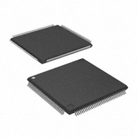


 工商网监
湘ICP备2023018690号
工商网监
湘ICP备2023018690号
