SM72238
www.ti.com
SNVS694C – JANUARY 2011 – REVISED APRIL 2013
Micropower Voltage Regulator
Check for Samples: SM72238
FEATURES
DESCRIPTION
•
•
•
•
•
•
•
•
•
•
•
The SM72238 is a micropower voltage regulator with
very low quiescent current (75µA typ.) and very low
dropout voltage (typ. 40mV at light loads and 380mV
at 100mA). It is ideally suited for use in batterypowered systems. Furthermore, the quiescent current
of the SM72238 increases only slightly in dropout,
prolonging battery life.
1
2
Renewable Energy Grade
High-Accuracy Output Voltage
Ensured 100mA Output Current
Extremely Low Quiescent Current
Low Dropout Voltage
Extremely Tight Load and Line Regulation
Very Low Temperature Coefficient
Use as Regulator or Reference
Needs Minimum Capacitance for Stability
Current and Thermal Limiting
Stable With Low-ESR Output Capacitors
(10mΩ to 6Ω)
The SM72238 is available in the surface-mount DPak package.
Careful design of the SM72238 has minimized all
contributions to the error budget. This includes a tight
initial tolerance (.5% typ.), extremely good load and
line regulation (.05% typ.) and a very low output
voltage temperature coefficient, making the part
useful as a low-power voltage reference.
Block Diagram and Typical Applications
Figure 1. SM72238
1
2
Please be aware that an important notice concerning availability, standard warranty, and use in critical applications of
Texas Instruments semiconductor products and disclaimers thereto appears at the end of this data sheet.
All trademarks are the property of their respective owners.
PRODUCTION DATA information is current as of publication date.
Products conform to specifications per the terms of the Texas
Instruments standard warranty. Production processing does not
necessarily include testing of all parameters.
Copyright © 2011–2013, Texas Instruments Incorporated
�SM72238
SNVS694C – JANUARY 2011 – REVISED APRIL 2013
www.ti.com
Connection Diagrams
Front View
Figure 2. PFM Package
See Package Number NDP0003B
These devices have limited built-in ESD protection. The leads should be shorted together or the device placed in conductive foam
during storage or handling to prevent electrostatic damage to the MOS gates.
Absolute Maximum Ratings (1) (2)
−0.3 to +30V
Input Supply Voltage
Power Dissipation
Internally Limited
Junction Temperature (TJ)
+150°C
−65° to +150°C
Ambient Storage Temperature
Soldering Dwell Time, Temperature
Wave
4 seconds, 260°C
Infrared
10 seconds, 240°C
Vapor Phase
ESD Rating
(1)
(2)
(3)
Human Body Model
75 seconds, 219°C
(3)
2500V
Absolute Maximum Ratings are limits beyond which damage to the device may occur. Operating Ratings are conditions under which
operation of the device is ensured. Operating Ratings do not imply ensured performance limits. For ensured performance limits and
associated test conditions, see the Electrical Characteristics tables.
If Military/Aerospace specified devices are required, please contact the TI Sales Office/ Distributors for availability and specifications.
Human Body Model 1.5kΩ in series with 100pF.
Operating Ratings (1)
Maximum Input Supply Voltage
30V
Junction Temperature Range, (TJ) (2)
(1)
(2)
2
−40° to +125°C
Absolute Maximum Ratings are limits beyond which damage to the device may occur. Operating Ratings are conditions under which
operation of the device is ensured. Operating Ratings do not imply ensured performance limits. For ensured performance limits and
associated test conditions, see the Electrical Characteristics tables.
Junction-to-case thermal resistance for the PFM package is 5.4°C/W.
Submit Documentation Feedback
Copyright © 2011–2013, Texas Instruments Incorporated
Product Folder Links: SM72238
�SM72238
www.ti.com
SNVS694C – JANUARY 2011 – REVISED APRIL 2013
Electrical Characteristics (1)
Conditions (1)
Parameter
Typ
Tested Limit (2)
Design Limit (3)
3.0
3.030
V max
2.970
V min
Units
3V Versions
Output Voltage
TJ = 25°C
−25°C ≤ TJ ≤ 85°C
Output Voltage
3.0
Full Operating Temperature Range
3.0
100µA ≤ IL ≤ 100mA,
TJ ≤ TJMAX
3.0
TJ = 25°C
3.3
3.045
V max
2.955
V min
3.060
V max
2.940
V min
3.072
V max
2.928
V min
3.3V Versions
Output Voltage
3.333
V max
3.267
Output Voltage
−25°C ≤ TJ ≤ 85°C
3.3
Full Operating Temperature Range
3.3
100µA ≤ IL ≤ 100mA
TJ ≤ TJMAX
3.3
TJ = 25°C
5.0
V min
3.350
V max
3.251
V min
3.366
V max
3.234
V min
3.379
V max
3.221
V min
5.0V Versions
Output Voltage
5.05
V max
4.95
−25°C ≤ TJ ≤ 85°C
5.0
Full Operating Temperature Range
5.0
100µA ≤ IL ≤ 100mA
TJ ≤ TJMAX
5.0
Output Voltage
Temperature Coefficient
See (4)
50
Line Regulation (5)
(VONOM + 1)V ≤ Vin ≤ 30V (6)
Output Voltage
V min
5.075
V max
4.925
V min
5.1
V max
4.9
V min
5.12
V max
4.88
V min
150
ppm/°C
All Voltage Options
0.04
0.2
% max
0.4
Load Regulation (5)
100µA ≤ IL ≤ 100mA
Dropout Voltage (7)
IL = 100µA
0.1
0.2
% max
0.3
80
50
IL = 100mA
(1)
(2)
(3)
(4)
(5)
(6)
(7)
% max
mV max
150
450
380
% max
mV max
mV max
600
mV max
Unless otherwise specified all limits ensured for VIN = (VONOM + 1)V, IL = 100µA and CL = 1µF. Limits appearing in boldface type apply
over the entire junction temperature range for operation. Limits appearing in normal type apply for TA = TJ = 25°C.
Ensured and 100% production tested.
Ensured but not 100% production tested. These limits are not used to calculate outgoing AQL levels.
Output or reference voltage temperature coefficient is defined as the worst case voltage change divided by the total temperature range.
Regulation is measured at constant junction temperature, using pulse testing with a low duty cycle. Changes in output voltage due to
heating effects are covered under the specification for thermal regulation.
For IL = 100µA and TJ = 125°C, line regulation is ensured by design to 0.2%. See Typical Performance Characteristics for line regulation
versus temperature and load current.
Dropout Voltage is defined as the input to output differential at which the output voltage drops 100 mV below its nominal value
measured at 1V differential. At very low values of programmed output voltage, the minimum input supply voltage of 2V (2.3V over
temperature) must be taken into account.
Submit Documentation Feedback
Copyright © 2011–2013, Texas Instruments Incorporated
Product Folder Links: SM72238
3
�SM72238
SNVS694C – JANUARY 2011 – REVISED APRIL 2013
www.ti.com
Electrical Characteristics(1) (continued)
Conditions (1)
Typ
Tested Limit (2)
IL = 100µA
75
120
IL = 100mA
8
12
Vin = (VONOM − 0.5)V,
IL = 100µA
110
170
Vout = 0
160
Parameter
Ground Current
Design Limit (3)
140
Current Limit
µA max
mA max
14
Dropout Ground Current
Units
µA max
mA max
µA max
200
200
µA max
mA max
220
mA max
Thermal Regulation
See (8)
0.05
Output Noise,
10 Hz to 100 kHz
CL = 1µF (5V Only)
430
µV rms
CL = 200µF
160
µV rms
CL = 3.3µF
(Bypass = 0.01µF)
100
µV rms
(8)
4
0.2
%/W
max
Thermal regulation is defined as the change in output voltage at a time T after a change in power dissipation is applied, excluding load
or line regulation effects. Specifications are for a 50mA load pulse at VIN = 30V (1.25W pulse) for T = 10ms.
Submit Documentation Feedback
Copyright © 2011–2013, Texas Instruments Incorporated
Product Folder Links: SM72238
�SM72238
www.ti.com
SNVS694C – JANUARY 2011 – REVISED APRIL 2013
Typical Performance Characteristics
Quiescent Current
Dropout Characteristics
Figure 3.
Figure 4.
Input Current
Input Current
Figure 5.
Figure 6.
Output Voltage
vs.
Temperature of 3
Representative Units
Quiescent Current
Figure 7.
Figure 8.
Submit Documentation Feedback
Copyright © 2011–2013, Texas Instruments Incorporated
Product Folder Links: SM72238
5
�SM72238
SNVS694C – JANUARY 2011 – REVISED APRIL 2013
www.ti.com
Typical Performance Characteristics (continued)
6
Quiescent Current
Quiescent Current
Figure 9.
Figure 10.
Quiescent Current
Short Circuit Current
Figure 11.
Figure 12.
Dropout Voltage
Line Transient Response
Figure 13.
Figure 14.
Submit Documentation Feedback
Copyright © 2011–2013, Texas Instruments Incorporated
Product Folder Links: SM72238
�SM72238
www.ti.com
SNVS694C – JANUARY 2011 – REVISED APRIL 2013
Typical Performance Characteristics (continued)
Load Transient Response
Load Transient Response
Figure 15.
Figure 16.
Output Impedance
Ripple Rejection
Figure 17.
Figure 18.
Ripple Rejection
Ripple Rejection
Figure 19.
Figure 20.
Submit Documentation Feedback
Copyright © 2011–2013, Texas Instruments Incorporated
Product Folder Links: SM72238
7
�SM72238
SNVS694C – JANUARY 2011 – REVISED APRIL 2013
www.ti.com
Typical Performance Characteristics (continued)
Shutdown Threshold Voltage
Line Regulation
Figure 21.
Figure 22.
Maximum Rated Output Current
Thermal Response
Figure 23.
Figure 24.
Output Capacitor ESR Range
Figure 25.
8
Submit Documentation Feedback
Copyright © 2011–2013, Texas Instruments Incorporated
Product Folder Links: SM72238
�SM72238
www.ti.com
SNVS694C – JANUARY 2011 – REVISED APRIL 2013
APPLICATION HINTS
EXTERNAL CAPACITORS
A 1.0µF (or greater) capacitor is required between the output and ground for stability. Without this capacitor the
part will oscillate. Most types of tantalum or aluminum electrolytics work fine here; even film types work but are
not recommended for reasons of cost. Many aluminum electrolytics have electrolytes that freeze at about −30°C,
so solid tantalums are recommended for operation below −25°C. The important parameters of the capacitor are
an ESR of about 5Ω or less and a resonant frequency above 500kHz. The value of this capacitor may be
increased without limit.
Ceramic capacitors whose value is greater than 1000pF should not be connected directly from the SM72238
output to ground. Ceramic capacitors typically have ESR values in the range of 5 to 10mΩ, a value below the
lower limit for stable operation (see Figure 25).
The reason for the lower ESR limit is that the loop compensation of the part relies on the ESR of the output
capacitor to provide the zero that gives added phase lead. The ESR of ceramic capacitors is so low that this
phase lead does not occur, significantly reducing phase margin. A ceramic output capacitor can be used if a
series resistance is added (recommended value of resistance about 0.1Ω to 2Ω).
At lower values of output current, less output capacitance is required for stability. The capacitor can be reduced
to 0.33µF for currents below 10mA or 0.1µF for currents below 1mA.
Unlike many other regulators, the SM72238 will remain stable and in regulation with no load in addition to the
internal voltage divider. This is especially important in CMOS RAM keep-alive applications.
A 1µF tantalum, ceramic or aluminum electrolytic capacitor should be placed from the SM72238 input to ground
if there is more than 10 inches of wire between the input and the AC filter capacitor or if a battery is used as the
input.
REDUCING OUTPUT NOISE
In reference applications it may be advantageous to reduce the AC noise present at the output. One method is to
reduce the regulator bandwidth by increasing the size of the output capacitor. This is the only way noise can be
reduced but is relatively inefficient, as increasing the capacitor from 1µF to 220µF only decreases the noise from
430µV to 160µV rms for a 100kHz bandwidth at 5V output.
Typical Applications
SM72238
*Minimum input-output voltage ranges from 40mV to 400mV, depending on load current. Current limit is typically
160mA.
Figure 26. 5 Volt Current Limiter
Submit Documentation Feedback
Copyright © 2011–2013, Texas Instruments Incorporated
Product Folder Links: SM72238
9
�SM72238
SNVS694C – JANUARY 2011 – REVISED APRIL 2013
www.ti.com
Schematic Diagram
10
Submit Documentation Feedback
Copyright © 2011–2013, Texas Instruments Incorporated
Product Folder Links: SM72238
�SM72238
www.ti.com
SNVS694C – JANUARY 2011 – REVISED APRIL 2013
REVISION HISTORY
Changes from Revision B (April 2013) to Revision C
•
Page
Changed layout of National Data Sheet to TI format .......................................................................................................... 10
Submit Documentation Feedback
Copyright © 2011–2013, Texas Instruments Incorporated
Product Folder Links: SM72238
11
�PACKAGE OPTION ADDENDUM
www.ti.com
3-Mar-2021
PACKAGING INFORMATION
Orderable Device
Status
(1)
Package Type Package Pins Package
Drawing
Qty
Eco Plan
(2)
Lead finish/
Ball material
MSL Peak Temp
Op Temp (°C)
Device Marking
(3)
(4/5)
(6)
SM72238TD-3.3/NOPB
ACTIVE
TO-252
NDP
3
75
RoHS & Green
SN
Level-2-260C-1 YEAR
-40 to 125
S72238
-3.3
SM72238TD-5.0/NOPB
ACTIVE
TO-252
NDP
3
75
RoHS & Green
SN
Level-2-260C-1 YEAR
-40 to 125
S72238
SM72238TDE-3.3/NOPB
NRND
TO-252
NDP
3
250
RoHS & Green
SN
Level-2-260C-1 YEAR
-40 to 125
S72238
-3.3
SM72238TDE-5.0/NOPB
NRND
TO-252
NDP
3
250
RoHS & Green
SN
Level-2-260C-1 YEAR
-40 to 125
S72238
SM72238TDX-3.3/NOPB
NRND
TO-252
NDP
3
2500
RoHS & Green
SN
Level-2-260C-1 YEAR
-40 to 125
S72238
-3.3
SM72238TDX-5.0/NOPB
NRND
TO-252
NDP
3
2500
RoHS & Green
SN
Level-2-260C-1 YEAR
-40 to 125
S72238
(1)
The marketing status values are defined as follows:
ACTIVE: Product device recommended for new designs.
LIFEBUY: TI has announced that the device will be discontinued, and a lifetime-buy period is in effect.
NRND: Not recommended for new designs. Device is in production to support existing customers, but TI does not recommend using this part in a new design.
PREVIEW: Device has been announced but is not in production. Samples may or may not be available.
OBSOLETE: TI has discontinued the production of the device.
(2)
RoHS: TI defines "RoHS" to mean semiconductor products that are compliant with the current EU RoHS requirements for all 10 RoHS substances, including the requirement that RoHS substance
do not exceed 0.1% by weight in homogeneous materials. Where designed to be soldered at high temperatures, "RoHS" products are suitable for use in specified lead-free processes. TI may
reference these types of products as "Pb-Free".
RoHS Exempt: TI defines "RoHS Exempt" to mean products that contain lead but are compliant with EU RoHS pursuant to a specific EU RoHS exemption.
Green: TI defines "Green" to mean the content of Chlorine (Cl) and Bromine (Br) based flame retardants meet JS709B low halogen requirements of
很抱歉,暂时无法提供与“SM72238TD-3.0/NOPB”相匹配的价格&库存,您可以联系我们找货
免费人工找货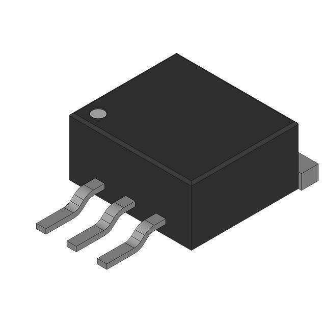


 工商网监
湘ICP备2023018690号
工商网监
湘ICP备2023018690号
