Sample &
Buy
Product
Folder
Support &
Community
Tools &
Software
Technical
Documents
SM74101
SNOSBA2B – JULY 2011 – REVISED MAY 2015
SM74101 Tiny 7A MOSFET Gate Driver
1 Features
3 Description
•
•
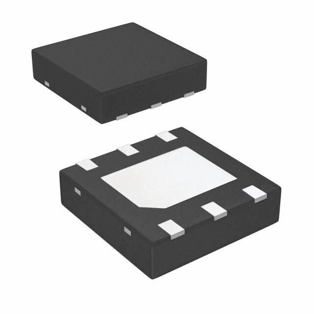
The SM74101 MOSFET gate driver provides high
peak gate drive current in the tiny WSON-6 package
(SOT23 equivalent footprint), with improved power
dissipation required for high frequency operation. The
compound output driver stage includes MOS and
bipolar transistors operating in parallel that together
sink more than 7A peak from capacitive loads.
Combining the unique characteristics of MOS and
bipolar devices reduces drive current variation with
voltage and temperature. Under-voltage lockout
protection is provided to prevent damage to the
MOSFET due to insufficient gate turn-on voltage. The
SM74101 provides both inverting and non-inverting
inputs to satisfy requirements for inverting and noninverting gate drive with a single device type.
1
•
•
•
•
•
•
•
•
Renewable Energy Grade
Compound CMOS and Bipolar Outputs Reduce
Output Current Variation
7A sink/3A Source Current
Fast Propagation Times (25 ns Typical)
Fast Rise and Fall Times (14 ns/12 ns Rise/Fall
with 2 nF Load)
Inverting and Non-Inverting Inputs Provide Either
Configuration with a Single Device
Supply Rail Under-Voltage Lockout Protection
Dedicated Input Ground (IN_REF) for Split Supply
or Single Supply Operation
Power Enhanced 6-Pin WSON Package (3.0mm x
3.0mm)
Output Swings from VCC to VEE which can be
Negative Relative to Input Ground
Device Information(1)
PACKAGE
BODY SIZE (NOM)
SM74101
WSON (6)
3.0 mm x 3.0 mm
(1) For all available packages, see the orderable addendum at
the end of the data sheet.
2 Applications
•
•
•
•
PART NUMBER
Solar Microinverter
AC/DC Switch-mode Power Supply
DC/DC Switch-mode Power Supply
Solenoid and Motor Drivers
VOUT
VIN
+10V
+5V
VCC
VCC
LM5110-1
UVLO
OUT
LM5025
CONTROLLER
IN_REF
IN_REF
IN
INB
OUT_B
OUT_B
IN_REF
IN_REF
FB
VEE
INB
OUT_A
IN_A
OUT_A
VEE
VEE
SM74101
-3V
Dual Supply
utilizing negative
Output voltage
Drive
SM74101 in a DC/DC Forward Topology Power Supply
1
An IMPORTANT NOTICE at the end of this data sheet addresses availability, warranty, changes, use in safety-critical applications,
intellectual property matters and other important disclaimers. PRODUCTION DATA.
�SM74101
SNOSBA2B – JULY 2011 – REVISED MAY 2015
www.ti.com
Table of Contents
1
2
3
4
5
6
7
Features ..................................................................
Applications ...........................................................
Description .............................................................
Revision History.....................................................
Pin Configuration and Functions .........................
Specifications.........................................................
1
1
1
2
3
4
6.1
6.2
6.3
6.4
6.5
6.6
6.7
4
4
4
4
4
5
6
Absolute Maximum Ratings ......................................
ESD Ratings..............................................................
Recommended Operating Conditions.......................
Thermal Information ..................................................
Electrical Characteristics...........................................
Switching Characteristics ..........................................
Typical Characteristics ..............................................
7.3 Feature Description................................................... 8
7.4 Device Functional Modes.......................................... 9
7.5 Thermal Considerations .......................................... 10
8
Application and Implementation ........................ 12
8.1 Application Information............................................ 12
8.2 Typical Application ................................................. 12
9 Power Supply Recommendations...................... 14
10 Layout................................................................... 14
10.1 Layout Guidelines ................................................. 14
10.2 Layout Example .................................................... 14
11 Device and Documentation Support ................. 16
Detailed Description .............................................. 8
11.1 Trademarks ........................................................... 16
11.2 Electrostatic Discharge Caution ............................ 16
11.3 Glossary ................................................................ 16
7.1 Overview ................................................................... 8
7.2 Functional Block Diagram ......................................... 8
12 Mechanical, Packaging, and Orderable
Information ........................................................... 17
4 Revision History
NOTE: Page numbers for previous revisions may differ from page numbers in the current version.
Changes from Revision A (April 2013) to Revision B
•
Added ESD Ratings table, Thermal Information table, Feature Description section, Device Functional Modes,
Application and Implementation section, Power Supply Recommendations section, Layout section, Device and
Documentation Support section, and Mechanical, Packaging, and Orderable Information section ..................................... 1
Changes from Original (April 2013) to Revision A
•
2
Page
Page
Changed layout of National Data Sheet to TI format ........................................................................................................... 11
Submit Documentation Feedback
Copyright © 2011–2015, Texas Instruments Incorporated
Product Folder Links: SM74101
�SM74101
www.ti.com
SNOSBA2B – JULY 2011 – REVISED MAY 2015
5 Pin Configuration and Functions
WSON
6-Pin
Top View
IN
VEE
VCC
1
6
2
5
3
4
INB
IN_REF
OUT
Pin Functions
PIN
I/O
DESCRIPTION
NAME
NO.
IN
1
I
TTL compatible thresholds. Pull up to VCC when not used.
VEE
2
-
Connect to either power ground or a negative gate drive supply for positive or negative
voltage swing.
VCC
3
I
Locally decouple to VEE. The decoupling capacitor should be located close to the chip.
OUT
4
O
Capable of sourcing 3A and sinking 7A. Voltage swing of this output is from VEE to VCC.
IN_REF
5
-
Connect to power ground (VEE) for standard positive only output voltage swing. Connect to
system logic ground when VEE is connected to a negative gate drive supply.
INB
6
I
TTL compatible thresholds. Connect to IN_REF when not used.
---
Exposed Pad
-
Internally bonded to the die substrate. Connect to VEE ground pin for low thermal
impedance.
Submit Documentation Feedback
Copyright © 2011–2015, Texas Instruments Incorporated
Product Folder Links: SM74101
3
�SM74101
SNOSBA2B – JULY 2011 – REVISED MAY 2015
www.ti.com
6 Specifications
6.1 Absolute Maximum Ratings
over operating free-air temperature range (unless otherwise noted)
(1)
MIN
MAX
UNIT
VCC to VEE
−0.3
15
V
VCC to IN_REF
−0.3
15
V
IN/INB to IN_REF
−0.3
15
V
IN_REF to VEE
−0.3
5
V
Tstg Storage temperature
−55
150
°C
150
°C
Maximum Junction Temperature
(1)
Stresses beyond those listed under Absolute Maximum Ratings may cause permanent damage to the device. These are stress ratings
only, which do not imply functional operation of the device at these or any other conditions beyond those indicated under Recommended
Operating Conditions. Exposure to absolute-maximum-rated conditions for extended periods may affect device reliability.
6.2 ESD Ratings
V(ESD)
(1)
Electrostatic discharge
VALUE
UNIT
±2000
V
Human-body model (HBM), per ANSI/ESDA/JEDEC JS-001 (1)
JEDEC document JEP155 states that 500-V HBM allows safe manufacturing with a standard ESD control process.
6.3 Recommended Operating Conditions
over operating free-air temperature range (unless otherwise noted)
Operating Junction Temperature
VCC Operating Range
VCC – IN_REF and VCC - VEE
MIN
MAX
UNIT
-40
125
°C
3.5
14
V
6.4 Thermal Information
SM74101
THERMAL METRIC
(1)
NGG
UNIT
6 PINS
RθJA
Junction-to-ambient thermal resistance, 0 LFPM Air Flow
40.0
RθJC(top)
Junction-to-case (top) thermal resistance
50.8
RθJB
Junction-to-board thermal resistance
29.3
ψJT
Junction-to-top characterization parameter
0.7
ψJB
Junction-to-board characterization parameter
29.5
RθJC(bot)
Junction-to-case (bottom) thermal resistance
7.5
(1)
°C/W
For more information about traditional and new thermal metrics, see the IC Package Thermal Metrics application report, SPRA953.
6.5 Electrical Characteristics
Over operating junction temperature range, VCC = 12 V, INB = IN_REF = VEE = 0V, No Load on output, unless otherwise
specified.
PARAMETER
TEST CONDITION
MIN
VCC – IN_REF
2.4
TYP
MAX
3.0
3.5
UNIT
SUPPLY
UVLO
VCC Under-voltage Lockout (rising)
VCCH
VCC Under-voltage Hysteresis
230
ICC
VCC Supply Current
1.0
V
mV
2.0
mA
CONTROL INPUTS
VIH
Logic High
VIL
Logic Low
VthH
High Threshold
4
2.3
1.3
Submit Documentation Feedback
V
1.75
0.8
V
2.3
V
Copyright © 2011–2015, Texas Instruments Incorporated
Product Folder Links: SM74101
�SM74101
www.ti.com
SNOSBA2B – JULY 2011 – REVISED MAY 2015
Electrical Characteristics (continued)
Over operating junction temperature range, VCC = 12 V, INB = IN_REF = VEE = 0V, No Load on output, unless otherwise
specified.
PARAMETER
TEST CONDITION
MIN
TYP
MAX
UNIT
0.8
1.35
2.0
V
VthL
Low Threshold
HYS
Input Hysteresis
IIL
Input Current Low
IN = INB = 0V
-1
0.1
1
µA
IIH
Input Current High
IN = INB = VCC
-1
0.1
1
µA
30
50
Ω
1.4
2.5
Ω
400
mV
OUTPUT DRIVER
ROH
Output Resistance High
IOUT = -10mA
(1)
(1)
ROL
Output Resistance Low
IOUT = 10mA
ISOURCE
Peak Source Current
OUT = VCC/2, 200ns pulsed current
3
A
ISINK
Peak Sink Current
OUT = VCC/2, 200ns pulsed current
7
A
500
mA
LATCHUP PROTECTION
AEC–Q100, METHOD 004
(1)
TJ = 150°C
The output resistance specification applies to the MOS device only. The total output current capability is the sum of the MOS and
Bipolar devices.
6.6 Switching Characteristics
over operating free-air temperature range (unless otherwise noted)
PARAMETER
TEST CONDITIONS
MIN
TYP
MAX
UNIT
td1
Propagation Delay Time Low to
High,
IN/ INB rising ( IN to OUT)
CLOAD = 2 nF, see Figure 11 and Figure 12
25
40
ns
td2
Propagation Delay Time High to
Low,
IN / INB falling (IN to OUT)
CLOAD = 2 nF, see Figure 11 and Figure 12
25
40
ns
tr
Rise time
CLOAD = 2 nF , see Figure 11 and Figure 12
14
ns
tf
Fall time
CLOAD = 2 nF , see Figure 11 and Figure 12
12
ns
Submit Documentation Feedback
Copyright © 2011–2015, Texas Instruments Incorporated
Product Folder Links: SM74101
5
�SM74101
SNOSBA2B – JULY 2011 – REVISED MAY 2015
www.ti.com
6.7 Typical Characteristics
100
100
VCC = 15V
SUPPLY CURRENT (mA)
SUPPLY CURRENT (mA)
f = 500kHz
10
VCC = 10V
1
VCC = 5V
10
f = 100kHz
1
f = 10kHz
TA = 25°C
TA = 25°C
VCC = 12V
CL = 2200pF
0.1
0.1
1
10
100
1000
CAPACITIVE LOAD (pF)
Figure 1. Supply Current vs Frequency
Figure 2. Supply Current vs Capacitive Load
20
18
TA = 25°C
VCC = 12V
CL = 2200pF
18
tr
16
14
tr
CL = 2200pF
16
TIME (ns)
TIME (ns)
10k
1k
100
FREQUENCY (kHz)
14
tf
12
tf
12
10
10
5 6
4
7
8
8
9 10 11 12 13 14 15 16
-75 -50 -25 0
SUPPLY VOLTAGE (V)
Figure 3. Rise and Fall Time vs Supply Voltage
Figure 4. Rise and Fall Time vs Temperature
32.5
50
TA = 25°C
40
25 50 75 100 125 150 175
TEMPERATURE (°C)
30
VCC = 12V
tD2
TIME (ns)
TIME (ns)
27.5
30
tr
20
25
tD1
22.5
tf
10
TA = 25°C
20
CL = 2200pF
17.5
0
100
1k
10k
CAPACITIVE LOAD (pF)
6
8
10
12
14
16
SUPPLY VOLTAGE (V)
Figure 5. Rise and Fall Time vs Capacitive Load
6
4
Submit Documentation Feedback
Figure 6. Delay Time vs Supply Voltage
Copyright © 2011–2015, Texas Instruments Incorporated
Product Folder Links: SM74101
�SM74101
www.ti.com
SNOSBA2B – JULY 2011 – REVISED MAY 2015
Typical Characteristics (continued)
3.25
35
65
VCC = 12V
32.5
TA = 25°C
CL = 2200pF
IOUT = 10mA
2.75
tD2
55
25
tD1
45
2.25
ROH
1.75
35
ROH (:)
27.5
ROL (:)
TIME (ns)
30
22.5
1.25
17.5
-75 -50 -25 0
15
0.75
25 50 75 100 125 150 175
3
0
TEMPERATURE (°C)
SINK
0.270
CURRENT (A)
0.330
Hysteresis
5
4
SOURCE
3
2
0.210
2.0
18
6
HYSTERESIS (V)
UVLO THRESHOLDS (V)
VCC - falling
2.3
15
7
0.390
2.6
12
8
VCC - rising
2.9
9
Figure 8. RDSON vs Supply Voltage
0.450
3.2
6
SUPPLY VOLTAGE (V)
Figure 7. Delay Time vs Temperature
TA = 25°C
1
1.7
-75 -50 -25 0
25
ROL
20
VOUT = 5V
0
0.150
25 50 75 100 125 150 175
5
7
9
11
13
15
SUPPLY VOLTAGE (V)
TEMPERATURE (°C)
Figure 9. UVLO Thresholds and Hysteresis vs Temperature
Figure 10. Peak Current vs Supply Voltage
Submit Documentation Feedback
Copyright © 2011–2015, Texas Instruments Incorporated
Product Folder Links: SM74101
7
�SM74101
SNOSBA2B – JULY 2011 – REVISED MAY 2015
www.ti.com
7 Detailed Description
7.1 Overview
The SM74101 is a high speed, high peak current (7A) single channel MOSFET driver. The high peak output
current of the SM74101 will switch power MOSFET’s on and off with short rise and fall times, thereby reducing
switching losses considerably. The SM74101 includes both inverting and non-inverting inputs that give the user
flexibility to drive the MOSFET with either active low or active high logic signals. The driver output stage consists
of a compound structure with MOS and bipolar transistor operating in parallel to optimize current capability over a
wide output voltage and operating temperature range. The bipolar device provides high peak current at the
critical Miller plateau region of the MOSFET VGS , while the MOS device provides rail-to-rail output swing. The
totem pole output drives the MOSFET gate between the gate drive supply voltage VCC and the power ground
potential at the VEE pin.
7.2 Functional Block Diagram
VCC
UVLO
IN
Level
Shift
OUT
INB
VEE
IN_REF
7.3 Feature Description
7.3.1 Detailed Operating Description
The control inputs of the driver are high impedance CMOS buffers with TTL compatible threshold voltages. The
negative supply of the input buffer is connected to the input ground pin IN_REF. An internal level shifting circuit
connects the logic input buffers to the totem pole output drivers. The level shift circuit and the separate
input/output ground pins provide the option of single supply or split supply configurations. When driving the
MOSFET gate from a single positive supply, the IN_REF and VEE pins are both connected to the power ground.
The isolated input and output stage grounds provide the capability to drive the MOSFET to a negative VGS
voltage for a more robust and reliable off state. In split supply configuration, the IN_REF pin is connected to the
ground of the controller which drives the SM74101 inputs. The VEE pin is connected to a negative bias supply
that can range from the IN_REF potential to as low as 14 V below the Vcc gate drive supply. For reliable
operation, the maximum voltage difference between VCC and IN_REF or between VCC and VEE is 14V.
The minimum recommended operating voltage between Vcc and IN_REF is 3.5V. An Under Voltage Lock Out
(UVLO) circuit is included in the SM74101 which senses the voltage difference between VCC and the input
ground pin, IN_REF. When the VCC to IN_REF voltage difference falls below 2.8V the driver is disabled and the
output pin is held in the low state. The UVLO hysteresis prevents chattering during brown-out conditions; the
driver will resume normal operation when the VCC to IN_REF differential voltage exceeds 3.0V.
8
Submit Documentation Feedback
Copyright © 2011–2015, Texas Instruments Incorporated
Product Folder Links: SM74101
�SM74101
www.ti.com
SNOSBA2B – JULY 2011 – REVISED MAY 2015
7.4 Device Functional Modes
7.4.1 Inverting Mode of Operation
During the inverting mode of operation, INB is used as the control input and the polarity of OUT is reversed with
respect to INB. A timing diagram of this mode is shown in Figure 11. The IN pin is not used in this mode of
operation and should be pulled up to VCC.
50%
50%
INB
tD2
tD1
OUTPUT
90%
10%
tr
tf
Figure 11. Inverting
7.4.2 Non-inverting Mode of Operation
During the non-inverting mode of operation, IN is used as the control input and the polarity of OUT is the same
with respect to IN. A timing diagram of this mode is shown in Figure 12. The INB pin is not used in this mode of
operation and should be connected to IN_REF.
50%
50%
IN
tD1
tD2
90%
OUTPUT
10%
tr
tf
Figure 12. Non-Inverting
Submit Documentation Feedback
Copyright © 2011–2015, Texas Instruments Incorporated
Product Folder Links: SM74101
9
�SM74101
SNOSBA2B – JULY 2011 – REVISED MAY 2015
www.ti.com
7.5 Thermal Considerations
The primary goal of the thermal management is to maintain the integrated circuit (IC) junction temperature (Tj)
below a specified limit to ensure reliable long term operation. The maximum TJ of IC components should be
estimated in worst case operating conditions. The junction temperature can be calculated based on the power
dissipated on the IC and the junction to ambient thermal resistance θJA for the IC package in the application
board and environment. The θJA is not a given constant for the package and depends on the PCB design and the
operating environment.
7.5.1 Drive Power Requirement Calculations In SM74101
SM74101 is a single low side MOSFET driver capable of sourcing / sinking 3A / 7A peak currents for short
intervals to drive a MOSFET without exceeding package power dissipation limits. High peak currents are
required to switch the MOSFET gate very quickly for operation at high frequencies.
VGATE
VHIGH
Q1
RG
VTRIG
CIN
Q2
Figure 13.
The schematic above shows a conceptual diagram of the SM74101 output and MOSFET load. Q1 and Q2 are
the switches within the gate driver. Rg is the gate resistance of the external MOSFET, and Cin is the equivalent
gate capacitance of the MOSFET. The equivalent gate capacitance is a difficult parameter to measure as it is the
combination of Cgs (gate to source capacitance) and Cgd (gate to drain capacitance). The Cgd is not a constant
and varies with the drain voltage. The better way of quantifying gate capacitance is the gate charge Qg in
coloumbs. Qg combines the charge required by Cgs and Cgd for a given gate drive voltage Vgate. The gate
resistance Rg is usually very small and losses in it can be neglected. The total power dissipated in the MOSFET
driver due to gate charge is approximated by:
PDRIVER = VGATE x QG x FSW
Where
•
FSW = switching frequency of the MOSFET.
(1)
For example, consider the MOSFET MTD6N15 whose gate charge specified as 30 nC for VGATE = 12V.
Therefore, the power dissipation in the driver due to charging and discharging of MOSFET gate capacitances at
switching frequency of 300 kHz and VGATE of 12V is equal to
PDRIVER = 12V x 30 nC x 300 kHz = 0.108W.
(2)
In addition to the above gate charge power dissipation, - transient power is dissipated in the driver during output
transitions. When either output of the SM74101 changes state, current will flow from VCC to VEE for a very brief
interval of time through the output totem-pole N and P channel MOSFETs. The final component of power
dissipation in the driver is the power associated with the quiescent bias current consumed by the driver input
stage and Under-voltage lockout sections.
Characterization of the SM74101 provides accurate estimates of the transient and quiescent power dissipation
components. At 300 kHz switching frequency and 30 nC load used in the example, the transient power will be 8
mW. The 1 mA nominal quiescent current and 12V VGATE supply produce a 12 mW typical quiescent power.
Therefore the total power dissipation
10
Submit Documentation Feedback
Copyright © 2011–2015, Texas Instruments Incorporated
Product Folder Links: SM74101
�SM74101
www.ti.com
SNOSBA2B – JULY 2011 – REVISED MAY 2015
Thermal Considerations (continued)
PD = 0.118 + 0.008 + 0.012 = 0.138W.
(3)
We know that the junction temperature is given by
TJ = PD x θJA + TA
(4)
Or the rise in temperature is given by
TRISE = TJ − TA = PD x θJA
(5)
For WSON-6 package, the integrated circuit die is attached to leadframe die pad which is soldered directly to the
printed circuit board. This substantially decreases the junction to ambient thermal resistance (θJA). By providing
suitable means of heat dispersion from the IC to the ambient through exposed copper pad, which can readily
dissipate heat to the surroundings, θJA as low as 40°C / Watt is achievable with the package. The resulting Trise
for the driver example above is thereby reduced to just 5.5 degrees.
Therefore TRISE is equal to
TRISE = 0.138 x 40 = 5.5°C
(6)
Submit Documentation Feedback
Copyright © 2011–2015, Texas Instruments Incorporated
Product Folder Links: SM74101
11
�SM74101
SNOSBA2B – JULY 2011 – REVISED MAY 2015
www.ti.com
8 Application and Implementation
NOTE
Information in the following applications sections is not part of the TI component
specification, and TI does not warrant its accuracy or completeness. TI’s customers are
responsible for determining suitability of components for their purposes. Customers should
validate and test their design implementation to confirm system functionality.
8.1 Application Information
The SM74101 can be used to drive a low side MOSFET with very low switching losses. Either one of the control
input pins, IN or INB, can be used to control the gate drive to the MOSFET. The choice of the control input pin
used will depend on the polarity of operation.
8.2 Typical Application
The SM74101 is utilized in a DC/DC forward topology power supply as shown in Figure 14. The high peak gate
drive current of the SM74101 allows for short rise and fall times on the primary side MOSFET, thereby improving
overall efficiency of the system and reducing switching losses. It is used in conjunction with the LM5025 Active
Clamp Voltage Mode PWM Controller to provide drive capability to the primary side MOSFET after isolation.
VOUT
VIN
+10V
+5V
VCC
VCC
LM5110-1
UVLO
OUT
LM5025
CONTROLLER
IN_REF
IN_REF
INB
OUT_B
IN
OUT_B
IN_REF
IN_REF
FB
VEE
INB
IN_A
OUT_A
OUT_A
VEE
VEE
SM74101
-3V
Dual Supply
utilizing negative
Output voltage
Drive
Figure 14. DC/DC Forward Topology Power Supply
8.2.1 Design Requirements
The SM74101 is used in the non-inverting mode of operation. The IN pin is used to control the OUT signal to the
primary side MOSFET. The signal that travels from OUT_A and through the isolation transformer should be
compatible with the high and low threshold voltages of the IN pin. INB is not used in this mode and is therefore
connected to IN_REF, which is also the primary side ground.
12
Submit Documentation Feedback
Copyright © 2011–2015, Texas Instruments Incorporated
Product Folder Links: SM74101
�SM74101
www.ti.com
SNOSBA2B – JULY 2011 – REVISED MAY 2015
Typical Application (continued)
8.2.2 Detailed Design Procedure
See Power Supply Recommendations, Layout, and Thermal Considerations for key design considerations
regarding the input supply, grounding, and thermal calculations specific to the SM74101.
8.2.3 Application Curve
The rise and fall times of the OUT signal will depend on the capacitance of the MOSFET gate. Therefore, an
appropriate MOSFET should be selected to meet the switching speed and efficiency requirements of the system.
50
TA = 25°C
TIME (ns)
40
VCC = 12V
30
tr
20
tf
10
0
100
1k
10k
CAPACITIVE LOAD (pF)
Figure 15. Rise and Fall Time vs Capacitive Load
Submit Documentation Feedback
Copyright © 2011–2015, Texas Instruments Incorporated
Product Folder Links: SM74101
13
�SM74101
SNOSBA2B – JULY 2011 – REVISED MAY 2015
www.ti.com
9 Power Supply Recommendations
A Low ESR/ESL capacitor must be connected close to the IC and between the VCC and VEE pins to support high
peak currents being drawn from VCC during turn-on of the MOSFET. Also, if either channel is not being used, the
respective input pin (IN or INB) should be connected to either VEE or VCC to avoid spurious output signals.
10 Layout
10.1 Layout Guidelines
Attention must be given to board layout when using the SM74101. Proper grounding is crucial. The driver needs
a very low impedance path for current return to ground avoiding inductive loops. Two paths for returning current
to ground are a) between SM74101 IN_REF pin and the ground of the circuit that controls the driver inputs and
b) between SM74101 VEE pin and the source of the power MOSFET being driven. Both paths should be as short
as possible to reduce inductance and be as wide as possible to reduce resistance. These ground paths should
be distinctly separate to avoid coupling between the high current paths (VCC, VEE, and OUT) and the logic
signal paths (IN, INB, and IN_REF) of the SM74101. With rise and fall times in the range of 10 to 30 ns, care is
required to minimize the lengths of current carrying conductors to reduce their inductance and EMI from the high
di/dt transients generated when driving large capacitive loads.
10.2 Layout Example
Figure 16 shows an example layout for the SM74101 configured in the non-inverting mode of operation. In this
mode, the INB pin is not used and is connected to IN_REF. Two low ESR/ESL capacitors, C1 and C2, are used
for input decoupling purposes and are placed as close as possible to the IC.
The level shift circuit and the separate input/output ground pins provide the option of single supply or split supply
configurations. When driving the MOSFET gate from a single positive supply, the control ground should be
connected to the power ground in an area of the board where the least amount of noise will exist. Otherwise,
when using a split supply configuration, the control ground and power ground paths should be distinctly separate
to avoid noise coupling between the two paths.
14
Submit Documentation Feedback
Copyright © 2011–2015, Texas Instruments Incorporated
Product Folder Links: SM74101
�SM74101
www.ti.com
SNOSBA2B – JULY 2011 – REVISED MAY 2015
Layout Example (continued)
Figure 16. SM74101 Layout Example
Submit Documentation Feedback
Copyright © 2011–2015, Texas Instruments Incorporated
Product Folder Links: SM74101
15
�SM74101
SNOSBA2B – JULY 2011 – REVISED MAY 2015
www.ti.com
11 Device and Documentation Support
11.1 Trademarks
All trademarks are the property of their respective owners.
11.2 Electrostatic Discharge Caution
These devices have limited built-in ESD protection. The leads should be shorted together or the device placed in conductive foam
during storage or handling to prevent electrostatic damage to the MOS gates.
11.3 Glossary
SLYZ022 — TI Glossary.
This glossary lists and explains terms, acronyms, and definitions.
16
Submit Documentation Feedback
Copyright © 2011–2015, Texas Instruments Incorporated
Product Folder Links: SM74101
�SM74101
www.ti.com
SNOSBA2B – JULY 2011 – REVISED MAY 2015
12 Mechanical, Packaging, and Orderable Information
The following pages include mechanical, packaging, and orderable information. This information is the most
current data available for the designated devices. This data is subject to change without notice and revision of
this document. For browser-based versions of this data sheet, refer to the left-hand navigation.
Submit Documentation Feedback
Copyright © 2011–2015, Texas Instruments Incorporated
Product Folder Links: SM74101
17
�PACKAGE OPTION ADDENDUM
www.ti.com
10-Dec-2020
PACKAGING INFORMATION
Orderable Device
Status
(1)
Package Type Package Pins Package
Drawing
Qty
Eco Plan
(2)
Lead finish/
Ball material
MSL Peak Temp
Op Temp (°C)
Device Marking
(3)
(4/5)
(6)
SM74101SD/NOPB
ACTIVE
WSON
NGG
6
1000
RoHS & Green
SN
Level-1-260C-UNLIM
-40 to 125
L264B
SM74101SDX/NOPB
ACTIVE
WSON
NGG
6
4500
RoHS & Green
SN
Level-1-260C-UNLIM
-40 to 125
L264B
(1)
The marketing status values are defined as follows:
ACTIVE: Product device recommended for new designs.
LIFEBUY: TI has announced that the device will be discontinued, and a lifetime-buy period is in effect.
NRND: Not recommended for new designs. Device is in production to support existing customers, but TI does not recommend using this part in a new design.
PREVIEW: Device has been announced but is not in production. Samples may or may not be available.
OBSOLETE: TI has discontinued the production of the device.
(2)
RoHS: TI defines "RoHS" to mean semiconductor products that are compliant with the current EU RoHS requirements for all 10 RoHS substances, including the requirement that RoHS substance
do not exceed 0.1% by weight in homogeneous materials. Where designed to be soldered at high temperatures, "RoHS" products are suitable for use in specified lead-free processes. TI may
reference these types of products as "Pb-Free".
RoHS Exempt: TI defines "RoHS Exempt" to mean products that contain lead but are compliant with EU RoHS pursuant to a specific EU RoHS exemption.
Green: TI defines "Green" to mean the content of Chlorine (Cl) and Bromine (Br) based flame retardants meet JS709B low halogen requirements of