��������� �������
������� ��������� �������
� ��
��
�� ��� ��
������
���� �������
The SN5405 is obsolete
and no longer is supplied.
SDLS030A − DECEMBER 1983 − REVISED NOVEMBER 2003
D Package Options Include Plastic
D Dependable Texas Instrument Quality and
Reliability
1A
1Y
2A
2Y
3A
3Y
GND
1
14
2
13
3
12
4
11
5
10
6
9
7
8
VCC
6A
6Y
5A
5Y
4A
4Y
1A
2Y
2A
1
14
2
13
3
12
VCC
3A
3Y
4A
4
11
5
10
6
9
7
8
1Y
6A
6Y
GND
5Y
5A
4Y
SN54LS05, SN54S05 . . . FK PACKAGE
(TOP VIEW)
1Y
1A
NC
VCC
6A
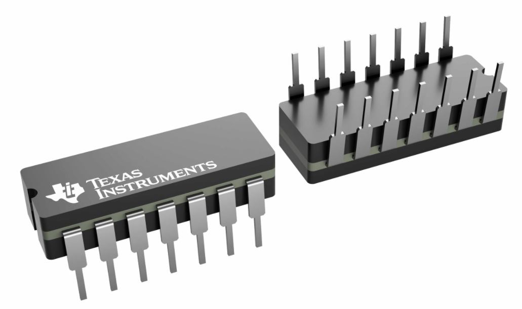
SN5405, SN54LS05, SN54S05 . . . J PACKAGE
SN7405 . . . N PACKAGE
SN74LS05 . . . D, DB, N, OR NS PACKAGE
SN74S05 . . . D, N, OR NS PACKAGE
SN54LS05, SN54S05 . . . W PACKAGE
(TOP VIEW)
(TOP VIEW)
2A
NC
2Y
NC
3A
4
3 2 1 20 19
18
5
17
6
16
7
15
8
14
9 10 11 12 13
6Y
NC
5A
NC
5Y
3Y
GND
NC
4Y
4A
Small-Outline (D, NS), Shrink Small-Outline
(DB), and Ceramic Flat (W) Packages,
Ceramic Chip Carriers (FK), and Standard
Plastic (N) and Ceramic (J) DIPs
NC − No internal connection
description/ordering information
These devices contain six independent inverters. To perform correctly, the open-collector outputs require pullup
resistors. These devices may be connected to other open-collector outputs to implement active-low wired-OR
or active-high wire-AND functions. Open-collector devices often are used to generate high VOH levels.
ORDERING INFORMATION
PDIP − N
0°C to 70°C
−55°C to 125°C
ORDERABLE
PART NUMBER
PACKAGE†
TA
SOIC − D
Tube
SN7405N
SN74LS05N
SN74LS05N
SN74S05N
SN74S05N
SN74LS05D
Tape and reel
SN74LS05DR
Tube
SN74S05D
Tape and reel
SN74S05DR
Tape and reel
SSOP − DB
Tape and reel
CDIP − J
Tube
CDIP − W
Tube
LCCC − FK
SN7405N
Tube
SOP − NS
Tube
TOP-SIDE
MARKING
LS05
S05
SN74LS05NSR
74LS05
SN74S05NSR
74S05
SN74LS05DBR
LS05
SNJ54LS05J
SNJ54LS05J
SNJ54S05J
SNJ54S05J
SNJ54LS05W
SNJ54LS05W
SNJ54S05W
SNJ54S05W
SNJ54LS05FK
SNJ54LS05FK
SNJ54S05FK
SNJ54S05FK
† Package drawings, standard packing quantities, thermal data, symbolization, and PCB design
guidelines are available at www.ti.com/sc/package.
Please be aware that an important notice concerning availability, standard warranty, and use in critical applications of
Texas Instruments semiconductor products and disclaimers thereto appears at the end of this data sheet.
Copyright 2003, Texas Instruments Incorporated
���������� ���� ����������� �! "#��$�� �! �� %#&'�"����� (��$)
���(#"�! "������ �� !%$"���"�����! %$� �*$ �$��! �� �$+�! ��!��#�$��!
!���(��( ,������-) ���(#"���� %��"$!!��. (�$! ��� �$"$!!���'- ��"'#($
�$!���. �� �'' %����$�$�!)
�� %��(#"�! "��%'���� �� /�����0�12�1�� �'' %����$�$�! ��$ �$!�$(
#�'$!! ��*$�,�!$ ���$() �� �'' ��*$� %��(#"�!� %��(#"����
%��"$!!��. (�$! ��� �$"$!!���'- ��"'#($ �$!���. �� �'' %����$�$�!)
POST OFFICE BOX 655303
• DALLAS, TEXAS 75265
1
���������� �������
������� ��������� �������
� ��
��
�� ��� ��
������
���� �������
The SN5405 is obsolete
and no longer is supplied.
SDLS030A − DECEMBER 1983 − REVISED NOVEMBER 2003
FUNCTION TABLE
(each inverter)
INPUT
A
OUTPUT
Y
H
L
L
H
logic diagram (positive logic)
1A
1
2
1Y
2A
3
4
2Y
3A
5
6
3Y
4A
9
8
4Y
5A
11
10
5Y
6A
13
12
6Y
Y=A
Pin numbers shown are for the D, DB, J, N, and NS packages.
2
POST OFFICE BOX 655303
• DALLAS, TEXAS 75265
���������� �������
������� ��������� �������
� ��
��
�� ��� ��
������
���� �������
The SN5405 is obsolete
and no longer is supplied.
SDLS030A − DECEMBER 1983 − REVISED NOVEMBER 2003
schematic (each inverter)
’05
’LS05
VCC
4 kΩ
VCC
1.6 kΩ
8 kΩ
20 kΩ
Input
A
Input
A
Output
Y
1 kΩ
Output
Y
4.5 kΩ
GND
GND
’S05
VCC
2.8 kΩ
900 Ω
Input
A
Output
Y
250 Ω
500 Ω
Resistor values shown are nominal.
absolute maximum ratings over operating free-air temperature (unless otherwise noted)†
Supply voltage, VCC (see Note 1): ’05, ’LS05, ’S05 . . . . . . . . . . . . . . . . . . . . . . . . . . . . . . . . . . . . . . . . . . . . . . 7 V
Input voltage, VI: ’05, ’S05 . . . . . . . . . . . . . . . . . . . . . . . . . . . . . . . . . . . . . . . . . . . . . . . . . . . . . . . . . . . . . . . . . 5.5 V
’LS05 . . . . . . . . . . . . . . . . . . . . . . . . . . . . . . . . . . . . . . . . . . . . . . . . . . . . . . . . . . . . . . . . . . . . . . 7 V
Off-state output voltage, VO . . . . . . . . . . . . . . . . . . . . . . . . . . . . . . . . . . . . . . . . . . . . . . . . . . . . . . . . . . . . . . . . . . 7 V
Package thermal impedance, θJA (see Note 2): D package . . . . . . . . . . . . . . . . . . . . . . . . . . . . . . . . . . . 86°C/W
DB package . . . . . . . . . . . . . . . . . . . . . . . . . . . . . . . . . 96°C/W
N package . . . . . . . . . . . . . . . . . . . . . . . . . . . . . . . . . . . 80°C/W
NS package . . . . . . . . . . . . . . . . . . . . . . . . . . . . . . . . . 76°C/W
Storage temperature range, Tstg . . . . . . . . . . . . . . . . . . . . . . . . . . . . . . . . . . . . . . . . . . . . . . . . . . . −65°C to 150°C
† Stresses beyond those listed under “absolute maximum ratings” may cause permanent damage to the device. These are stress ratings only, and
functional operation of the device at these or any other conditions beyond those indicated under “recommended operating conditions” is not
implied. Exposure to absolute-maximum-rated conditions for extended periods may affect device reliability.
NOTES: 1. Voltage values are with respect to network ground terminal.
2. The package thermal impedance is calculated in accordance with JESD 51-7.
POST OFFICE BOX 655303
• DALLAS, TEXAS 75265
3
���������� �������
������� ��������� �������
� ��
��
�� ��� ��
������
���� �������
The SN5405 is obsolete
and no longer is supplied.
SDLS030A − DECEMBER 1983 − REVISED NOVEMBER 2003
recommended operating conditions
SN5405
SN7405
MIN
NOM
MAX
MIN
NOM
MAX
4.5
5
5.5
4.75
5
5.25
UNIT
VCC
VIH
Supply voltage
VIL
VOH
Low-level input voltage
0.8
0.8
High-level output voltage
5.5
5.5
V
IOL
TA
Low-level output current
16
16
mA
70
°C
High-level input voltage
2
Operating free-air temperature
2
−55
125
V
V
0
V
electrical characteristics over recommended operating free-air temperature range (unless
otherwise noted)
TEST CONDITIONS†
PARAMETER
VIK
VCC = MIN,
MIN
SN5405
TYP‡
MAX
II = −12 mA
IOH
VCC = MIN,
VOH = 5.5 V
VOL
II
VCC = MIN,
VCC = MAX,
VIH = 2 V,
VI = 5.5 V
IIH
IIL
VCC = MAX,
VCC = MAX,
VI = 2.4 V
VI = 0.4 V
ICCH
ICCL
VCC = MAX,
VCC = MAX,
VI = 0 V
VI = 4.5 V
MIN
SN7405
TYP‡
−1.5
VIL = 0.8 V
VIL = 0.7 V
MAX
−1.5
UNIT
V
0.25
mA
0.25
IOL = 16 mA
0.2
0.4
0.2
0.4
V
1
1
mA
40
40
µA
−1.6
−1.6
mA
6
12
mA
18
33
18
† For conditions shown as MIN or MAX, use the appropriate value specified under recommended operating conditions.
‡ All typical values are at VCC = 5 V, TA = 25°C.
33
mA
6
12
switching characteristics, VCC = 5 V, TA = 25°C (see Figure 1)
PARAMETER
tPLH
tPHL
4
FROM
(INPUT)
TO
(OUTPUT)
A
Y
POST OFFICE BOX 655303
TEST CONDITIONS
RL = 4 kΩ
RL = 400 Ω
• DALLAS, TEXAS 75265
CL = 15 pF
MIN
TYP
MAX
40
55
8
15
UNIT
ns
���������� �������
������� ��������� �������
� ��
��
�� ��� ��
������
���� �������
The SN5405 is obsolete
and no longer is supplied.
SDLS030A − DECEMBER 1983 − REVISED NOVEMBER 2003
recommended operating conditions
SN54LS05
SN74LS05
MIN
NOM
MAX
MIN
NOM
MAX
4.5
5
5.5
4.75
5
5.25
UNIT
VCC
VIH
Supply voltage
VIL
VOH
Low-level input voltage
0.7
0.8
High-level output voltage
5.5
5.5
IOL
TA
Low-level output current
4
8
mA
70
°C
High-level input voltage
2
Operating free-air temperature
2
−55
125
V
V
0
V
V
electrical characteristics over recommended operating free-air temperature range (unless
otherwise noted)
SN54LS05
TYP‡
MAX
TEST CONDITIONS†
PARAMETER
VIK
IOH
VCC = MIN,
VCC = MIN,
II = −18 mA
VIL = MAX,
VOL
VCC = MIN,
VIH = 2 V
II
IIH
VCC = MAX,
VCC = MAX,
VI = 7 V
VI = 2.7 V
IIL
ICCH
VCC = MAX,
VCC = MAX,
VI = 0.4 V
VI = 0 V
MIN
VOH = 5.5 V
IOL = 4 mA
SN74LS05
TYP‡
MAX
MIN
UNIT
−1.5
−1.5
V
0.1
0.1
mA
0.25
0.4
IOL = 8 mA
0.25
0.4
0.35
0.5
V
0.1
0.1
mA
20
20
µA
−0.4
−0.4
mA
1.2
2.4
mA
ICCL
VCC = MAX,
VI = 4.5 V
3.6
6.6
3.6
† For conditions shown as MIN or MAX, use the appropriate value specified under recommended operating conditions.
‡ All typical values are at VCC = 5 V, TA = 25°C.
6.6
mA
1.2
2.4
switching characteristics, VCC = 5 V, TA = 25°C (see Figure 2)
PARAMETER
FROM
(INPUT)
TO
(OUTPUT)
tPLH
tPHL
A
Y
POST OFFICE BOX 655303
TEST CONDITIONS
RL = 2 kΩ,
CL = 15 pF
• DALLAS, TEXAS 75265
MIN
TYP
MAX
17
32
15
28
UNIT
ns
5
���������� �������
������� ��������� �������
� ��
��
�� ��� ��
������
���� �������
The SN5405 is obsolete
and no longer is supplied.
SDLS030A − DECEMBER 1983 − REVISED NOVEMBER 2003
recommended operating conditions
SN54S05
SN74S05
MIN
NOM
MAX
MIN
NOM
MAX
4.5
5
5.5
4.75
5
5.25
UNIT
VCC
VIH
Supply voltage
VIL
VOH
Low-level input voltage
0.8
0.8
High-level output voltage
5.5
5.5
V
IOL
TA
Low-level output current
20
20
mA
70
°C
High-level input voltage
2
Operating free-air temperature
2
−55
125
V
V
0
V
electrical characteristics over recommended operating free-air temperature range (unless
otherwise noted)
TEST CONDITIONS†
PARAMETER
VIK
VCC = MIN,
MIN
SN54S05
TYP‡
MAX
II = −18 mA
IOH
VCC = MIN,
VOH = 5.5 V
VOL
II
VCC = MIN,
VCC = MAX,
VIH = 2 V,
VI = 5.5 V
IIH
IIL
VCC = MAX,
VCC = MAX,
VI = 2.7 V
VI = 0.5 V
ICCH
ICCL
VCC = MAX,
VCC = MAX,
VI = 0 V
VI = 4.5 V
MIN
SN74S05
TYP‡
MAX
−1.2
VIL = 0.8 V
VIL = 0.7 V
−1.2
UNIT
V
0.25
mA
0.25
IOL = 20 mA
0.5
0.5
1
1
mA
50
50
µA
−2
V
−2
mA
9
19.8
mA
30
54
30
† For conditions shown as MIN or MAX, use the appropriate value specified under recommended operating conditions.
‡ All typical values are at VCC = 5 V, TA = 25°C.
54
mA
9
19.8
switching characteristics, VCC = 5 V, TA = 25°C (see Figure 1)
PARAMETER
tPLH
tPHL
tPLH
tPHL
6
FROM
(INPUT)
TO
(OUTPUT)
TEST CONDITIONS
CL = 15 pF
A
Y
RL = 280 Ω
• DALLAS, TEXAS 75265
TYP
MAX
2
5
7.5
2
4.5
7
UNIT
ns
7.5
CL = 50 pF
POST OFFICE BOX 655303
MIN
7
ns
���������� �������
������� ��������� �������
� ��
��
�� ��� ��
������
���� �������
The SN5405 is obsolete
and no longer is supplied.
SDLS030A − DECEMBER 1983 − REVISED NOVEMBER 2003
PARAMETER MEASUREMENT INFORMATION
SERIES 54/74 AND 54S/74S DEVICES
VCC
RL
From Output
Under Test
Test Point
CL
(see Note A)
LOAD CIRCUIT
3V
1.5 V
Input
1.5 V
0V
tPLH
High-Level
Pulse
1.5 V
VOH
In-Phase
Output
1.5 V
1.5 V
1.5 V
VOL
tPHL
tw
Low-Level
Pulse
tPHL
1.5 V
1.5 V
tPLH
VOH
Out-of-Phase
Output
1.5 V
1.5 V
VOL
VOLTAGE WAVEFORMS
PROPAGATION DELAY TIMES
VOLTAGE WAVEFORMS
PULSE WIDTHS
NOTES: A. CL includes probe and jig capacitance.
B. In the examples above, the phase relationships between inputs and outputs have been chosen arbitrarily.
C. All input pulses are supplied by generators having the following characteristics: PRR ≤ 1 MHz, ZO = 50 Ω, and:
For Series 54/74, tr ≤ 7 ns, tf ≤ 7 ns.
For Series 54S/74S, tr ≤ 2.5 ns, tf ≤ 2.5 ns.
D. The outputs are measured one at a time with one input transition per measurement.
Figure 1. Load Circuit and Voltage Waveforms
POST OFFICE BOX 655303
• DALLAS, TEXAS 75265
7
���������� �������
������� ��������� �������
� ��
��
�� ��� ��
������
���� �������
The SN5405 is obsolete
and no longer is supplied.
SDLS030A − DECEMBER 1983 − REVISED NOVEMBER 2003
PARAMETER MEASUREMENT INFORMATION
SERIES 54LS/74LS DEVICES
VCC
RL
From Output
Under Test
Test Point
CL
(see Note A)
LOAD CIRCUIT
3V
1.3 V
Input
1.3 V
0V
tPLH
High-Level
Pulse
1.3 V
1.3 V
1.3 V
1.3 V
tPLH
VOH
Out-of-Phase
Output
1.3 V
1.3 V
VOL
VOLTAGE WAVEFORMS
PROPAGATION DELAY TIMES
CL includes probe and jig capacitance.
In the examples above, the phase relationships between inputs and outputs have been chosen arbitrarily.
All input pulses are supplied by generators having the following characteristics: PRR ≤ 1 MHz, ZO = 50 Ω, tr ≤ 1.5 ns, tf ≤ 2.6 ns.
The outputs are measured one at a time with one input transition per measurement.
Figure 2. Load Circuit and Voltage Waveforms
8
1.3 V
VOL
tPHL
VOLTAGE WAVEFORMS
PULSE WIDTHS
NOTES: A.
B.
C.
D.
VOH
In-Phase
Output
1.3 V
tw
Low-Level
Pulse
tPHL
POST OFFICE BOX 655303
• DALLAS, TEXAS 75265
�PACKAGE OPTION ADDENDUM
www.ti.com
17-Jan-2023
PACKAGING INFORMATION
Orderable Device
Status
(1)
Package Type Package Pins Package
Drawing
Qty
Eco Plan
(2)
Lead finish/
Ball material
MSL Peak Temp
Op Temp (°C)
Device Marking
(3)
Samples
(4/5)
(6)
JM38510/07004BCA
ACTIVE
CDIP
J
14
1
Non-RoHS
& Green
SNPB
N / A for Pkg Type
-55 to 125
JM38510/
07004BCA
Samples
M38510/07004BCA
ACTIVE
CDIP
J
14
1
Non-RoHS
& Green
SNPB
N / A for Pkg Type
-55 to 125
JM38510/
07004BCA
Samples
SN54LS05J
ACTIVE
CDIP
J
14
1
Non-RoHS
& Green
SNPB
N / A for Pkg Type
-55 to 125
SN54LS05J
Samples
SN54S05J
ACTIVE
CDIP
J
14
1
Non-RoHS
& Green
SNPB
N / A for Pkg Type
-55 to 125
SN54S05J
Samples
SN7405N
ACTIVE
PDIP
N
14
25
RoHS & Green
NIPDAU
N / A for Pkg Type
0 to 70
SN7405N
Samples
SN7405NE4
ACTIVE
PDIP
N
14
25
RoHS & Green
NIPDAU
N / A for Pkg Type
0 to 70
SN7405N
Samples
SN74LS05D
ACTIVE
SOIC
D
14
50
RoHS & Green
NIPDAU
Level-1-260C-UNLIM
0 to 70
LS05
Samples
SN74LS05DBR
ACTIVE
SSOP
DB
14
2000
RoHS & Green
NIPDAU
Level-1-260C-UNLIM
0 to 70
LS05
Samples
SN74LS05DR
ACTIVE
SOIC
D
14
2500
RoHS & Green
NIPDAU
Level-1-260C-UNLIM
0 to 70
LS05
Samples
SN74LS05N
ACTIVE
PDIP
N
14
25
RoHS & Green
NIPDAU
N / A for Pkg Type
0 to 70
SN74LS05N
Samples
SN74LS05NE4
ACTIVE
PDIP
N
14
25
RoHS & Green
NIPDAU
N / A for Pkg Type
0 to 70
SN74LS05N
Samples
SN74LS05NSR
ACTIVE
SO
NS
14
2000
RoHS & Green
NIPDAU
Level-1-260C-UNLIM
0 to 70
74LS05
Samples
SN74S05D
ACTIVE
SOIC
D
14
50
RoHS & Green
NIPDAU
Level-1-260C-UNLIM
0 to 70
S05
Samples
SN74S05N
ACTIVE
PDIP
N
14
25
RoHS & Green
NIPDAU
N / A for Pkg Type
0 to 70
SN74S05N
Samples
SN74S05NSR
ACTIVE
SO
NS
14
2000
RoHS & Green
NIPDAU
Level-1-260C-UNLIM
0 to 70
74S05
Samples
SNJ54LS05FK
ACTIVE
LCCC
FK
20
1
Non-RoHS
& Green
SNPB
N / A for Pkg Type
-55 to 125
SNJ54LS
05FK
Samples
SNJ54LS05J
ACTIVE
CDIP
J
14
1
Non-RoHS
& Green
SNPB
N / A for Pkg Type
-55 to 125
SNJ54LS05J
Samples
SNJ54LS05W
ACTIVE
CFP
W
14
1
Non-RoHS
& Green
SNPB
N / A for Pkg Type
-55 to 125
SNJ54LS05W
Samples
Addendum-Page 1
�PACKAGE OPTION ADDENDUM
www.ti.com
17-Jan-2023
Orderable Device
Status
(1)
Package Type Package Pins Package
Drawing
Qty
Eco Plan
(2)
Lead finish/
Ball material
MSL Peak Temp
Op Temp (°C)
Device Marking
(3)
Samples
(4/5)
(6)
SNJ54S05FK
ACTIVE
LCCC
FK
20
1
Non-RoHS
& Green
SNPB
N / A for Pkg Type
-55 to 125
SNJ54S
05FK
Samples
SNJ54S05J
ACTIVE
CDIP
J
14
1
Non-RoHS
& Green
SNPB
N / A for Pkg Type
-55 to 125
SNJ54S05J
Samples
SNJ54S05W
ACTIVE
CFP
W
14
1
Non-RoHS
& Green
SNPB
N / A for Pkg Type
-55 to 125
SNJ54S05W
Samples
(1)
The marketing status values are defined as follows:
ACTIVE: Product device recommended for new designs.
LIFEBUY: TI has announced that the device will be discontinued, and a lifetime-buy period is in effect.
NRND: Not recommended for new designs. Device is in production to support existing customers, but TI does not recommend using this part in a new design.
PREVIEW: Device has been announced but is not in production. Samples may or may not be available.
OBSOLETE: TI has discontinued the production of the device.
(2)
RoHS: TI defines "RoHS" to mean semiconductor products that are compliant with the current EU RoHS requirements for all 10 RoHS substances, including the requirement that RoHS substance
do not exceed 0.1% by weight in homogeneous materials. Where designed to be soldered at high temperatures, "RoHS" products are suitable for use in specified lead-free processes. TI may
reference these types of products as "Pb-Free".
RoHS Exempt: TI defines "RoHS Exempt" to mean products that contain lead but are compliant with EU RoHS pursuant to a specific EU RoHS exemption.
Green: TI defines "Green" to mean the content of Chlorine (Cl) and Bromine (Br) based flame retardants meet JS709B low halogen requirements of