���������
����
���
�����������
����
�������
������
SCBS040A − JANUARY 1990 − REVISED JANUARY 1994
•
•
•
•
•
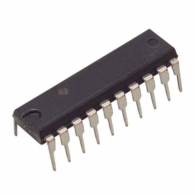
DW OR N PACKAGE
(TOP VIEW)
BiCMOS Design Significantly Reduces ICCZ
3-State True Outputs Drive Bus Lines
Directly
High-Impedance State During Power Up
and Power Down
ESD Protection Exceeds 2000 V
Per MIL-STD-883C, Method 3015
Package Options Include Plastic
Small-Outline (DW) Packages and Standard
Plastic 300-mil DIPs (N)
DIR
A1
A2
A3
A4
A5
A6
A7
A8
GND
description
1
20
2
19
3
18
4
17
5
16
6
15
7
14
8
13
9
12
10
11
VCC
OE
B1
B2
B3
B4
B5
B6
B7
B8
This octal bus transceiver is designed for
asynchronous communication between data
buses. The devices transmit data from the A bus to the B bus or from the B bus to the A bus depending upon
the logic level at the direction-control (DIR) input. The output-enable (OE) input can be used to disable the device
so the buses are effectively isolated.
The outputs are in a high-impedance state during power up and power down while the supply voltage is less
than approximately 3 V.
The SN64BCT245 is characterized for operation from − 40°C to 85°C and 0°C to 70°C.
FUNCTION TABLE
INPUTS
OE
L
L
B data to A bus
L
H
A data to B bus
H
X
Isolation
logic symbol†
OE
DIR
A1
19
1
2
OPERATION
DIR
logic diagram (positive logic)
DIR
G3
1
3EN1[BA]
3EN2[AB]
19
18
1
B1
A1
OE
2
2
A2
A3
A4
A5
A6
A7
A8
3
17
4
16
5
15
6
14
7
13
8
12
9
11
B2
18
B3
B1
B4
B5
B6
B7
To Seven Other Channels
B8
† This symbol is in accordance with ANSI/IEEE Std 91-1984
and IEC Publication 617-12.
Copyright 1994, Texas Instruments Incorporated
��
�����
� ���� �������!��� �" #$��%�! �" �� &$'(�#�!��� )�!%*
���)$#!" #������ !� "&%#���#�!���" &%� !+% !%��" �� �%,�" ��"!�$�%�!"
"!��)��) -�����!.* ���)$#!��� &��#%""��/ )�%" ��! �%#%""���(. ��#($)%
!%"!��/ �� �(( &����%!%�"*
• DALLAS, TEXAS 75265
• HOUSTON, TEXAS 77251−1443
POST OFFICE BOX 655303
POST OFFICE BOX 1443
3−1
����������
����
���
�����������
����
�������
������
SCBS040A − JANUARY 1990 − REVISED JANUARY 1994
absolute maximum ratings over operating free-air temperature range (unless otherwise noted)†
Supply voltage range, VCC . . . . . . . . . . . . . . . . . . . . . . . . . . . . . . . . . . . . . . . . . . . . . . . . . . . . . . . . . . − 0.5 V to 7 V
Input voltage range, VI (see Note 1) . . . . . . . . . . . . . . . . . . . . . . . . . . . . . . . . . . . . . . . . . . . . . . . . . . . − 0.5 V to 7 V
Voltage range applied to any output in the disabled or power-off state, VO . . . . . . . . . . . . . . . − 0.5 V to 5.5 V
Voltage range applied to any output in the high state, VO . . . . . . . . . . . . . . . . . . . . . . . . . . . . . . . − 0.5 V to VCC
Current into any output in the low state . . . . . . . . . . . . . . . . . . . . . . . . . . . . . . . . . . . . . . . . . . . . . . . . . . . . . 128 mA
Operating free-air temperature range . . . . . . . . . . . . . . . . . . . . . . . . . . . . . . . . . . . . . . . . . . . . . . . . − 40°C to 85°C
Storage temperature range . . . . . . . . . . . . . . . . . . . . . . . . . . . . . . . . . . . . . . . . . . . . . . . . . . . . . . . . − 65°C to 150°C
† Stresses beyond those listed under “absolute maximum ratings” may cause permanent damage to the device. These are stress ratings only, and
functional operation of the device at these or any other conditions beyond those indicated under “recommended operating conditions” is not
implied. Exposure to absolute-maximum-rated conditions for extended periods may affect device reliability.
NOTE 1: The input and output voltage ratings may be exceeded if the input and output current ratings are observed.
recommended operating conditions
MIN
NOM
MAX
4.5
5
5.5
UNIT
VCC
VIH
Supply voltage
VIL
IIK
Low-level input voltage
0.8
V
Input clamp current
−18
mA
IOH
High-level output current
IOL
Low-level output current
TA
Operating free-air temperature
3−2
High-level input voltage
2
A1 −A8
−3
−15
A1 −A8
24
B1 −B8
64
•
POST OFFICE BOX 655303 DALLAS, TEXAS 75265
POST OFFICE BOX 1443 HOUSTON, TEXAS 77251−1443
•
V
B1 −B8
−40
V
85
mA
mA
°C
����������
����
���
�����������
����
�������
������
SCBS040A − JANUARY 1990 − REVISED JANUARY 1994
electrical characteristics over recommended operating free-air temperature range (unless
otherwise noted)
PARAMETER
VIK
TEST CONDITIONS
VCC = 4.5 V,
II = −18 mA
IOH = −1 mA
VCC = 4.5 V
IOH = − 3 mA
IOH = −15 mA
Any A
Any A or B
VOH
Any B
Any A
VOL
MIN
Any B
VCC = 4.5 V
IOL = 24 mA
IOL = 64 mA
Power up
VCC = 0 to 2.3 V
VO = 2.7 V
VO = 0.5 V
OE at 0.8 V
Power down
VCC = 1.8 V to 0
VO = 2.7 V
VO = 0.5 V
OE at 0.8 V
IOZ
TYP†
2.5
3.4
2.4
3.3
2
3.1
UNIT
−1.2
V
V
0.35
0.5
0.42
0.55
DIR and OE
70
µA
mA
70
µA
−0.65
mA
1
VCC = 5.5 V,
VI = 5.5 V
VCC = 5.5 V,
VI = 2.7 V
VCC = 5.5 V,
VI = 0.5 V
VCC = 5.5 V,
VO = 0
0.1
A and B
IIH‡
DIR and OE
70
20
A and B
IIL
DIR and OE
Any B
ICCH
ICCL
ICCZ
Ci
A-to-B
A-to-B
VCC = 5.5 V
VCC = 5.5 V
OE and DIR
VCC = 5.5 V
VCC = 5 V,
A to B
B to A
mA
µA
A
−0.65
−1.2
Any A
IOS§
V
−0.65
A and B
II‡
Cio
MAX
−60
−150
−100
−225
VI = 2.5 V or 0.5 V
VCC = 5 V,
36
57
57
90
10
15
7
mA
mA
pF
9
VI = 2.5 V or 0.5 V
mA
pF
12
† All typical values are at VCC = 5 V, TA = 25°C.
‡ For I/O ports, the parameters IIH and IIL include the off-state output current.
§ Not more than one output should be tested at a time, and the duration of the test should not exceed one second.
switching characteristics (see Note 2)
PARAMETER
FROM
(INPUT)
TO
(OUTPUT)
tPLH
tPHL
A or B
B or A
tPZH
tPZL
OE
A or B
tPHZ
tPLZ
OE
A or B
VCC = 5 V,
CL = 50 pF,
R1 = 500 Ω,
R2 = 500 Ω,
TA = 25°C
VCC = 4.5 V to 5.5 V,
CL = 50 pF,
R1 = 500 Ω,
R2 = 500 Ω
UNIT
TA = − 40°C
to 85°C
TA = 0°C
to 70°C
MIN
MAX
MIN
MAX
MIN
MAX
1
6
1
7.2
1
7
1.5
6.6
1.5
7.6
1.5
7
1.5
9.4
1.5
11.2
1.5
10.9
1.5
10.2
1.5
11.8
1.5
11.6
1.5
8.3
1.5
9.7
1.5
9.3
1.5
7.8
1.5
9.6
1.5
9.1
ns
ns
ns
NOTE 2: Load circuits and voltage waveforms are shown in Section 1.
•
POST OFFICE BOX 655303 DALLAS, TEXAS 75265
POST OFFICE BOX 1443 HOUSTON, TEXAS 77251−1443
•
3−3
����������
����
���
�����������
����
�������
������
SCBS040A − JANUARY 1990 − REVISED JANUARY 1994
3−4
•
POST OFFICE BOX 655303 DALLAS, TEXAS 75265
POST OFFICE BOX 1443 HOUSTON, TEXAS 77251−1443
•
�PACKAGE OPTION ADDENDUM
www.ti.com
14-Oct-2022
PACKAGING INFORMATION
Orderable Device
Status
(1)
Package Type Package Pins Package
Drawing
Qty
Eco Plan
(2)
Lead finish/
Ball material
MSL Peak Temp
Op Temp (°C)
Device Marking
(3)
Samples
(4/5)
(6)
SN64BCT245DW
ACTIVE
SOIC
DW
20
25
RoHS & Green
NIPDAU
Level-1-260C-UNLIM
-40 to 85
6BCT245
(1)
The marketing status values are defined as follows:
ACTIVE: Product device recommended for new designs.
LIFEBUY: TI has announced that the device will be discontinued, and a lifetime-buy period is in effect.
NRND: Not recommended for new designs. Device is in production to support existing customers, but TI does not recommend using this part in a new design.
PREVIEW: Device has been announced but is not in production. Samples may or may not be available.
OBSOLETE: TI has discontinued the production of the device.
(2)
RoHS: TI defines "RoHS" to mean semiconductor products that are compliant with the current EU RoHS requirements for all 10 RoHS substances, including the requirement that RoHS substance
do not exceed 0.1% by weight in homogeneous materials. Where designed to be soldered at high temperatures, "RoHS" products are suitable for use in specified lead-free processes. TI may
reference these types of products as "Pb-Free".
RoHS Exempt: TI defines "RoHS Exempt" to mean products that contain lead but are compliant with EU RoHS pursuant to a specific EU RoHS exemption.
Green: TI defines "Green" to mean the content of Chlorine (Cl) and Bromine (Br) based flame retardants meet JS709B low halogen requirements of
很抱歉,暂时无法提供与“SN64BCT245N”相匹配的价格&库存,您可以联系我们找货
免费人工找货