Product
Folder
Order
Now
Support &
Community
Tools &
Software
Technical
Documents
SN65DSI85-Q1
SLLSEJ4B – JULY 2016 – REVISED JUNE 2018
SN65DSI85-Q1 Automotive Dual-Channel MIPI® DSI to Dual-Link LVDS Bridge
1 Features
2 Applications
•
•
•
•
•
•
•
•
•
•
•
•
•
•
•
•
•
•
•
•
•
•
•
Qualified for Automotive Applications
AEC-Q100 Qualified With the Following Results:
– Device Temperature Grade 2: –40°C to 105°C
Ambient Operating Temperature
– Device HBM ESD Classification Level 3A
– Device CDM ESD Classification Level C6
Implements MIPI D-PHY Version 1.00.00 Physical
Layer Front-End and Display Serial Interface (DSI)
Version 1.02.00
Dual-Channel DSI Receiver Configurable for One,
Two, Three, or Four D-PHY Data Lanes Per
Channel Operating up to 1 Gbps Per Lane
Supports 18-bpp and 24-bpp DSI Video Packets
with RGB666 and RGB888 Formats
Suitable for 60-fps WQXGA 2560 × 1600
Resolution at 18-bpp and 24-bpp Color, and 60
fps (120 fps Equivalent) WUXGA 1920 × 1200
Resolution With 3D Graphics at 24-bpp Color
MIPI Front-End Configurable for Single-Channel
or Dual-Channel DSI Configurations
Output Configurable for Single-Link or Dual-Link
LVDS
Supports Dual-Channel DSI ODD or EVEN and
LEFT or RIGHT Operating Modes
Supports Two Single-Channel DSI to Two SingleLink LVDS Operating Mode
LVDS Output-Clock Range of 25 MHz to 154 MHz
in Dual-Link or Single-Link Mode
LVDS Pixel Clock May be Sourced from FreeRunning Continuous D-PHY Clock or External
Reference Clock (REFCLK)
1.8-V Main VCC Power Supply
Low Power Features Include SHUTDOWN Mode,
Reduced LVDS Output Voltage Swing, Common
Mode, and MIPI Ultra-Low Power State (ULPS)
Support
LVDS Channel SWAP, LVDS PIN Order Reverse
Feature for Ease of PCB Routing
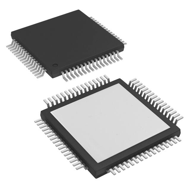
Packaged in 64-pin 10 mm × 10 mm HTQFP
(PAP) PowerPAD™ IC Package
Infotainment Head Unit With Integrated Display
Infotainment Head Unit With Remote Display
Infotainment Rear-Seat Entertainment
Hybrid Automotive Cluster
Portable Navigation Device
Navigation
Industrial Human Machine Interface (HMI) and
Displays
3 Description
The SN65DSI85-Q1 DSI-to-LVDS bridge features a
dual-channel MIPI D-PHY receiver front-end
configuration with four lanes per channel operating at
1 Gbps per lane and a maximum input bandwidth of 8
Gbps. The bridge decodes MIPI DSI 18-bpp RGB666
and 24-bpp RGB888 packets and converts the
formatted video data-stream to an LVDS output
operating at pixel clocks operating from 25 MHz to
154 MHz, offering a dual-link LVDS, single-link LVDS,
or two Single-Link LVDS interfaces with four data
lanes per link.
The SN65DSI85-Q1 device is well suited for WQXGA
(2560 × 1600) at 60 frames per second (fps), as well
as 3D Graphics at WUXGA and True HD (1920 ×
1080) resolutions at an equivalent 120 fps with up to
24 bits-per-pixel (bpp). Partial line buffering is
implemented to accommodate the data stream
mismatch between the DSI and LVDS interfaces.
The SN65DSI85-Q1 device is implemented in a small
outline 10 mm × 10 mm HTQFP package with a
0.5-mm pitch, and operates across a temperature
range from –40°C to 105°C.
Device Information(1)
PART NUMBER
SN65DSI85-Q1
PACKAGE
HTQFP (64)
BODY SIZE (NOM)
10.00 mm × 10.00 mm
(1) For all available packages, see the orderable addendum at
the end of the data sheet.
Typical Application
DA[3:0]P
DA[3:0]N
Application
Processor
With DSI
Output
DACP/N
DB[3:0]P
TFT LCD Display
A_Y0:3N
Dual-Channel
DSI to LVDS
Bridge
SN65SDSI85-Q1
A_Y0:3P
A_CLKN/P
B_Y0:3N
DB[3:0]N
B_Y0:3P
SCL/SDA
B_CLKN/P
24-Bit TCON
1
Copyright © 2016, Texas Instruments Incorporated
1
An IMPORTANT NOTICE at the end of this data sheet addresses availability, warranty, changes, use in safety-critical applications,
intellectual property matters and other important disclaimers. PRODUCTION DATA.
�SN65DSI85-Q1
SLLSEJ4B – JULY 2016 – REVISED JUNE 2018
www.ti.com
Table of Contents
1
2
3
4
5
6
7
8
Features ..................................................................
Applications ...........................................................
Description .............................................................
Revision History.....................................................
Pin Configuration and Functions .........................
Specifications.........................................................
1
1
1
2
3
5
6.1
6.2
6.3
6.4
6.5
6.6
5
5
6
6
6
9
Absolute Maximum Ratings ......................................
ESD Ratings..............................................................
Recommended Operating Conditions.......................
Thermal Information ..................................................
Electrical Characteristics...........................................
Switching Characteristics ..........................................
Parameter Measurement Information ................ 10
Detailed Description ............................................ 13
8.1
8.2
8.3
8.4
8.5
Overview .................................................................
Functional Block Diagram .......................................
Feature Description.................................................
Device Functional Modes........................................
Programming...........................................................
13
13
14
24
24
8.6 Register Maps ......................................................... 25
9
Application and Implementation ........................ 53
9.1 Application Information............................................ 53
9.2 Typical Applications ................................................ 54
10 Power Supply Recommendations ..................... 60
10.1 VCC Power Supply................................................. 60
10.2 VCORE Power Supply .......................................... 60
11 Layout................................................................... 60
11.1 Layout Guidelines ................................................. 60
11.2 Layout Example .................................................... 61
12 Device and Documentation Support ................. 62
12.1
12.2
12.3
12.4
12.5
12.6
Documentation Support ........................................
Receiving Notification of Documentation Updates
Community Resource............................................
Trademarks ...........................................................
Electrostatic Discharge Caution ............................
Glossary ................................................................
62
62
62
62
62
62
13 Mechanical, Packaging, and Orderable
Information ........................................................... 62
4 Revision History
NOTE: Page numbers for previous revisions may differ from page numbers in the current version.
Changes from Revision A (December 2016) to Revision B
Page
•
Deleted figure RESET and Initialization Timing Definition While VCC is High ...................................................................... 12
•
Changed the paragraph following Figure 8 ......................................................................................................................... 14
•
Changed Table 1 .................................................................................................................................................................. 15
Changes from Original (July 2016) to Revision A
•
2
Page
Changed device to Production Data....................................................................................................................................... 1
Submit Documentation Feedback
Copyright © 2016–2018, Texas Instruments Incorporated
Product Folder Links: SN65DSI85-Q1
�SN65DSI85-Q1
www.ti.com
SLLSEJ4B – JULY 2016 – REVISED JUNE 2018
5 Pin Configuration and Functions
V
A_Y1P
V
A_Y2N
A_Y2P
V
A_CLKN
A_CLKP
A_Y3N
A_Y3P
V
RSVD1
IRQ
44
43
42
41
40
39
38
37
36
35
34
33
CC
CC
CC
A_Y1N
45
A_Y0P
46
A_Y0N
47
CC
V
48
PAP Package
64-Pin HTQFP With PowerPAD™
Top View
49
32
V
B_Y3P
50
31
VCORE
B_Y3N
51
30
DA3N
GND
52
29
DA3P
B_CLKP
53
28
DA2N
B_CLKN
54
27
DA2P
55
26
GND
25
DACN
57
24
DACP
58
23
GND
B_Y1P
59
22
DA1N
B_Y1N
60
21
DA1P
B_Y0P
61
20
DA0N
B_Y0N
62
19
DA0P
63
18
V
64
17
REFCLK
V
CC
CC
B_Y2P
56
CC
Thermal
8
9
10
11
12
13
14
DBCP
DBCN
DB2P
DB2N
DB3P
DB3N
V
CC
CC
16
7
DB1N
SDA
6
DB1P
15
5
DB0N
SCL
4
DB0P
3
V
CC
ADDR
2
CC
EN
V
CC
1
V
RSVD2
Pad
B_Y2N
See the Layout section for layout information.
Submit Documentation Feedback
Copyright © 2016–2018, Texas Instruments Incorporated
Product Folder Links: SN65DSI85-Q1
3
�SN65DSI85-Q1
SLLSEJ4B – JULY 2016 – REVISED JUNE 2018
www.ti.com
Pin Functions
PIN
TYPE
DESCRIPTION
64
I/O
Local I2C interface target address select. See Table 6. In normal operation this pin is an
input. When the ADDR pin is programmed high, it must be tied to the same 1.8-V power
rails where the SN65DSI85-Q1 VCC 1.8-V power rail is connected.
A_Y0P
46
O
A_Y0N
47
O
A_Y1P
44
O
A_Y1N
45
O
A_Y2P
41
O
A_Y2N
42
O
A_Y3P
36
O
A_Y3N
37
O
A_CLKP
38
O
A_CLKN
39
O
B_Y0P
61
O
B_Y0N
62
O
B_Y1P
59
O
B_Y1N
60
O
B_Y2P
56
O
B_Y2N
57
O
B_Y3P
50
O
B_Y3N
51
O
B_CLKP
53
O
B_CLKN
54
O
DA0P
19
I
DA0N
20
I
DA1P
21
I
DA1N
22
I
DA2P
27
I
DA2N
28
I
DA3P
29
I
DA3N
30
I
DACP
24
I
DACN
25
I
DB0P
4
I
DB0N
5
I
DB1P
6
I
DB1N
7
I
DB2P
10
I
DB2N
11
I
DB3P
12
I
DB3N
13
I
DBCP
8
I
DBCN
9
I
NAME
NO.
ADDR
EN
GND
4
2
I
23
G
26
G
52
G
LVDS channel A, LVDS data output 0
LVDS channel A, LVDS data output 1
LVDS channel A, LVDS data output 2
LVDS channel A, LVDS data output 3. A_Y3P and A_Y3N must be left not connected
(NC) for 18-bpp panels.
LVDS channel A, LVDS clock output
LVDS channel B, LVDS data output 0
LVDS channel B, LVDS data output 1
LVDS channel B, LVDS data output 2
LVDS channel B, LVDS data output 3. B_Y3P and B_Y3N must be left NC for 18-bpp
panels.
LVDS channel B, LVDS clock output
MIPI D-PHY channel A, data lane 0; data rate up to 1 Gbps.
MIPI D-PHY channel A, data lane 1; data rate up to 1 Gbps
MIPI D-PHY channel A, data lane 2; data rate up to 1 Gbps.
MIPI D-PHY channel A, data lane 3; data rate up to 1 Gbps.
MIPI D-PHY channel A, clock lane; data rate up to 1 Gbps.
MIPI D-PHY channel B, data lane 0; data rate up to 1 Gbps.
MIPI D-PHY channel B, data lane 1; data rate up to 1 Gbps.
MIPI D-PHY channel B, data lane 2; data rate up to 1 Gbps.
MIPI D-PHY channel B, data lane 3; data rate up to 1 Gbps.
MIPI D-PHY channel B, clock lane; operates up to 1 Gbps.
Chip enable and reset. The device is reset (shutdown) when the EN pin is low.
Reference ground
Submit Documentation Feedback
Copyright © 2016–2018, Texas Instruments Incorporated
Product Folder Links: SN65DSI85-Q1
�SN65DSI85-Q1
www.ti.com
SLLSEJ4B – JULY 2016 – REVISED JUNE 2018
Pin Functions (continued)
PIN
NAME
NO.
TYPE
DESCRIPTION
IRQ
33
O
Interrupt signal
REFCLK
17
I
This pin is an optional external reference clock for the LVDS pixel clock. If an external
reference clock is not used, this pin must be pulled to ground with an external resistor.
The source of the reference clock must be placed as close as possible with a series
resistor near the source to reduce EMI.
RSVD1
34
I/O
Reserved. This pin must be left unconnected for normal operation.
RSVD2
1
I
Reserved. This pin must be left unconnected for normal operation.
SCL
15
I
Local I2C interface clock.
SDA
16
I/O
3
—
14
—
18
—
32
—
35
—
40
—
43
—
48
—
49
—
55
—
58
—
63
—
31
P
1.1-V output from the voltage regulator. This pin must have a 1-µF external capacitor to
ground.
—
Reference ground
VCC
VCORE
PowerPAD
Local I2C interface data
1.8-V power supply
6 Specifications
6.1 Absolute Maximum Ratings
over operating free-air temperature range (unless otherwise noted) (1)
VCC
MIN
MAX
UNIT
–0.3
2.175
V
CMOS input pins
–0.5
2.175
V
DSI input pins (DAxP, DAxN, DBxP, and DBxN)
–0.4
1.4
V
Supply voltage
Input voltage
TA
Operating free-air temperature
–40
105
°C
TJ
Junction temperature
–40
115
°C
Tstg
Storage temperature
–65
150
°C
(1)
Stresses beyond those listed under Absolute Maximum Ratings may cause permanent damage to the device. These are stress ratings
only, which do not imply functional operation of the device at these or any other conditions beyond those indicated under Recommended
Operating Conditions. Exposure to absolute-maximum-rated conditions for extended periods may affect device reliability.
6.2 ESD Ratings
VALUE
V(ESD)
(1)
Electrostatic
discharge
Human-body model (HBM), per AEC Q100-002
(1)
Charged-device model (CDM), per AEC Q100-011
UNIT
±4000
±1000
V
AEC Q100-002 indicates that HBM stressing shall be in accordance with the ANSI/ESDA/JEDEC JS-001 specification.
Submit Documentation Feedback
Copyright © 2016–2018, Texas Instruments Incorporated
Product Folder Links: SN65DSI85-Q1
5
�SN65DSI85-Q1
SLLSEJ4B – JULY 2016 – REVISED JUNE 2018
www.ti.com
6.3 Recommended Operating Conditions
over operating free-air temperature range (unless otherwise noted)
MIN
NOM
MAX
UNIT
1.65
1.8
1.95
V
VCC
VCC power supply
VPSN
Supply noise on any VCC pin
V(DSI)
DSI input pin voltage
ƒ(I2C)
Local I2C input frequency
ƒHS(CLK)
DSI high-speed (HS) clock input frequency
tsu
DSI HS data to clock setup time; see Figure 1
0.15
UI (1)
th
DSI HS data to clock hold time; see Figure 1
0.15
UI (1)
ZOD(LVDS)
LVDS output differential impedance
TC
Case temperature
(1)
ƒ(noise) > 1 MHz
0.05
V
–50
1350
mV
400
kHz
500
MHz
40
90
132
Ω
92.2
°C
The unit interval (UI) is one half of the period of the HS clock; at 500 MHz the minimum setup and hold time is 150 ps.
6.4 Thermal Information
SN65DSI85-Q1
THERMAL METRIC (1)
PAP (HTQFP)
UNIT
64 PINS
RθJA
Junction-to-ambient thermal resistance
36.1
°C/W
RθJC(top)
Junction-to-case (top) thermal resistance
18.2
°C/W
RθJB
Junction-to-board thermal resistance
20.6
°C/W
ψJT
Junction-to-top characterization parameter
0.8
°C/W
ψJB
Junction-to-board characterization parameter
20.5
°C/W
RθJC(bot)
Junction-to-case (bottom) thermal resistance
2.2
°C/W
(1)
For more information about traditional and new thermal metrics, see the Semiconductor and IC Package Thermal Metrics application
report.
6.5 Electrical Characteristics
over operating free-air temperature range (unless otherwise noted)
PARAMETER
TEST CONDITIONS
MIN
TYP (1)
MAX
Low-level control signal input voltage
VIH
High-level control signal input voltage
VOH
High-level output voltage
IOH = –4 mA
VOL
Low-level output voltage
IOL = 4 mA
0.4
V
ILKG
Input failsafe leakage current
VCC = 0; VCC(PIN) = 1.8 V
±30
μA
IIH
High level input current
Any input terminal
±30
μA
IIL
Low level input current
Any input terminal
±30
μA
IOZ
High-impedance output current
CMOS output terminals
±10
μA
IOS
Short-circuit output current
Any output driving GND short
±50
mA
ICC
Device active current
See
127
232
mA
IULPS
Device standby current
All data and clock lanes are in ultra-low
power state (ULPS)
7.7
14
mA
IRST
Shutdown current
EN = 0
0.04
130
µA
REN
EN control input resistor
(1)
(2)
6
0.3 × VCC
UNIT
VIL
(2)
V
0.7 × VCC
V
1.25
V
200
kΩ
All typical values are at VCC = 1.8V and TA = 25°C
SN65DSI85-Q1: DUAL Channel DSI to DUAL Channel LVDS, 1920 x 1200
(a) number of LVDS lanes = 2 × (3 data lanes + 1 CLK lane)
(b) number of DSI lanes = 2 × (4 data lanes + 1 CLK lane
(c) LVDS CLK OUT = 81.6 M
(d) DSI CLK = 490 M
(e) RGB888, LVDS18bpp
Maximum values are at VCC = 1.95 V and TA = 105°C
Submit Documentation Feedback
Copyright © 2016–2018, Texas Instruments Incorporated
Product Folder Links: SN65DSI85-Q1
�SN65DSI85-Q1
www.ti.com
SLLSEJ4B – JULY 2016 – REVISED JUNE 2018
Electrical Characteristics (continued)
over operating free-air temperature range (unless otherwise noted)
PARAMETER
TEST CONDITIONS
MIN
TYP (1)
MAX
UNIT
MIPI DSI INTERFACE
VIH-LP
LP receiver input high threshold
See Figure 2
VIL-LP
LP receiver input low threshold
See Figure 2
|VID|
HS differential input voltage
|VIDT|
HS differential input voltage threshold
VIL-ULPS
LP receiver input low threshold; ultra-low
power state (ULPS)
VCM-HS
HS common mode voltage; steady-state
ΔVCM-HS
HS common mode peak-to-peak variation
including symbol delta and interference
VIH-HS
HS single-ended input high voltage
See Figure 2
VIL-HS
HS single-ended input low voltage
See Figure 2
VTERM-EN
HS termination enable; single-ended input
Termination is switched simultaneous for
voltage (both Dp AND Dn apply to
Dn and Dp
enable)
RDIFF-HS
HS mode differential input impedance
880
mV
100
70
550
mV
270
mV
50
mV
300
mV
330
mV
100
mV
460
mV
–40
mV
80
450
mV
125
Ω
LVDS OUTPUT
|VOD|
Steady-state differential output voltage for
A_Yx P/N and B_Yx P/N
CSR 0x19.3:2=00 and, or CSR
0x19.1:0=00
100 Ω near end termination
180
245
330
CSR 0x19.3:2=01 and, or CSR
0x19.1:0=01
100 Ω near end termination
215
293
392
CSR 0x19.3:2=10 and, or CSR
0x19.1:0=10
100 Ω near end termination
250
341
455
CSR 0x19.3:2=11 and, or CSR
0x19.1:0=11
100 Ω near end termination
290
389
515
CSR 0x19.3:2=00 and, or CSR
0x19.1:0=00
200 Ω near end termination
150
204
275
CSR 0x19.3:2=01 and, or CSR
0x19.1:0=01
200 Ω near end termination
200
271
365
CSR 0x19.3:2=10 and, or CSR
0x19.1:0=10
200 Ω near end termination
250
337
450
CSR 0x19.3:2=11 and, or CSR
0x19.1:0=11
200 Ω near end termination
300
402
535
mV
Submit Documentation Feedback
Copyright © 2016–2018, Texas Instruments Incorporated
Product Folder Links: SN65DSI85-Q1
7
�SN65DSI85-Q1
SLLSEJ4B – JULY 2016 – REVISED JUNE 2018
www.ti.com
Electrical Characteristics (continued)
over operating free-air temperature range (unless otherwise noted)
PARAMETER
Steady-state differential output voltage for
A_CLKP/N and B_CLKP/N
|VOD|
Δ|VOD|
Change in steady-state differential output
voltage between opposite binary states
VOC(SS)
Steady state common-mode output
voltage (3)
VOC(PP)
Peak-to-peak common-mode output
voltage
RLVDS_DIS
Pulldown resistance for disabled LVDS
outputs
(3)
8
TEST CONDITIONS
MIN
TYP (1)
MAX
CSR 0x19.3:2=00 and, or CSR
0x19.1:0=00
100 Ω near end termination
140
191
262
CSR 0x19.3:2=01 and, or CSR
0x19.1:0=01
100 Ω near end termination
168
229
315
CSR 0x19.3:2=10 and, or CSR
0x19.1:0=10
100 Ω near end termination
195
266
365
CSR 0x19.3:2=11 and, or CSR
0x19.1:0=11
100 Ω near end termination
226
303
415
CSR 0x19.3:2=00 and, or CSR
0x19.1:0=00
200 Ω near end termination
117
159
220
CSR 0x19.3:2=01 and, or CSR
0x19.1:0=01
200 Ω near end termination
156
211
295
CSR 0x19.3:2=10 and, or CSR
0x19.1:0=10
200 Ω near end termination
195
263
362
CSR 0x19.3:2=11 and, or CSR
0x19.1:0=11
200 Ω near end termination
234
314
435
mV
RL = 100 Ω
CSR 0x19.6 = 1 and CSR 0x1B.6 = 1;
and, or CSR 0x19.4 = 1 and
CSR 0x1B.4 = 1; see Figure 3
CSR 0x19.6 = 0 and, or CSR 0x19.4 = 0;
see Figure 3
UNIT
35
0.75
0.9
mV
1.13
V
1
1.25
see Figure 3
1.5
35
1
mV
kΩ
Tested at VCC = 1.8V , TA = –40°C for MIN, TA = 25°C for TYP, TA = 105°C for MAX.
Submit Documentation Feedback
Copyright © 2016–2018, Texas Instruments Incorporated
Product Folder Links: SN65DSI85-Q1
�SN65DSI85-Q1
www.ti.com
SLLSEJ4B – JULY 2016 – REVISED JUNE 2018
6.6 Switching Characteristics
over operating free-air temperature range (unless otherwise noted)
PARAMETER
TEST CONDITIONS
MIN
TYP (1)
MAX
UNIT
300
ps
40
ns
DSI
tGS
DSI LP glitch suppression pulse width
LVDS
tc
Output clock period
tw
High-level output clock (CLK) pulse duration
6.49
t0
Delay time, CLK↑ to 1st serial bit position
t1
Delay time, CLK↑ to 2nd serial bit position
t2
Delay time, CLK↑ to 3rd serial bit position
t3
Delay time, CLK↑ to 4th serial bit position
t4
Delay time, CLK↑ to 5th serial bit position
t5
t6
tr
Differential output rise-time
tf
Differential output fall-time
4/7 tc
ns
–0.15
0.15
ns
1/7 tc – 0.15
1/7 tc + 0.15
ns
2/7 tc – 0.15
2/7 tc + 0.15
ns
3/7 tc – 0.15
3/7 tc + 0.15
ns
4/7 tc – 0.15
4/7 tc + 0.15
ns
Delay time, CLK↑ to 6th serial bit position
5/7 tc – 0.15
5/7 tc + 0.15
ns
Delay time, CLK↑ to 7th serial bit position
6/7 tc – 0.15
6/7 tc + 0.15
ns
180
500
ps
–10
10
ps
tc = 6.49 ns;
Input clock jitter < 25 ps
(REFCLK)
See Figure 4
See Figure 4
LVDS CLK A to CLK B skew
EN, ULPS, RESET
ten
Enable time from EN or ULPS; see
tc(o) = 12.9 ns
1
ms
tdis
Disable time to standby
tc(o) = 12.9 ns
0.1
ms
treset
Reset Time
10
FREFCLK
REFCLK Freqeuncy. Supported frequencies:
25 MHz - 15 4MHz
25
154
tr, tf
REFCLK rise and fall time
100ps
1ns
s
tpj
REFCLK Peak-to-Peak Phase Jitter
50
ps
Duty
REFCLK Duty Cycle
ms
REFCLK
40%
50%
60%
0.5%
1%
2%
MHz
REFCLK or DSI CLK (DACP/N, DBCP/N)
SSC_CLKIN
(1)
(2)
SSC enabled Input CLK center spread depth (2)
Modulation Frequency Range
30
60
kHz
All typical values are at VCC = 1.8 V and TA = 25°C
For EMI reduction purpose, SN65DSI85-Q1 supports the center spreading of the LVDS CLK output through the REFCLK or DSI CLK
input. The center spread CLK input to the REFCLK or DSI CLK is passed through to the LVDS CLK output A_CLKP/N and/or
B_CLKP/N.
Submit Documentation Feedback
Copyright © 2016–2018, Texas Instruments Incorporated
Product Folder Links: SN65DSI85-Q1
9
�SN65DSI85-Q1
SLLSEJ4B – JULY 2016 – REVISED JUNE 2018
www.ti.com
7 Parameter Measurement Information
th
DACP, DACN
DBCP, DBCN
...
tsu
...
DAxP, DAxN
DBxP, DBxN
1 UI
Figure 1. DSI HS Mode Receiver Timing Definitions
1.3 V
LP-RX
Input HIGH
VIH(LP)
VIL(LP)
VID
LP-RX
Input LOW
VIH(HS)
VCM(HS)max
HS-RX
Common Mode
Range
VCM(HS)min
GND
VIL(HS)
Low Power (LP)
Mode Receiver
High Speed (HS) Mode
Receiver
Figure 2. DSI Receiver Voltage Definitions
10
Submit Documentation Feedback
Copyright © 2016–2018, Texas Instruments Incorporated
Product Folder Links: SN65DSI85-Q1
�SN65DSI85-Q1
www.ti.com
SLLSEJ4B – JULY 2016 – REVISED JUNE 2018
Parameter Measurement Information (continued)
A_YnP
B_YnP
49.9 Ω ±1% (2 PLCS)
VOD
A_YnN
B_YnN
VOC
100 %
80%
VOD(H)
0V
VOD(L)
20%
0%
tf
tr
VOC(PP)
VOC(s)
VOC(s)
0V
Figure 3. Test Load and Voltage Definitions for LVDS Outputs
CLK
td(6)
td(5)
td(4)
td(3)
td(2)
td(1)
td(0)
Yn
VOD(H)
0V
VOD(L)
td(0) to td(6)
Figure 4. SN65DSI85-Q1 LVDS Timing Definitions
Submit Documentation Feedback
Copyright © 2016–2018, Texas Instruments Incorporated
Product Folder Links: SN65DSI85-Q1
11
�SN65DSI85-Q1
SLLSEJ4B – JULY 2016 – REVISED JUNE 2018
www.ti.com
Parameter Measurement Information (continued)
ULPS (LP00) State
DSI lane
ten
tdis
A_CLKP/N
(LVDS_CHA_CLK)
(1)
See the ULPS section of the data sheet for the ULPS entry and exit sequence.
(2)
ULPS entry and exit protocol and timing requirements must be met according to the MIPI DPHY specification.
Figure 5. ULPS Timing Definition
12
Submit Documentation Feedback
Copyright © 2016–2018, Texas Instruments Incorporated
Product Folder Links: SN65DSI85-Q1
�SN65DSI85-Q1
www.ti.com
SLLSEJ4B – JULY 2016 – REVISED JUNE 2018
8 Detailed Description
8.1 Overview
The SN65DSI85-Q1 device is an AEC-Q100 qualified, 2-channel MIPI DSI to dual-link LVDS transmitter. The
device features a dual-channel MIPI D-PHY receiver front-end configurable for 1 to 4 data lanes per channel
operating at 1 Gbps/lane for a maximum input bandwidth of 8 Gbps. This device decodes MIPI DSI 18-bpp
RGB666 and 24-bpp RGB888 data stream and converts it to an LVDS output operating at pixel-clock frequencies
of 25 MHz to 154 MHz. The LVDS output can be configured as a dual-link LVDS, two single-link LVDS, or a
single-link LVDS output interface with four data lanes per link.
8.2 Functional Block Diagram
AVCC
DSI Packet
Processors
AGND
VCC
ULPS
GND
Lane ERR
Merge
LPRX
A_YNP
A_Y1N
(Odd)
18
HSRX
DA0N
Long
Packets
Data Lane 0
7-Bit Shift
Register
DA1N
DA2P
DA2N
DA3P
DA3N
Data Lane 1
(Circuit same as Data Lane 0)
8
Data Lane 2
(Circuit same as Data Lane 0)
8
Data Lane 3
(Circuit same as Data Lane 0)
8
A_Y3P
Timers
Short
Packets
A_Y3N
SOT
ULPS
32
DSI Channel
Merging
Channel
Formatter
LVDSPLL
PLL
Lock
HSRX
Pixel Clock
DB0P
DB0N
8
DB1P
8
DB1N
Channel B
8
(Circuit same as Channel A)
DB3P
Lane
Merge
CSR
HS-Clock
Sourced
M/N Pixel Clock
PLL
B_Y2P
B_CLKP
B_CLKN
B_Y3P
Clock Circuits
CLK Lane
B_Y1N
B_Y2N
LPRX
DB2N
B_Y0N
Partial
Line Buffer
DACP
DB2P
B_Y0P
DE
VS
HS
B_Y1P
EOT
DACN
A_Y2N
A_CLKN
SOT
32
A_Y2P
A_CLKP
(Even)
18
EOT
DA1P
A_Y0P
A_Y0N
Packet
Headers
8
DA0P
LVDS Serializer
ERR
2
Local I C
CSR Read
B_Y3N
SCL
SDA
IRQ
CSR Write
ADDR
Clock Dividers
REFCLK
8
Reset
DB3N
DBCN
EN
RSVD1
SN65DSI85-Q1
DBCP
RSVD2
Copyright © 2016, Texas Instruments Incorporated
Submit Documentation Feedback
Copyright © 2016–2018, Texas Instruments Incorporated
Product Folder Links: SN65DSI85-Q1
13
�SN65DSI85-Q1
SLLSEJ4B – JULY 2016 – REVISED JUNE 2018
www.ti.com
8.3 Feature Description
8.3.1 Reset Implementation
When the EN pin is deasserted (low), the SN65DSI85-Q1 device is in SHUTDOWN or RESET state. In this state,
CMOS inputs are ignored, the MIPI D-PHY inputs are disabled and outputs are high impedance. Transitioning
the EN input from a low to a high level after the VCC supply has reached the minimum operating voltage as
shown in Figure 6 is critical. This transition is achieved by a control signal to the EN input, or by an external
capacitor connected between EN and GND.
VCC
1.65 V
EN
tVCC
ten
Figure 6. Cold-Start VCC Ramp Up to EN
When implementing the external capacitor, the size of the external capacitor depends on the power up ramp of
the VCC supply, where a slower ramp-up results in a larger value external capacitor. See the latest reference
schematic for the SN65DSI85-Q1 device and, or consider an approximately 200-nF capacitor as a reasonable
first estimate for the size of the external capacitor.
Figure 7 and Figure 8 show both EN implementations.
VCC
GPO
EN
C
EN
R(EN) = 200 kΩ
C
SN65DSI85-Q1
Controller
SN65DSI85-Q1
Figure 7. External Capacitor Controlled EN
Figure 8. EN Input from Active Controller
When the SN65DSI85-Q1 is reset while VCC is high, the EN pin must be held low for at least 10 ms before being
asserted high as described in Table 1 to be sure that the device is properly reset. The DSI CLK lane MUST be in
HS and the DSI data lanes MUST be driven to LP11 while the device is in reset before the EN pin is asserted
per the timing described in Table 1.
8.3.2 Initialization Setup
Use the following initialization sequence to setup the SN65DSI85-Q1. This sequence is required for proper
operation of the device. Steps 9 through 11 in the sequence are optional.
For additional information see Figure 6.
14
Submit Documentation Feedback
Copyright © 2016–2018, Texas Instruments Incorporated
Product Folder Links: SN65DSI85-Q1
�SN65DSI85-Q1
www.ti.com
SLLSEJ4B – JULY 2016 – REVISED JUNE 2018
Feature Description (continued)
Table 1. Initialization Sequence
INITIALIZATION
SEQUENCE
NUMBER
INITIALIZATION SEQUENCE DESCRIPTION
Init seq 1
Power on
Init seq 2
After power is applied and stable, the DSI CLK lanes MUST be in HS state and the DSI data lanes MUST be driven
to LP11 state
Init seq 3
Set EN pin to Low
Wait 10 ms
(1)
Init seq 4
Tie EN pin to High
Wait 10 ms
(1)
Init seq 5
Initialize all CSR registers to their appropriate values based on the implementation (The SN65DSI8x is not
functional until the CSR registers are initialized)
Init seq 6
Set the PLL_EN bit (CSR 0x0D.0)
Wait 10 ms
(1)
Init seq 7
Set the SOFT_RESET bit (CSR 0x09.0)
Wait 10 ms
(1)
Init seq 8
Wait 5 ms
Change DSI data lanes to HS state and start DSI video stream
(1)
Init seq 9
Read back all resisters and confirm they were correctly written
Init seq 10
Wait 1 ms
Init seq 11
(1)
Write 0xFF to CSR 0xE5 to clear the error registers
(1)
Read CSR 0xE5. If CSR 0xE5!= 0x00, then go back to step #2 and re-initialize
Minimum recommended delay. This value can be exceeded.
8.3.3 LVDS Output Formats
The SN65DSI85-Q1 device processes DSI packets and produces video data driven to the LVDS interface in an
industry standard format. Single-Link LVDS and Dual-Link LVDS are supported by the SN65DSI85-Q1 device.
When the LVDS output is implemented in a Dual-Link configuration, channel A carries the odd pixel data, and
channel B carries the even pixel data. During conditions such as the default condition, and some video
synchronization periods, where no video stream data is passing from the DSI input to the LVDS output, the
SN65DSI85-Q1 device transmits zero value pixel data on the LVDS outputs while maintaining transmission of the
vertical sync and horizontal sync status.
Figure 9 shows a Single-Link LVDS 18-bpp application.
Figure 10 shows a Dual-Link 24-bpp application using Format 2, controlled by CHA_24BPP_FORMAT1 (CSR
0x18.1) and CHB_24BPP_FORMAT1 (CSR 0x18.0). In data Format 2, the two MSB per color are transferred on
the Y3P/N LVDS lane.
Figure 11 shows a 24 bpp Single-Link application using Format 1. In data Format 1, the two LSB per color are
transferred on the Y3P/N LVDS lane.
Figure 12 shows a Single-Link LVDS application where 24 bpp data is received from DSI and converted to 18
bpp data for transmission to an 18 bpp panel. This application is configured by setting CHA_24BPP_FORMAT1
(CSR 0x18.1) to 1 and CHA_24BPP_MODE (CSR 0x18.3) to 0. In this configuration, the SN65DSI85-Q1 will not
transmit the 2 LSB per color since the Y3P/N LVDS lane is disabled.
NOTE
Note: Figure 9, Figure 10, Figure 11, and Figure 12 only illustrate a few example
applications for the SN65DSI85-Q1. Other applications are also supported.
Submit Documentation Feedback
Copyright © 2016–2018, Texas Instruments Incorporated
Product Folder Links: SN65DSI85-Q1
15
�SN65DSI85-Q1
SLLSEJ4B – JULY 2016 – REVISED JUNE 2018
www.ti.com
A_CLKP/N
B_CLKP/N
cycle n-1
cycle n
A_Y0P/N
G0
R5
R4
R3
R2
R1
R0
A_Y1P/N
B1
B0
G5
G4
G3
G2
G1
A_Y2P/N
DE
VS
HS
B5
B4
B3
B2
A_Y3P/N
B_YxP/N
DE = Data Enable; Channel B Clock, Channel B Data, and A_Y3P/N are Output Low
Figure 9. LVDS Output Data
Single-Link 18 bpp
A_CLKP/N
B_CLKP/N
cycle n-1
cycle n
A_Y0P/N
G0
(o)
R5
(o)
R4
(o)
R3
(o)
R2
(o)
R1
(o)
R0
(o)
A_Y1P/N
B1
(o)
B0
(o)
G5
(o)
G4
(o)
G3
(o)
G2
(o)
G1
(o)
A_Y2P/N
DE
(o)
VS
(o)
HS
(o)
B5
(o)
B4
(o)
B3
(o)
B2
(o)
A_Y3P/N
0
(o)
B7
(o)
B6
(o)
G7
(o)
G6
(o)
R7
(o)
R6
(o)
B_Y0P/N
G0
(e)
R5
(e)
R4
(e)
R3
(e)
R2
(e)
R1
(e)
R0
(e)
B_Y1P/N
B1
(e)
B0
(e)
G5
(e)
G4
(e)
G3
(e)
G2
(e)
G1
(e)
B_Y2P/N
DE
(e)
VS
(e)
HS
(e)
B5
(e)
B4
(e)
B3
(e)
B2
(e)
B_Y3P/N
0
(e)
B7
(e)
B6
(e)
G7
(e)
G6
(e)
R7
(e)
R6
(e)
DE = Data Enable; (o) = Odd Pixels; (e) = Even Pixels
Figure 10. LVDS Output Data (Format 2)
Dual-Link 24 bpp
A_CLKP/N
B_CLKP/N
cycle n-1
cycle n
A_Y0P/N
G2
R7
R6
R5
R4
R3
R2
A_Y1P/N
B3
B2
G7
G6
G5
G4
G3
A_Y2P/N
DE
VS
HS
B7
B6
B5
B4
A_Y3P/N
0
B1
B0
G1
G0
R1
R0
B_YxP/N
DE = Data Enable; Channel B Clock and Data are Output Low
Figure 11. LVDS Output Data (Format 1)
Single-Link 24 bpp
16
Submit Documentation Feedback
Copyright © 2016–2018, Texas Instruments Incorporated
Product Folder Links: SN65DSI85-Q1
�SN65DSI85-Q1
www.ti.com
SLLSEJ4B – JULY 2016 – REVISED JUNE 2018
A_CLKP/N
B_CLKP/N
cycle n-1
cycle n
A_Y0P/N
G2
R7
R6
R5
R4
R3
R2
A_Y1P/N
B3
B2
G7
G6
G5
G4
G3
A_Y2P/N
DE
VS
HS
B7
B6
B5
B4
A_Y3P/N
B_YxP /N
DE = Data Enable; Channel B Clock, Channel B Data, and A_Y3P/N are Output Low; Channel B Clock, Channel B
Data, and A_Y3P/N are Output Low
Figure 12. LVDS Output Data (Format 1)
24 bpp to Single-Link 18 bpp Conversion
Submit Documentation Feedback
Copyright © 2016–2018, Texas Instruments Incorporated
Product Folder Links: SN65DSI85-Q1
17
�SN65DSI85-Q1
SLLSEJ4B – JULY 2016 – REVISED JUNE 2018
www.ti.com
8.3.4 DSI Lane Merging
The SN65DSI85-Q1 supports four DSI data lanes per input channel, and may be configured to support one, two,
or three DSI data lanes per channel. Unused DSI input pins on the SN65DSI85-Q1 should be left unconnected or
driven to LP11 state.The bytes received from the data lanes are merged in HS mode to form packets that carry
the video stream. DSI data lanes are bit and byte aligned.
Figure 13 shows the lane merging function for each channel; 4-Lane, 3-Lane, and 2-Lane modes are illustrated
HS BYTES TRANSMITTED (n) IS INTEGER MULTIPLE OF 3
HS BYTES TRANSMITTED (n) IS INTEGER MULTIPLE OF 4
LANE 0
SOT
BYTE 0
BYTE 4
BYTE 8
BYTE n-4
EOT
LANE 0
SOT
BYTE 0
BYTE 3
BYTE 6
BYTE n-3
EOT
LANE 1
SOT
BYTE 1
BYTE 5
BYTE 9
BYTE n-3
EOT
LANE 1
SOT
BYTE 1
BYTE 4
BYTE 7
BYTE n-2
EOT
LANE 2
SOT
BYTE 2
BYTE 6
BYTE 10
BYTE n-2
EOT
LANE 2
SOT
BYTE 2
BYTE 5
BYTE 8
BYTE n-1
EOT
LANE 3
SOT
BYTE 3
BYTE 7
BYTE 11
BYTE n-1
EOT
HS BYTES TRANSMITTED (n) IS 1 LESS THAN INTEGER MULTIPLE OF 3
HS BYTES TRANSMITTED (n) IS 1 LESS THAN INTEGER MULTIPLE OF 4
LANE 0
SOT
BYTE 0
BYTE 4
BYTE 8
BYTE n-3
EOT
LANE 1
SOT
BYTE 1
BYTE 5
BYTE 9
BYTE n-2
EOT
LANE 2
SOT
BYTE 2
BYTE 6
BYTE 10
BYTE n-1
EOT
LANE 3
SOT
BYTE 3
BYTE 7
BYTE 11
EOT
SOT
BYTE 0
BYTE 4
BYTE 8
BYTE n-2
LANE 1
SOT
BYTE 1
BYTE 5
BYTE 9
BYTE n-1
LANE 2
SOT
BYTE 2
BYTE 6
BYTE 10
EOT
LANE 3
SOT
BYTE 3
BYTE 7
BYTE 11
EOT
SOT
BYTE 0
BYTE 3
BYTE 6
BYTE n-2
EOT
LANE 1
SOT
BYTE 1
BYTE 4
BYTE 7
BYTE n-1
EOT
LANE 2
SOT
BYTE 2
BYTE 5
BYTE 8
EOT
HS BYTES TRANSMITTED (n) IS 2 LESS THAN INTEGER MULTIPLE OF 3
HS BYTES TRANSMITTED (n) IS 2 LESS THAN INTEGER MULTIPLE OF 4
LANE 0
LANE 0
SOT
BYTE 0
BYTE 3
BYTE 6
LANE 1
SOT
BYTE 1
BYTE 4
BYTE 7
EOT
LANE 2
SOT
BYTE 2
BYTE 5
BYTE 8
EOT
LANE 0
SOT
BYTE 0
BYTE 4
BYTE 8
BYTE n-1
LANE 1
SOT
BYTE 1
BYTE 5
BYTE 9
EOT
LANE 2
SOT
BYTE 2
BYTE 6
BYTE 10
EOT
LANE 3
SOT
BYTE 3
BYTE 7
BYTE 11
EOT
4 DSI Data Lane Configuration (default)
EOT
EOT
EOT
3 DSI Data Lane Configuration
HS BYTES TRANSMITTED (n) IS INTEGER MULTIPLE OF 2
HS BYTES TRANSMITTED (n) IS 3 LESS THAN INTEGER MULTIPLE OF 4
LANE 0
BYTE n-1
EOT
LANE 0
SOT
BYTE 0
BYTE 2
BYTE 4
BYTE n-2
EOT
LANE 1
SOT
BYTE 1
BYTE 3
BYTE 5
BYTE n-1
EOT
HS BYTES TRANSMITTED (n) IS 1 LESS THAN INTEGER MULTIPLE OF 2
LANE 0
SOT
BYTE 0
BYTE 2
BYTE 4
BYTE n-1
LANE 1
SOT
BYTE 1
BYTE 3
BYTE 5
EOT
EOT
2 DSI Data Lane Configuration
Figure 13. SN65DSI85-Q1 DSI Lane Merging Illustration
8.3.5 DSI Pixel Stream Packets
The SN65DSI85-Q1 processes 18-bpp (RGB666) and 24-bpp (RGB888) DSI packets on each channel as shown
in Figure 14, Figure 15, and Figure 16.
18
Submit Documentation Feedback
Copyright © 2016–2018, Texas Instruments Incorporated
Product Folder Links: SN65DSI85-Q1
�SN65DSI85-Q1
www.ti.com
SLLSEJ4B – JULY 2016 – REVISED JUNE 2018
2 Bytes
DATA TYPE (0x2E)
VIRTUAL CHANNEL
1 Byte
1 Byte
WORD COUNT
WORD COUNT Bytes
18 bpp Loosely Packed Pixel Stream
ECC
CRC CHECKSUM
(Variable Size Payload)
Packet Payload
Packet Header
1 Byte
01
2 Bytes
1 Byte
1 Byte
1 Byte
1 Byte
Packet Footer
1 Byte
1 Byte
1 Byte
1 Byte
2
7
2
7
2
7
2
7
2
7
2
7
2
7
2
7
2
7
R0
R5
G0
G5
B0
B5
R0
R5
G0
G5
B0
B5
R0
R5
G0
G5
B0
B5
6-bits
RED
6-bits
GREEN
6-bits
BLUE
6-bits
RED
First Pixel in Packet
6-bits
GREEN
6-bits
BLUE
6-bits
RED
6-bits
GREEN
Second Pixel in Packet
6-bits
BLUE
Third Pixel in Packet
Variable Size Payload (Three Pixels Per Nine Bytes of Payload)
Figure 14. 18-bpp (Loosely Packed) DSI Packet Structure
2 Bytes
DATA TYPE (0x1E)
VIRTUAL CHANNEL
1 Byte
1 Byte
WORD COUNT
WORD COUNT Bytes
18 bpp Packed Pixel Stream
ECC
0
R0
Packet Payload
5
1 Byte
6 7 0
R5 G0
6-bits
RED
CRC CHECKSUM
(Variable Size Payload)
Packet Header
1 Byte
2 Bytes
3
4
G5 B 0
6-bits
GREEN
First Pixel in Packet
1 Byte
7 01
2
7
B 5 R0
6-bits
BLUE
1 Byte
0
5
R5 G0
6-bits
RED
1 Byte
6 7 0
G5 B 0
6-bits
GREEN
Second Pixel in Packet
3
4
B 5 R0
6-bits
BLUE
Packet Footer
1 Byte
7 01
2
7
R5 G0
6-bits
RED
1 Byte
0
G5 B 0
6-bits
GREEN
5
1 Byte
6 7 0
B 5 R0
6-bits
BLUE
3
4
7 01
R5 G0
6-bits
RED
Third Pixel in Packet
1 Byte
2
G5 B 0
6-bits
GREEN
7
B5
6-bits
BLUE
Fourth Pixel in Packet
Variable Size Payload (Four Pixels Per Nine Bytes of Payload)
Figure 15. 18-bpp (Tightly Packed) DSI Packet Structure
Submit Documentation Feedback
Copyright © 2016–2018, Texas Instruments Incorporated
Product Folder Links: SN65DSI85-Q1
19
�SN65DSI85-Q1
SLLSEJ4B – JULY 2016 – REVISED JUNE 2018
2 Bytes
VIRTUAL CHANNEL
DATA TYPE (0x3E)
1 Byte
www.ti.com
1 Byte
WORD COUNT
WORD COUNT Bytes
24 bpp Packed Pixel Stream
ECC
CRC CHECKSUM
(Variable Size Payload)
Packet Payload
Packet Header
1 Byte
1 Byte
0
7
0
R0
R7
G0
8-bits
RED
2 Bytes
1 Byte
7
0
7
G 7 B0
8-bits
GREEN
1 Byte
B7
8-bits
BLUE
1 Byte
0
7
0
R0
R7
G0
8-bits
RED
First Pixel in Packet
Packet Footer
1 Byte
7
0
7
G 7 B0
8-bits
GREEN
1 Byte
B7
0
7
R0
8-bits
BLUE
1 Byte
R7
8-bits
RED
Second Pixel in Packet
1 Byte
0
7
G0
G7 B 0
0
8-bits
GREEN
7
B7
8-bits
BLUE
Third Pixel in Packet
Variable Size Payload (Three Pixels Per Nine Bytes of Payload)
Figure 16. 24-bpp DSI Packet Structure
8.3.6 DSI Video Transmission Specifications
The SN65DSI85-Q1 supports burst video mode and non-burst video mode with sync events or with sync pulses
packet transmission as described in the DSI specification. The burst mode supports time-compressed pixel
stream packets that leave added time per scan line for power savings LP mode. The SN65DSI85-Q1 requires a
transition to LP mode once per frame to enable PHY synchronization with the DSI host processor; however, for a
robust and low-power implementation, the transition to LP mode is recommended on every video line.
Figure 17 shows the DSI video transmission applied to SN65DSI85-Q1 applications. In all applications, the LVDS
output rate must be less than or equal to the DSI input rate. The first line of a video frame shall start with a VSS
packet, and all other lines start with VSE or HSS. The position of the synchronization packets in time is of utmost
importance since this has a direct impact on the visual performance of the display panel; that is, these packets
generate the HS and VS (horizontal and vertical sync) signals on the LVDS interface after the delay programmed
into CHA_SYNC_DELAY_LOW/HIGH (CSR 0x28.7:0 and 0x29.3:0) and/or CHB_SYNC_DELAY_LOW/HIGH
(CSR 0x2A.7:0 and 0x2B.3:0). When configured for dual DSI channels, the SN65DSI85-Q1 uses the VSS, VSE,
and HSS packets from channel A to generate the HS and VS (horizontal and vertical sync) signals on the LVDS
interface, and the VSS, VSE, and HSS packets from channel B are ignored.
As required in the DSI specification, the SN65DSI85-Q1 requires that pixel stream packets contain an integer
number of pixels (i.e. end on a pixel boundary); it is recommended to transmit an entire scan line on one pixel
stream packet. When a scan line is broken in to multiple packets, inter-packet latency shall be considered such
that the video pipeline (ie. pixel queue or partial line buffer) does not run empty (i.e. under-run); during scan line
processing, if the pixel queue runs empty, the SN65DSI85-Q1 transmits zero data (18’b0 or 24’b0) on the LVDS
interface.
When configured for dual DSI channels, the SN65DSI85-Q1 supports ODD/EVEN configurations and
LEFT/RIGHT configurations. In the ODD/EVEN configuration, the odd pixels for each scan line are received on
channel A, and the even pixels are received on channel B. In LEFT/RIGHT mode, the LEFT portion of the line is
received on channel A, and the right portion of the line is received on channel B. Neither the channel A LEFT
portion input or the channel B RIGHT portion input per line shall exceed 1408 pixels, which is defined as ½ of the
maximum line size (2560 pixels in WQXGA 2560x1600 mode) plus 10% headroom. The pixels received on
channel B in LEFT/RIGHT mode are buffered during the LEFT side transmission to LVDS, and begin
transmission to LVDS when the LEFT-side input buffer runs empty.
When configured for two single DSI channels, the SN65DSI85-Q1 requires that the LVDS output clocks for both
video data streams be the same.
20
Submit Documentation Feedback
Copyright © 2016–2018, Texas Instruments Incorporated
Product Folder Links: SN65DSI85-Q1
�SN65DSI85-Q1
www.ti.com
SLLSEJ4B – JULY 2016 – REVISED JUNE 2018
NOTE
When the HS clock is used as a source for the LVDS pixel clock, the LP mode transitions
apply only to the data lanes, and the DSI clock lane remains in the HS mode during the
entire video transmission.
The DSI85 does not support the DSI Virtual Channel capability or reverse direction
(peripheral to processor) transmissions.
One Video Frame
Vertical sync / blanking
t W (HS )
HS (1)
t PD
RGB
NOP/
LP
...
HS (1)
t PD
VS (2)
VS
DE (3)
DE (3)
DE (3)
0x000
Vertical sync / blanking
t W(HS)
HS (1)
VS (2)
DATA
NOP/
LP
HSS
DSI
Channel(s)
NOP/
LP
NOP/
LP
...
t LINE
HSS
DSI
Channel A
NOP/
LP
Active Video Line LVDS Transfer Function
t LINE
HSS
VSS
t LINE
NOP/
LP
NOP/
LP
Active Lines
Vertical Blanking Period LVDS Transfer Function
DSI
Channel A
RGB
t LINE
HSS
NOP/ ...
LP
RGB
t LINE
HSS
NOP/
LP
t LINE
HSS
NOP/
LP
...
HSS
NOP/
LP
t LINE
NOP/
LP
NOP/
LP
HSS
VSS
DSI
Channel A
t LINE
HSS
t LINE
t LINE
DATA
0x000
DATA
(1) The assertion of HS is delayed (t PD) by a programmable number of pixel clocks from the
last bit of VSS/HSS packet received on DSI. The HS pulse width (tW(HS) ) is also programmable.
The illustration shows HS active low.
(2) VS is signaled for a programmable number of lines (tLINE ) and is asserted when HS is
asserted for the first line of the frame . VS is de -asserted when HS is asserted after the
number of lines programmed has been reached. The illustration shows VS active low
(2)
0x000
PixelStream Data
0x000 (4)
LEGEND
VSS
DSI Sync Event Packet: V Sync Start
HSS
DSI Sync Event Packet: H Sync Start
RGB
A sequence of DSI Pixel Stream Packets
and Null Packets
NOP/LP
DSI Null Packet , Blanking Packet , or a
transition to LP Mode
(3) DE is asserted when active pixel data is transmitted on LVDS , and polarity is set
independent to HS/VS. The illustration shows DE active high
(4) After the last pixel in an active line is output to LVDS, the LVDS data is output zero
Figure 17. DSI Channel Transmission and Transfer Function
Submit Documentation Feedback
Copyright © 2016–2018, Texas Instruments Incorporated
Product Folder Links: SN65DSI85-Q1
21
�SN65DSI85-Q1
SLLSEJ4B – JULY 2016 – REVISED JUNE 2018
www.ti.com
8.3.7 ULPS
The SN65DSI85-Q1 supports the MIPI defined ultra-low power state (ULPS). While the device is in the ULPS,
the CSR registers are accessible via I2C interface. ULPS sequence should be issued to all active DSI CLK
and/or DSI data lanes of the enabled DSI Channels for the SN65DSI85-Q1 enter the ULPS. The Following
sequence should be followed to enter and exit the ULPS.
1. Host issues a ULPS entry sequence to all DSI CLK and data lanes enabled.
2. When host is ready to exit the ULPS mode, host issues a ULPS exit sequence to all DSI CLK and data lanes
that need to be active in normal operation.
3. Wait for the PLL_LOCK bit (CSR 0x0A.7) to be set.
4. Set the SOFT_RESET bit (CSR 0x09.0).
5. Device resumes normal operation.(i.e video streaming resumes on the panel).
8.3.8 LVDS Pattern Generation
The SN65DSI85-Q1 supports a pattern generation feature on LVDS Channels. This feature can be used to test
the LVDS output path and LVDS panels in a system platform. The pattern generation feature can be enabled by
setting the CHA_TEST_PATTERN bit at address 0x3C. No DSI data is received while the pattern generation
feature is enabled.
There are three modes available for LVDS test pattern generation. The mode of test pattern generation is
determined by register configuration as shown in the tables below.
Table 2. Test Pattern Generation
Test pattern generation mode
Register configurations
Single LVDS configuration mode
LVDS_LINK_CFG(CSR 0x18.4) = 1b
DSI_CH_MODE(CSR 0x10.6:5) = XXb
CHA_TEST_PATTERN(CSR 0x3C.4) = 1b
CHB_TEST_PATTERN(CSR 0x3C.0) = 0b
Dual LVDS configuration mode
LVDS_LINK_CFG(CSR 0x18.4) = 0b
DSI_CH_MODE(CSR 0x10.6:5) = 0Xb
CHA_TEST_PATTERN(CSR 0x3C.4) = 1b
CHB_TEST_PATTERN(CSR 0x3C.0) = 0b
Two independent LVDS configuration
mode
LVDS_LINK_CFG(CSR 0x18.4) = 0b
DSI_CH_MODE(CSR 0x10.6:5) = 10b
CHA_TEST_PATTERN(CSR 0x3C.4) = 1b
CHB_TEST_PATTERN(CSR 0x3C.0) = 1b
The Table 3 and Table 4 list video registers that must be configured for test pattern generation video parameters.
1. Single LVDS configuration
Table 3. Video Registers
ADDRESS BIT
22
REGISTER NAME
SECTION
0x20.7:0
CHA_ACTIVE_LINE_LENGTH_LOW
0x21.3:0
CHA_ACTIVE_LINE_LENGTH_HIGH
0x24.7:0
CHA_VERTICAL_DISPLAY_SIZE_LOW
0x25.3:0
CHA_VERTICAL_DISPLAY_SIZE_HIGH
0x2C.7:0
CHA_HSYNC_PULSE_WIDTH_LOW
0x2D.1:0
CHA_HSYNC_PULSE_WIDTH_HIGH
0x30.7:0
CHA_VSYNC_PULSE_WIDTH_LOW
0x31.1:0
CHA_VSYNC_PULSE_WIDTH_HIGH
0x34.7:0
CHA_HORIZONTAL_BACK_PORCH
0x36.7:0
CHA_VERTICAL_BACK_PORCH
0x38.7:0
CHA_HORIZONTAL_FRONT_PORCH
0x3A.7:0
CHA_VERTICAL_FRONT_PORCH
Submit Documentation Feedback
Video Registers
Copyright © 2016–2018, Texas Instruments Incorporated
Product Folder Links: SN65DSI85-Q1
�SN65DSI85-Q1
www.ti.com
SLLSEJ4B – JULY 2016 – REVISED JUNE 2018
2. Dual LVDS configuration
– Same set of video registers are used as in single LVDS configuration.
3. Two independent LVDS configuration mode.
Both Channel A and Channel B register parameters need to be configured.
Table 4. Channel A and B Registers
ADDRESS BIT
REGISTER NAME
SECTION
Channel A
0x20.7:0
CHA_ACTIVE_LINE_LENGTH_LOW
0x21.3:0
CHA_ACTIVE_LINE_LENGTH_HIGH
0x24.7:0
CHA_VERTICAL_DISPLAY_SIZE_LOW
0x25.3:0
CHA_VERTICAL_DISPLAY_SIZE_HIGH
0x2C.7:0
CHA_HSYNC_PULSE_WIDTH_LOW
0x2D.1:0
CHA_HSYNC_PULSE_WIDTH_HIGH
0x30.7:0
CHA_VSYNC_PULSE_WIDTH_LOW
0x31.1:0
CHA_VSYNC_PULSE_WIDTH_HIGH
0x34.7:0
CHA_HORIZONTAL_BACK_PORCH
0x36.7:0
CHA_VERTICAL_BACK_PORCH
0x38.7:0
CHA_HORIZONTAL_FRONT_PORCH
0x3A.7:0
CHA_VERTICAL_FRONT_PORCH
Video Registers
Channel B
0x22.7:0
CHB_ACTIVE_LINE_LENGTH_LOW
0x23.3:0
CHB_ACTIVE_LINE_LENGTH_HIGH
0x26.7:0
CHB_VERTICAL_DISPLAY_SIZE_LOW
0x27.3:0
CHB_VERTICAL_DISPLAY_SIZE_HIGH
0x2E.7:0
CHB_HSYNC_PULSE_WIDTH_LOW
0x2F.1:0
CHB_HSYNC_PULSE_WIDTH_HIGH
0x32.7:0
CHB_VSYNC_PULSE_WIDTH_LOW
0x33.1:0
CHB_VSYNC_PULSE_WIDTH_HIGH
0x35.7:0
CHB_HORIZONTAL_BACK_PORCH
0x37.7:0
CHB_VERTICAL_BACK_PORCH
0x39.7:0
CHB_HORIZONTAL_FRONT_PORCH
0x3B.7:0
CHB_VERTICAL_FRONT_PORCH
Video Registers
Submit Documentation Feedback
Copyright © 2016–2018, Texas Instruments Incorporated
Product Folder Links: SN65DSI85-Q1
23
�SN65DSI85-Q1
SLLSEJ4B – JULY 2016 – REVISED JUNE 2018
www.ti.com
8.4 Device Functional Modes
8.4.1 Operating Modes
The SN65DSI85-Q1 can be configured for several different operating modes via LVDS_LINK_CFG (CSR
0x18.4), LEFT_RIGHT_PIXELS (CSR 0x10.7), and DSI_CHANNEL_MODE (CSR 0x10.6:5). These modes are
summarized in Table 5. In each of the modes, video data can be 18 bpp or 24 bpp.
Table 5. SN65DSI85-Q1 Operating Modes
CSR 0x18.4
CSR 0x10.7
CSR 0x10.6:5
LVDS_LINK_CFG
LEFT_RIGHT_PIXES
DSI_CH_MODE
Single DSI Input to Single-Link LVDS
1
N/A
01
Single DSI Input on Channel A to Single-Link LVDS
output on Channel A.
Single DSI Input to Dual-Link LVDS
0
N/A
01
Single DSI Input on Channel A to Dual-Link LVDS
output with Odd pixels on Channel A and Even
pixels on Channel B.
Dual DSI Input (Odd/Even) to SingleLink LVDS (1)
1
0
00
Dual DSI Input with Odd pixels received on Channel
A and Even pixels received on Channel B. Data is
output to Single-Link LVDS on Channel A.
Dual DSI Input (Odd/Even) to Dual-Link
LVDS (1)
0
0
00
Dual DSI Input with Odd pixels received on Channel
A and Even pixels received on Channel B. Data is
output to Dual-Link LVDS with Odd pixels on
Channel A and Even pixels on Channel B.
Dual DSI Input (Left/Right) to SingleLink LVDS (2)
1
1
00
Dual DSI Input with Left pixels received on Channel
A and Right pixels received on Channel B. Data is
output to Single-Link LVDS on Channel A.
Dual DSI Input (Left/Right) to Dual-Link
LVDS (2)
0
1
00
Dual DSI Input with Left pixels received on Channel
A and Right pixels received on Channel B. Data is
output to Dual-Link LVDS with Odd pixels on
Channel A and Even pixels on Channel B.
Dual DSI Inputs (two streams) to two
Single-Link LVDS (3)
0
N/A
10
One video stream input on DSI Channel A and
output to Single-Link LVDS on Channel A. Another
video stream input on DSI Channel B and output to
Single-Link LVDS on Channel B.
MODE
(1)
(2)
(3)
DESCRIPTION
In these modes, DSI Channel A and DSI Channel B must be set to have the same number of data lanes enabled and the data format
must be the same for both lanes.
In these modes, DSI Channel A and DSI Channel B can each have a different number of data lanes enabled, but the data format must
be the same for both lanes.
In this mode, DSI Channel A and DSI Channel B can each have a different number of data lanes enabled, and the data format for each
Channel can be different.
8.5 Programming
8.5.1 Clock Configurations and Multipliers
The LVDS clock may be derived from the DSI channel A clock, or from an external reference clock source. When
the MIPI D-PHY channel A HS clock is used as the LVDS clock source, the D-PHY clock lane must operate in
HS free-running (continuous) mode; this feature eliminates the need for an external reference clock reducing
system costs
The reference clock source is selected by HS_CLK_SRC (CSR 0x0A.0) programmed through the local I2C
interface. If an external reference clock is selected, it is multiplied by the factor in REFCLK_MULTIPLIER (CSR
0x0B.1:0) to generate the LVDS output clock. When an external reference clock is selected, it must be between
25 MHz and 154 MHz. If the DSI channel A clock is selected, it is divided by the factor in DSI_CLK_DIVIDER
(CSR 0x0B.7:3) to generate the LVDS output clock. Additionally, LVDS_CLK_RANGE (CSR 0x0A.3:1) and
CH_DSI_CLK_RANGE(CSR 0x12) must be set to the frequency range of the LVDS output clock and DSI
Channel A input clock respectively for the internal PLL to operate correctly. After these settings are programmed,
PLL_EN (CSR 0x0D.0) must be set to enable the internal PLL.
24
Submit Documentation Feedback
Copyright © 2016–2018, Texas Instruments Incorporated
Product Folder Links: SN65DSI85-Q1
�SN65DSI85-Q1
www.ti.com
SLLSEJ4B – JULY 2016 – REVISED JUNE 2018
8.6 Register Maps
8.6.1 Local I2C Interface Overview
The SN65DSI85-Q1 local I2C interface is enabled when EN is input high, access to the CSR registers is
supported during ultra-low power state (ULPS). The SCL and SDA pins are used for I2C clock and I2C data
respectively. The SN65DSI85-Q1 I2C interface conforms to the two-wire serial interface defined by the I2C Bus
Specification, Version 2.1 (January 2000), and supports fast mode transfers up to 400 kbps.
The device address byte is the first byte received following the START condition from the master device. The 7
bit device address for SN65DSI85-Q1 device is factory preset to 010110X with the least significant bit being
determined by the ADDR control input. Table 6 clarifies the SN65DSI85-Q1 target address.
Table 6. SN65DSI85-Q1 I2C Target Address Description (1) (2)
SN65DSI85 I2C TARGET ADDRESS
BIT 7 (MSB)
BIT 6
BIT 5
BIT 4
BIT 3
BIT 2
BIT 1
BIT 0 (W/R)
0
1
0
1
1
0
ADDR
0/1
(1)
(2)
When ADDR=1, Address Cycle is 0x5A (Write) and 0x5B (Read)
When ADDR=0, Address Cycle is 0x58 (Write) and 0x59 (Read)
8.6.1.1 Write Procedure
The following procedure is followed to write to the SN65DSI85-Q1 I2C registers.
1. The master initiates a write operation by generating a start condition (S), followed by the SN65DSI85-Q1 7bit address and a zero-value “W/R” bit to indicate a write cycle.
2. The SN65DSI85-Q1 device acknowledges the address cycle.
3. The master presents the sub-address (I2C register within the SN65DSI85-Q1 device) to be written, consisting
of one byte of data, MSB-first.
4. The SN65DSI85-Q1 device acknowledges the sub-address cycle.
5. The master presents the first byte of data to be written to the I2C register.
6. The SN65DSI85-Q1 device acknowledges the byte transfer.
7. The master may continue presenting additional bytes of data to be written, with each byte transfer completing
with an acknowledge from the SN65DSI85-Q1 device.
8. The master terminates the write operation by generating a stop condition (P).
8.6.1.2 Read Procedure
The following procedure is followed to read the SN65DSI85-Q1 I2C registers:
1. The master initiates a read operation by generating a start condition (S), followed by the SN65DSI85-Q1 7-bit
address and a one-value W/R bit to indicate a read cycle.
2. The SN65DSI85-Q1 device acknowledges the address cycle.
3. The SN65DSI85-Q1 device transmits the contents of the memory registers MSB-first starting at register 00h.
If a write to the SN65DSI85-Q1 I2C register occurred prior to the read, then the SN65DSI85-Q1 will start at
the sub-address specified in the write.
4. The SN65DSI85-Q1 device waits for either an acknowledge (ACK) or a not-acknowledge (NACK) from the
master after each byte transfer; the I2C master acknowledges reception of each data byte transfer.
5. If an ACK is received, the SN65DSI85-Q1 device transmits the next byte of data.
6. The master terminates the read operation by generating a stop condition (P).
8.6.1.3 Setting a Starting Sub-Address Procedure
The following procedure is followed for setting a starting sub-address for I2C reads:
1. The master initiates a write operation by generating a start condition (S), followed by the SN65DSI85-Q1 7bit address and a zero-value W/R bit to indicate a write cycle
2. The SN65DSI85-Q1 device acknowledges the address cycle.
3. The master presents the sub-address (I2C register within the SN65DSI85-Q1 device) to be written, consisting
Submit Documentation Feedback
Copyright © 2016–2018, Texas Instruments Incorporated
Product Folder Links: SN65DSI85-Q1
25
�SN65DSI85-Q1
SLLSEJ4B – JULY 2016 – REVISED JUNE 2018
www.ti.com
of one byte of data, MSB-first.
4. The SN65DSI85-Q1 device acknowledges the sub-address cycle.
5. The master terminates the write operation by generating a stop condition (P).
8.6.2 Control and Status Registers Overview
Many of the SN65DSI85-Q1 functions are controlled by the Control and Status Registers (CSR). All CSR
registers are accessible through the local I2C interface.
See the following tables for the SN65DSI85-Q1 CSR descriptions. Reserved or undefined bit fields should not be
modified. Otherwise, the device may operate incorrectly.
8.6.3 CSR Bit
8.6.3.1 ID Registers (address = 0x00 to 0x08)
The ID registers are shown in Figure 18 and described in Table 7.
Figure 18. ID Registers
7
6
5
4
3
2
1
0
Reserved
R
LEGEND: R/W = Read/Write; R = Read only; W = Write only (reads return undetermined values); R/W1C = Read and Write 1 to Clear
Table 7. ID Register Field Descriptions
BIT
FIELD
7-0
Reserved
TYPE
RESET
R
DESCRIPTION
Addresses 0x08 - 0x00 = {0x01, 0x20, 0x20, 0x20, 0x44, 0x53, 0x49, 0x38, 0x35}
8.6.3.2 Reset and Clock Registers
8.6.3.2.1 Address 0x09
Address 0x09 is shown in Figure 19 and described in Table 8.
Figure 19. Address 0x09
7
6
5
4
Reserved
3
2
1
0
SOFT_RESET
W-0
LEGEND: R/W = Read/Write; R = Read only; W = Write only (reads return undetermined values); R/W1C = Read and Write 1 to Clear
Table 8. Address 0x09 Definitions
BIT
FIELD
7-1
Reserved
0
SOFT_RESET
TYPE
RESET
DESCRIPTION
Reserved
W
0
This bit automatically clears when set to 1 and returns zeros when read. This bit must be set after
the CSRs are updated. This bit must also be set after making any changes to the DSI clock rate or
after changing between DSI burst and non-burst modes.
0: No action (default)
1: Reset device to default condition excluding the CSR bits.
26
Submit Documentation Feedback
Copyright © 2016–2018, Texas Instruments Incorporated
Product Folder Links: SN65DSI85-Q1
�SN65DSI85-Q1
www.ti.com
SLLSEJ4B – JULY 2016 – REVISED JUNE 2018
8.6.3.2.2 Address 0x0A
Address 0x0A is shown in Figure 20 and described in Table 9.
Figure 20. Address 0x0A
7
PLL_EN_STAT
R-0
6
5
Reserved
4
3
2
LVDS_CLK_RANGE
R/W-101
1
0
HS_CLK_SRC
R/W-0
LEGEND: R/W = Read/Write; R = Read only; W = Write only (reads return undetermined values); R/W1C = Read and Write 1 to Clear
Table 9. Address 0x0A Field Descriptions
BIT
7
FIELD
PLL_EN_STAT
TYPE
RESET
R
0
DESCRIPTION
Note: After PLL_EN_STAT = 1, wait at least 3 ms for PLL to lock.
0: PLL not enabled (default)
1: PLL enabled
6–4
Reserved
3-1
LVDS_CLK_RANGE
Reserved
R/W
101
This field selects the frequency range of the LVDS output clock.
000: 25 MHz ≤ LVDS_CLK < 37.5 MHz
001: 37.5 MHz ≤ LVDS_CLK < 62.5 MHz
010: 62.5 MHz ≤ LVDS_CLK < 87.5 MHz
011: 87.5 MHz ≤ LVDS_CLK < 112.5 MHz
100: 112.5 MHz ≤ LVDS_CLK < 137.5 MHz
101: 137.5 MHz ≤ LVDS_CLK ≤ 154 MHz (default)
110: Reserved
111: Reserved
0
HS_CLK_SRC
R/W
0
0: LVDS pixel clock derived from input REFCLK (default)
1: LVDS pixel clock derived from MIPI D-PHY channel A HS continuous clock
Submit Documentation Feedback
Copyright © 2016–2018, Texas Instruments Incorporated
Product Folder Links: SN65DSI85-Q1
27
�SN65DSI85-Q1
SLLSEJ4B – JULY 2016 – REVISED JUNE 2018
www.ti.com
8.6.3.2.3 Address 0x0B
Address 0x0B is shown in Figure 21 and described in Table 10.
Figure 21. Address 0x0B
7
6
5
DSI_CLK_DIVIDER
R/W-0000
4
3
2
Reserved
1
0
REFCLK_MULTIPLIER
R/W-00
LEGEND: R/W = Read/Write; R = Read only; W = Write only (reads return undetermined values); R/W1C = Read and Write 1 to Clear
Table 10. Address 0x0B Field Descriptions
BIT
FIELD
7-3
DSI_CLK_DIVIDER
TYPE
RESET
R/W
0000
DESCRIPTION
When CSR 0x0A.0 = 1, this field controls the divider used to generate the LVDS output clock from
the MIPI D-PHY Channel A HS continuous clock. When CSR 0x0A.0 = 0, this field must be
programmed to 00000.
00000: LVDS clock = source clock (default)
00001: Divide by 2
00010: Divide by 3
00011: Divide by 4
...
10111: Divide by 24
11000: Divide by 25
11001–11111: Reserved
2
1-0
Reserved
Reserved
REFCLK_MULTIPLIER
R/W
00
When CSR 0x0A.0 = 0, this field controls the multiplier used to generate the LVDS output clock
from the input REFCLK. When CSR 0x0A.0 = 1, this field must be programmed to 00.
00: LVDS clock = source clock (default)
01: Multiply by 2
10: Multiply by 3
11: Multiply by 4
8.6.3.2.4 Address 0x0D
Address 0x0D is shown in Figure 22 and described in Table 11.
Figure 22. Address 0x0D
7
6
5
4
Reserved
3
2
1
0
PLL_EN
R/W-0
LEGEND: R/W = Read/Write; R = Read only; W = Write only (reads return undetermined values); R/W1C = Read and Write 1 to Clear
Table 11. Address 0x0D Field Descriptions
BIT
FIELD
7-1
Reserved
0
PLL_EN
TYPE
RESET
DESCRIPTION
Reserved
R/W
0
When this bit is set, the PLL is enabled with the settings programmed into CSR 0x0A and CSR
0x0B. The PLL should be disabled before changing any of the settings in CSR 0x0A and CSR
0x0B. The input clock source must be active and stable before the PLL is enabled.
0: PLL disabled (default)
1: PLL enabled
28
Submit Documentation Feedback
Copyright © 2016–2018, Texas Instruments Incorporated
Product Folder Links: SN65DSI85-Q1
�SN65DSI85-Q1
www.ti.com
SLLSEJ4B – JULY 2016 – REVISED JUNE 2018
8.6.3.3 DSI Registers
8.6.3.3.1 Address 0x10
Address 0x10 is shown in Figure 23 and described in Table 12.
Figure 23. Address 0x10
7
LEFT_RIGHT_
PIXELS
R/W-0
6
5
DSI_CHANNEL_MODE
4
3
CHA_DSI_LANES
2
1
CHB_DSI_LANES
R/W-01
R/W-11
R/W-11
0
SOT_ERR_TO
L_DIS
R/W-0
LEGEND: R/W = Read/Write; R = Read only; W = Write only (reads return undetermined values); R/W1C = Read and Write 1 to Clear
Table 12. Address 0x10 Field Descriptions
BIT
7
FIELD
LEFT_RIGHT_PIXELS
TYPE
RESET
R/W
0
DESCRIPTION
This bit selects the pixel arrangement in dual channel DSI implementations.
0: DSI channel A receives ODD pixels and channel B receives EVEN (default)
1: DSI channel A receives LEFT image pixels and channel B receives RIGHT image
pixels
6-5
DSI_CHANNEL_MODE
R/W
01
00: Dual-channel DSI receiver
01: Single channel DSI receiver (default)
10: Two single channel DSI receivers
11: Reserved
4-3
CHA_DSI_LANES
R/W
11
This field controls the number of lanes that are enabled for DSI Channel A.
Note: Unused DSI input pins on the SN65DSI85-Q1 device must be left unconnected.
00: Four lanes are enabled
01: Three lanes are enabled
10: Two lanes are enabled
11: One lane is enabled (default)
2-1
CHB_DSI_LANES
R/W
11
This field controls the number of lanes that are enabled for DSI Channel B.
Note: Unused DSI input pins on the SN65DSI85-Q1 must be left unconnected.
00: Four lanes are enabled
01: Three lanes are enabled
10: Two lanes are enabled
11: One lane is enabled (default)
0
SOT_ERR_TOL_DIS
R/W
0
0: Single bit errors are tolerated for the start of transaction SoT leader sequence
(default)
1: No SoT bit errors are tolerated
Submit Documentation Feedback
Copyright © 2016–2018, Texas Instruments Incorporated
Product Folder Links: SN65DSI85-Q1
29
�SN65DSI85-Q1
SLLSEJ4B – JULY 2016 – REVISED JUNE 2018
www.ti.com
8.6.3.3.2 Address 0x11
Address 0x11 is shown in Figure 24 and described in Table 13.
Figure 24. Address 0x11
7
6
CHA_DSI_DATA_EQ
R/W-00
5
4
CHB_DSI_DATA_EQ
R/W-00
3
2
CHA_DSI_CLK_EQ
R/W-00
1
0
CHB_DSI_CLK_EQ
R/W-00
LEGEND: R/W = Read/Write; R = Read only; W = Write only (reads return undetermined values); R/W1C = Read and Write 1 to Clear
Table 13. Address 0x11 Field Descriptions
BIT
FIELD
7-6
CHA_DSI_DATA_EQ
TYPE
RESET
R/W
00
DESCRIPTION
This field controls the equalization for the DSI Channel A Data Lanes
00: No equalization (default)
01: 1-dB equalization
10: Reserved
11: 2-dB equalization
5–4
CHB_DSI_DATA_EQ
R/W
00
This field controls the equalization for the DSI Channel B Data Lanes
00: No equalization (default)
01: 1-dB equalization
10: Reserved
11: 2-dB equalization
3-2
CHA_DSI_CLK_EQ
R/W
00
This field controls the equalization for the DSI Channel A Clock
00: No equalization (default)
01: 1-dB equalization
10: Reserved
11: 2-dB equalization
1-0
CHB_DSI_CLK_EQ
R/W
00
This field controls the equalization for the DSI Channel A Clock
00: No equalization (default)
01: 1-dB equalization
10: Reserved
11: 2-dB equalization
8.6.3.3.3 Address 0x12
Address 0x12 is shown in Figure 25 and described in Table 14.
Figure 25. Address 0x12
7
6
5
4
3
CHA_DSI_CLK_RANGE
R/W-0
2
1
0
LEGEND: R/W = Read/Write; R = Read only; W = Write only (reads return undetermined values); R/W1C = Read and Write 1 to Clear
Table 14. Address 0x12 Field Descriptions
BIT
FIELD
7-0
CHA_DSI_CLK_RANGE
TYPE
RESET
R/W
0
DESCRIPTION
This field specifies the DSI Clock frequency range in 5 MHz increments for the DSI Channel A
Clock
0x00–0x07: Reserved
0x08: 40 ≤ frequency < 45 MHz
0x09: 45 ≤ frequency < 50 MHz
...
0x63: 495 ≤ frequency < 500 MHz
0x64: 500 MHz
0x65–0xFF: Reserved
30
Submit Documentation Feedback
Copyright © 2016–2018, Texas Instruments Incorporated
Product Folder Links: SN65DSI85-Q1
�SN65DSI85-Q1
www.ti.com
SLLSEJ4B – JULY 2016 – REVISED JUNE 2018
8.6.3.3.4 Address 0x13
Address 0x13 is shown in Figure 26 and described in Table 15.
Figure 26. Address 0x13
7
6
5
4
3
CHB_DSI_CLK_RANGE
R/W-0
2
1
0
LEGEND: R/W = Read/Write; R = Read only; W = Write only (reads return undetermined values); R/W1C = Read and Write 1 to Clear
Table 15. Address 0x13 Field Descriptions
BIT
FIELD
7-0
CHB_DSI_CLK_RANGE
TYPE
RESET
R/W
0
DESCRIPTION
This field specifies the DSI Clock frequency range in 5 MHz increments for the DSI Channel B
Clock
0x00–0x07: Reserved
0x08: 40 ≤ frequency < 45 MHz
0x09: 45 ≤ frequency < 50 MHz
...
0x63: 495 ≤ frequency < 500 MHz
0x64: 500 MHz
0x65–0xFF: Reserved
Submit Documentation Feedback
Copyright © 2016–2018, Texas Instruments Incorporated
Product Folder Links: SN65DSI85-Q1
31
�SN65DSI85-Q1
SLLSEJ4B – JULY 2016 – REVISED JUNE 2018
www.ti.com
8.6.3.4 LVDS Registers
8.6.3.4.1 Address 0x18
Address 0x18 is shown in Figure 27 and described in Table 16.
Figure 27. Address 0x18
7
DE_NEG_POL
ARITY
R/W-0
6
HS_NEG_POL
ARITY
R/W-1
5
VS_NEG_POL
ARITY
R/W-1
4
LVDS_LINK_C
FG
R/W-1
3
CHA_24BPP_
MODE
R/W-0
2
CHB_24BPP_
MODE
R/W-0
1
0
CHA_24BPP_F CHB_24BPP_F
ORMAT1
ORMAT1
R/W-0
R/W-0
LEGEND: R/W = Read/Write; R = Read only; W = Write only (reads return undetermined values); R/W1C = Read and Write 1 to Clear
Table 16. Address 0x18 Field Descriptions
BIT
TYPE
RESET
7
FIELD
DE_NEG_POLARITY
R/W
0
6
HS_NEG_POLARITY
R/W
1
5
VS_NEG_POLARITY
R/W
1
4
LVDS_LINK_CFG
R/W
1
DESCRIPTION
0: DE is positive polarity driven 1 during active pixel transmission on LVDS (default)
1: DE is negative polarity driven 0 during active pixel transmission on LVDS
0: HS is positive polarity driven 1 during corresponding sync conditions
1: HS is negative polarity driven 0 during corresponding sync (default)
0: VS is positive polarity driven 1 during corresponding sync conditions
1: VS is negative polarity driven 0 during corresponding sync (default)
0: LVDS Channel A and Channel B outputs enabled
When CSR 0x10.6:5 = 00 or 01, the LVDS is in Dual-Link configuration
When CSR 0x10.6:5 = 10, the LVDS is in two Single-Link configuration
1: LVDS Single-Link configuration; Channel A output enabled and Channel B output
disabled (default)
3
CHA_24BPP_MODE
R/W
0
2
CHB_24BPP_MODE
R/W
0
1
CHA_24BPP_FORMAT1
R/W
0
0: Force 18 bpp; LVDS channel A lane 4 (A_Y3P or A_Y3N) is disabled (default)
1: Force 24 bpp; LVDS channel A lane 4 (B_Y3P or B_Y3N) is enabled
0: Force 18bpp; LVDS channel B lane 4 (A_Y3P or A_Y3N) is disabled (default)
1: Force 24bpp; LVDS channel B lane 4 (B_Y3P or B_Y3N) is enabled
This field selects the 24-bpp data format
Note 1: This field must be 0 when 18-bpp data is received from DSI.
Note 2: If this field is set to 1 and CHA_24BPP_MODE is 0, the SN65DSI85-Q1 device converts
24-bpp data to 18-bpp data for transmission to an 18-bpp panel. In this configuration, the
SN65DSI85-Q1 device does not transmit the two LSB per color on LVDS channel A, because LVDS
channel A lane A_Y3P or A_Y3N is disabled.
0: LVDS channel A lane A_Y3P or A_Y3N transmits the two most significant bits (MSB)
per color; Format 2 (default)
1: LVDS channel A lane A_Y3P or A_Y3N transmits the two least significant bits (LSB)
per color; Format 1
0
CHB_24BPP_FORMAT1
R/W
0
This field selects the 24-bpp data format
Note 1: This field must be 0 when 18-bpp data is received from DSI.
Note 2: If this field is set to 1 and CHB_24BPP_MODE is 0, the SN65DSI85-Q1 device converts
24-bpp data to 18-bpp data for transmission to an 18-bpp panel. In this configuration, the
SN65DSI85-Q1 device does not transmit the two LSB per color on LVDS channel B, because LVDS
channel B lane B_Y3P or B_Y3N is disabled.
0: LVDS channel B lane B_Y3P or B_Y3N transmits the two most significant bits (MSB)
per color; Format 2 (default)
1: LVDS channel B lane B_Y3P or B_Y3N transmits the two least significant bits (LSB)
per color; Format 1
32
Submit Documentation Feedback
Copyright © 2016–2018, Texas Instruments Incorporated
Product Folder Links: SN65DSI85-Q1
�SN65DSI85-Q1
www.ti.com
SLLSEJ4B – JULY 2016 – REVISED JUNE 2018
8.6.3.4.2 Address 0x19
Address 0x19 is shown in Figure 28 and described in Table 17.
Figure 28. Address 0x19
7
Reserved
6
CHA_LVDS_V
OCM
R/W-0
5
Reserved
4
CHB_LVDS_V
OCM
R/W-0
3
2
CHA_LVDS_VOD_SWING
1
0
CHB_LVDS_VOD_SWING
R/W-01
R/W-01
LEGEND: R/W = Read/Write; R = Read only; W = Write only (reads return undetermined values); R/W1C = Read and Write 1 to Clear
Table 17. Address 0x19 Field Descriptions
BIT
FIELD
7
Reserved
6
CHA_LVDS_VOCM
TYPE
RESET
DESCRIPTION
Reserved
R/W
0
This field controls the common mode output voltage for LVDS channel A
0: 1.2 V (default)
1: 0.9 V (CSR 0x1B.5:4 CHA_LVDS_CM_ADJUST must be set to 01b)
5
Reserved
4
CHB_LVDS_VOCM
Reserved
R/W
0
This field controls the common mode output voltage for LVDS Channel B
0: 1.2 V (default)
1: 0.9 V (CSR 0x1B.1:0 CHB_LVDS_CM_ADJUST must be set to 01b)
3-2
CHA_LVDS_VOD_SWING
R/W
01
1-0
CHB_LVDS_VOD_SWING
R/W
01
This field controls the differential output voltage for LVDS channel A. See the Electrical
Characteristics table for VOD for each setting:
00, 01 (default), 10, 11
This field controls the differential output voltage for LVDS channel B. See the Electrical
Characteristics table for VOD for each setting:
00, 01 (default), 10, 11
Submit Documentation Feedback
Copyright © 2016–2018, Texas Instruments Incorporated
Product Folder Links: SN65DSI85-Q1
33
�SN65DSI85-Q1
SLLSEJ4B – JULY 2016 – REVISED JUNE 2018
www.ti.com
8.6.3.4.3 Address 0x1A
Address 0x1A is shown in Figure 29 and described in Table 18.
Figure 29. Address 0x1A
7
Reserved
6
EVEN_ODD_S
WAP
R/W-0
5
CHA_REVERS
E_LVDS
R/W-0
4
CHB_REVERS
E_LVDS
R/W-0
3
2
Reserved
1
0
CHA_LVDS_TE CHB_LVDS_TE
RM
RM
R/W-1
R/W-1
LEGEND: R/W = Read/Write; R = Read only; W = Write only (reads return undetermined values); R/W1C = Read and Write 1 to Clear
Table 18. Address 0x1A Field Descriptions
BIT
FIELD
7
Reserved
6
EVEN_ODD_SWAP
TYPE RESET
DESCRIPTION
Reserved
R/W
0
Note: When the SN65DSI85-Q1 device is in two stream mode (CSR 0x10.6:5 = 10), setting this bit to
1 causes the video stream from DSI Channel A to be routed to LVDS channel B and the video stream
from DSI Channel B to be routed to LVDS channel A.
0: Odd pixels routed to LVDS Channel A and Even pixels routed to LVDS channel B
(default)
1: Odd pixels routed to LVDS Channel B and Even pixels routed to LVDS channel A
5
CHA_REVERSE_LVDS
R/W
0
This bit controls the order of the LVDS pins for channel A.
0: Normal LVDS Channel A pin order. LVDS channel A pin order is the same as listed in
the Pin Configuration and Functions section. (default)
1: Reversed LVDS Channel A pin order. LVDS channel A pin order is remapped as
follows:
A_Y0P → A_Y3P
A_Y0N → A_Y3N
A_Y1P → A_CLKP
A_Y1N → A_CLKN
A_Y2P → A_Y2P
A_Y2N → A_Y2N
A_CLKP → A_Y1P
A_CLKN → A_Y1N
A_Y3P → A_Y0P
A_Y3N → A_Y0N
4
CHB_REVERSE_LVDS
R/W
0
This bit controls the order of the LVDS pins for channel B.
0: Normal LVDS channel B pin order. LVDS channel B pin order is the same as listed in
the Pin Configuration and Functions section. (default)
1: Reversed LVDS channel B pin order. LVDS channel B pin order is remapped as
follows:
B_Y0P → B_Y3P
B_Y0N → B_Y3N
B_Y1P → B_CLKP
B_Y1N → B_CLKN
B_Y2P → B_Y2P
B_Y2N → B_Y2N
B_CLKP → B_Y1P
B_CLKN → B_Y1N
B_Y3P → B_Y0P
B_Y3N → B_Y0N
3-2
1
Reserved
CHA_LVDS_TERM
Reserved
R/W
1
This bit controls the near end differential termination for LVDS channel A. This bit also affects the
output voltage for LVDS channel A.
0: 100-Ω differential termination
1: 200-Ω differential termination (default)
0
CHB_LVDS_TERM
R/W
1
This bit controls the near end differential termination for LVDS channel B. This bit also affects the
output voltage for LVDS channel B.
0: 100-Ω differential termination
1: 200-Ω differential termination (default)
34
Submit Documentation Feedback
Copyright © 2016–2018, Texas Instruments Incorporated
Product Folder Links: SN65DSI85-Q1
�SN65DSI85-Q1
www.ti.com
SLLSEJ4B – JULY 2016 – REVISED JUNE 2018
8.6.3.4.4 Address 0x1B
Address 0x1B is shown in Figure 30 and described in Table 19.
Figure 30. Address 0x1B
7
6
Reserved
5
4
CHA_LVDS_CM_ADJUST
R/W-00
3
2
1
0
CHB_LVDS_CM_ADJUST
R/W-00
Reserved
LEGEND: R/W = Read/Write; R = Read only; W = Write only (reads return undetermined values); R/W1C = Read and Write 1 to Clear
Table 19. Address 0x1B Field Descriptions
BIT
FIELD
7-6
Reserved
5–4
CHA_LVDS_CM_ADJUST
TYPE
RESET
DESCRIPTION
Reserved
R/W
00
This field can be used to adjust the common mode output voltage for LVDS channel A.
00: No change to common mode voltage (default)
01: Adjust common mode voltage down 3%
10: Adjust common mode voltage up 3%
11: Adjust common mode voltage up 6%
3-2
Reserved
1-0
CHB_LVDS_CM_ADJUST
Reserved
R/W
00
This field can be used to adjust the common mode output voltage for LVDS channel B.
00: No change to common mode voltage (default)
01: Adjust common mode voltage down 3%
10: Adjust common mode voltage up 3%
11: Adjust common mode voltage up 6%
Submit Documentation Feedback
Copyright © 2016–2018, Texas Instruments Incorporated
Product Folder Links: SN65DSI85-Q1
35
�SN65DSI85-Q1
SLLSEJ4B – JULY 2016 – REVISED JUNE 2018
www.ti.com
8.6.3.5 Video Registers
Notes:
1. TEST PATTERN GENERATION PURPOSE ONLY registers are for test pattern generation use only. Others
are for normal operation unless the test pattern generation feature is enabled. CHB* registers are used only
when the device is configured for two stream mode -both LVDS output channels are enabled (CSR 0x18.4 =
0) and DSI channel mode configured as two stream (CSR 0x10.6:5 = 0X10b).
CH*_SYNC_DELAY_HIGH/LOW registers are not used for test pattern generation. In all other configurations,
CHA* registers are used for test pattern generation.
2. The CHB* register fields with a note This field is only applicable when CSR 0x10.6:5 = 10. are used only
when the device is configured as two stream mode with CSR 0x18.4 = 0 and CSR 0x10.6:5 = 10.
8.6.3.5.1 Address 0x20
Address 0x20 is shown in Figure 31 and described in Table 20.
Figure 31. Address 0x20
7
6
5
4
3
2
1
0
CHA_ACTIVE_LINE_LENGTH_LOW
R/W-0
LEGEND: R/W = Read/Write; R = Read only; W = Write only (reads return undetermined values); R/W1C = Read and Write 1 to Clear
Table 20. Address 0x20 Field Descriptions
BIT
FIELD
7-0
CHA_ACTIVE_LINE_LENGTH_LOW
36
TYPE RESET
R/W
0
DESCRIPTION
When the SN65DSI85-Q1 is configured for a single DSI input, this field controls the length
in pixels of the active horizontal line.
When configured for Dual DSI inputs in Odd/Even mode, this field controls the number of
odd pixels in the active horizontal line that are received on DSI Channel A and output to
LVDS Channel A in single LVDS Channel mode(CSR 0x18.4 = 1), Channel A and B in
dual LVDS Channel mode(CSR 0x18.4 = 0) with DSI_CHANNEL_MODE set to 01 or
00(CSR 0x10.6:5).
When configured for Dual DSI inputs in Left/Right mode, this field controls the number of
left pixels in the active horizontal line that are received on DSI Channel A and output to
LVDS Channel A.
When configured for Dual DSI inputs in two stream mode, this field controls the number of
pixels in the active horizontal line for the video stream received on DSI Channel A and
output to LVDS Channel A. The value in this field is the lower 8 bits of the 12-bit value for
the horizontal line length.
Note: When the SN65DSI85-Q1 is configured for dual DSI inputs in Left/Right mode and
LEFT_CROP field is programmed to a value other than 0x00, the
CHA_ACTIVE_LINE_LENGTH_LOW/HIGH registers must be programmed to the number
of active pixels in the Left portion of the line after LEFT_CROP has been applied.
Submit Documentation Feedback
Copyright © 2016–2018, Texas Instruments Incorporated
Product Folder Links: SN65DSI85-Q1
�SN65DSI85-Q1
www.ti.com
SLLSEJ4B – JULY 2016 – REVISED JUNE 2018
8.6.3.5.2 Address 0x21
Address 0x21 is shown in Figure 32 and described in Table 21.
Figure 32. Address 0x21
7
6
5
4
3
Reserved
2
1
CHA_ACTIVE_LINE_LENGTH_HIGH
R/W-0
0
LEGEND: R/W = Read/Write; R = Read only; W = Write only (reads return undetermined values); R/W1C = Read and Write 1 to Clear
Table 21. Address 0x21 Field Descriptions
BIT
FIELD
7–4
Reserved
TYPE
3-0
CHA_ACTIVE_LINE_LENGTH_HIGH
RESET
DESCRIPTION
Reserved
R/W
0
When the SN65DSI85-Q1 is configured for a single DSI input, this field controls the
length in pixels of the active horizontal line.
When configured for Dual DSI inputs in Odd/Even mode, this field controls the number of
odd pixels in the active horizontal line that are received on DSI Channel A and output to
LVDS Channel A in single LVDS Channel mode(CSR 0x18.4 = 1), Channel A and B in
dual LVDS Channel mode(CSR 0x18.4 = 0) with DSI_CHANNEL_MODE set to 01 or
00(CSR 0x10.6:5).
When configured for Dual DSI inputs in Left/Right mode, this field controls the number of
left pixels in the active horizontal line that are received on DSI Channel A and output to
LVDS Channel A.
When configured for Dual DSI inputs in two stream mode, this field controls the number
of pixels in the active horizontal line for the video stream received on DSI Channel A and
output to LVDS Channel A. The value in this field is the upper 4 bits of the 12-bit value
for the horizontal line length.
Note: When the SN65DSI85-Q1 is configured for dual DSI inputs in Left/Right mode and
LEFT_CROP field is programmed to a value other than 0x00, the
CHA_ACTIVE_LINE_LENGTH_LOW/HIGH registers must be programmed to the
number of active pixels in the Left portion of the line after LEFT_CROP has been
applied.
8.6.3.5.3 Address 0x22
Address 0x22 is shown in Figure 33 and described in Table 22.
Figure 33. Address 0x22
7
6
5
4
3
CHB_ACTIVE_LINE_LENGTH_LOW
R/W-0
2
1
0
LEGEND: R/W = Read/Write; R = Read only; W = Write only (reads return undetermined values); R/W1C = Read and Write 1 to Clear
Table 22. Address 0x22 Field Descriptions
BIT
FIELD
7-0
CHB_ACTIVE_LINE_LENGTH_LOW
TYPE
RESET
DESCRIPTION
R/W
0
When the SN65DSI85-Q1 is configured for a single DSI input, this field is not applicable.
When configured for Dual DSI inputs in Odd/Even mode, this field controls the number of
even pixels in the active horizontal line that are received on DSI Channel B.
When configured for Dual DSI inputs in Left/Right mode, this field controls the number of
right pixels in the active horizontal line that are received on DSI Channel B and output to
LVDS Channel B.
When configured for Dual DSI inputs in two stream mode, this field controls the number of
pixels in the active horizontal line for the video stream received on DSI Channel B and
output to LVDS Channel B. The value in this field is the lower 8 bits of the 12-bit value for
the horizontal line length.
Note: When the SN65DSI85-Q1 is configured for dual DSI inputs in Left/Right mode and
RIGHT_CROP field is programmed to a value other than 0x00, the
CHB_ACTIVE_LINE_LENGTH_LOW/HIGH registers must be programmed to the number
of active pixels in the Right portion of the line after RIGHT_CROP has been applied.
Submit Documentation Feedback
Copyright © 2016–2018, Texas Instruments Incorporated
Product Folder Links: SN65DSI85-Q1
37
�SN65DSI85-Q1
SLLSEJ4B – JULY 2016 – REVISED JUNE 2018
www.ti.com
8.6.3.5.4 Address 0x23
Address 0x23 is shown in Figure 34 and described in Table 23.
Figure 34. Address 0x23
7
6
5
4
3
Reserved
2
1
CHB_ACTIVE_LINE_LENGTH_HIGH
R/W-0
0
LEGEND: R/W = Read/Write; R = Read only; W = Write only (reads return undetermined values); R/W1C = Read and Write 1 to Clear
Table 23. Address 0x23 Field Descriptions
BIT
FIELD
7–4
Reserved
TYPE
3-0
CHB_ACTIVE_LINE_LENGTH_HIGH
RESET DESCRIPTION
Reserved
R/W
0
When the SN65DSI85-Q1 is configured for a single DSI input, this field is not applicable.
When configured for Dual DSI inputs in Odd/Even mode, this field controls the number of
even pixels in the active horizontal line that are received on DSI Channel B.
When configured for Dual DSI inputs in Left/Right mode, this field controls the number of
right pixels in the active horizontal line that are received on DSI Channel B and output to
LVDS Channel B.
When configured for Dual DSI inputs in two stream mode, this field controls the number of
pixels in the active horizontal line for the video stream received on DSI Channel B and
output to LVDS Channel B. The value in this field is the upper 4 bits of the 12-bit value for
the horizontal line length.
Note: When the SN65DSI85-Q1 is configured for dual DSI inputs in Left/Right mode and
RIGHT_CROP field is programmed to a value other than 0x00, the
CHB_ACTIVE_LINE_LENGTH_LOW/HIGH registers must be programmed to the number
of active pixels in the Right portion of the line after RIGHT_CROP has been applied.
8.6.3.5.5 Address 0x24
Address 0x24 is shown in Figure 35 and described in Table 24.
Figure 35. Address 0x24
7
6
5
4
3
CHA_VERTICAL_DISPLAY_SIZE_LOW
R/W-0
2
1
0
LEGEND: R/W = Read/Write; R = Read only; W = Write only (reads return undetermined values); R/W1C = Read and Write 1 to Clear
Table 24. Address 0x24 Field Descriptions
BIT
FIELD
7-0
CHA_VERTICAL_DISPLAY_SIZE_LOW
38
TYPE
RESET
R/W
0
DESCRIPTION
TEST PATTERN GENERATION PURPOSE ONLY
This field controls the vertical display size in lines for LVDS Channel A/B test pattern
generation. The value in this field is the lower 8 bits of the 12-bit value for the vertical
display size.
Submit Documentation Feedback
Copyright © 2016–2018, Texas Instruments Incorporated
Product Folder Links: SN65DSI85-Q1
�SN65DSI85-Q1
www.ti.com
SLLSEJ4B – JULY 2016 – REVISED JUNE 2018
8.6.3.5.6 Address 0x25
Address 0x25 is shown in Figure 36 and described in Table 25.
Figure 36. Address 0x25
7
6
5
4
3
Reserved
2
1
CHA_VERTICAL_DISPLAY_SIZE_HIGH
R/W-0
0
LEGEND: R/W = Read/Write; R = Read only; W = Write only (reads return undetermined values); R/W1C = Read and Write 1 to Clear
Table 25. Address 0x25 Field Descriptions
BIT
FIELD
7–4
Reserved
TYPE
3-0
CHA_VERTICAL_DISPLAY_SIZE_HIGH
RESET
DESCRIPTION
Reserved
R/W
0
TEST PATTERN GENERATION PURPOSE ONLY.
This field controls the vertical display size in lines forLVDS Channel A/B test pattern
generation. The value in this field is the upper 4 bits of the 12-bit value for the vertical
display size
8.6.3.5.7 Address 0x26
Address 0x26 is shown in Figure 37 and described in Table 26.
Figure 37. Address 0x26
7
6
5
4
3
CHB_VERTICAL_DISPLAY_SIZE_LOW
R/W-0
2
1
0
LEGEND: R/W = Read/Write; R = Read only; W = Write only (reads return undetermined values); R/W1C = Read and Write 1 to Clear
Table 26. Address 0x26 Field Descriptions
BIT
FIELD
7-0
CHB_VERTICAL_DISPLAY_SIZE_LOW
TYPE
RESET
R/W
0
DESCRIPTION
TEST PATTERN GENERATION PURPOSE ONLY.
This field controls the vertical display size in lines for LVDS Channel B test pattern
generation. The value in this field is the lower 8 bits of the 12-bit value for the vertical
display size. This field is only applicable when CSR 0x10.6:5 = 10
8.6.3.5.8 Address 0x27
Address 0x27 is shown in Figure 38 and described in Table 27.
Figure 38. Address 0x27
7
6
5
4
Reserved
3
2
1
CHB_VERTICAL_DISPLAY_SIZE_HIGH
R/W-0
0
LEGEND: R/W = Read/Write; R = Read only; W = Write only (reads return undetermined values); R/W1C = Read and Write 1 to Clear
Table 27. Address 0x27 Field Descriptions
BIT
FIELD
7–4
Reserved
3-0
CHB_VERTICAL_DISPLAY_SIZE_HIGH
TYPE
RESET
DESCRIPTION
Reserved
R/W
0
TEST PATTERN GENERATION PURPOSE ONLY.
This field controls the vertical display size in lines for LVDS Channel B test pattern
generation. The value in this field is the upper 4 bits of the 12-bit value for the vertical
display size. This field is only applicable when CSR 0x10.6:5 = 10 .
Submit Documentation Feedback
Copyright © 2016–2018, Texas Instruments Incorporated
Product Folder Links: SN65DSI85-Q1
39
�SN65DSI85-Q1
SLLSEJ4B – JULY 2016 – REVISED JUNE 2018
www.ti.com
8.6.3.5.9 Address 0x28
Address 0x28 is shown in Figure 39 and described in Table 28.
Figure 39. Address 0x28
7
6
5
4
3
CHA_SYNC_DELAY_LOW
R/W-0
2
1
0
LEGEND: R/W = Read/Write; R = Read only; W = Write only (reads return undetermined values); R/W1C = Read and Write 1 to Clear
Table 28. Address 0x28 Field Descriptions
BIT
FIELD
7-0
CHA_SYNC_DELAY_LOW
TYPE
RESET
DESCRIPTION
R/W
0
This field controls the delay in pixel clocks from when an HSync or VSync is received on
the DSI to when it is transmitted on the LVDS interface for Channel A in single LVDS
Channel mode(CSR 0x18.4 = 1), Channel A and B in dual LVDS Channel mode(CSR
0x18.4 = 0) with DSI_CHANNEL_MODE set to 01 or 00(CSR 0x10.6:5).
The delay specified by this field is in addition to the pipeline and synchronization delays in
the SN65DSI85-Q1. The additional delay is approximately 10 pixel clocks. The Sync delay
must be programmed to at least 32 pixel clocks to ensure proper operation. The value in
this field is the lower 8 bits of the 12-bit value for the Sync delay.
8.6.3.5.10 Address 0x29
Address 0x29 is shown in Figure 40 and described in Table 29.
Figure 40. Address 0x29
7
6
5
4
3
Reserved
2
1
CHA_SYNC_DELAY_HIGH
R/W-0
0
LEGEND: R/W = Read/Write; R = Read only; W = Write only (reads return undetermined values); R/W1C = Read and Write 1 to Clear
Table 29. Address 0x29 Field Descriptions
BIT
FIELD
7–4
Reserved
3-0
CHA_SYNC_DELAY_HIGH
40
TYPE
RESET
DESCRIPTION
Reserved
R/W
0
This field controls the delay in pixel clocks from when an HSync or VSync is received on
the DSI to when it is transmitted on the LVDS interface for Channel A in single LVDS
Channel mode(CSR 0x18.4 = 1), Channel A and B in dual LVDS Channel mode(CSR
0x18.4 = 0) with DSI_CHANNEL_MODE set to 01 or 00(CSR 0x10.6:5).
The delay specified by this field is in addition to the pipeline and synchronization delays in
the SN65DSI85-Q1. The additional delay is approximately 10 pixel clocks. The Sync delay
must be programmed to at least 32 pixel clocks to ensure proper operation. The value in
this field is the upper 4 bits of the 12-bit value for the Sync delay.
Submit Documentation Feedback
Copyright © 2016–2018, Texas Instruments Incorporated
Product Folder Links: SN65DSI85-Q1
�SN65DSI85-Q1
www.ti.com
SLLSEJ4B – JULY 2016 – REVISED JUNE 2018
8.6.3.5.11 Address 0x2A
Address 0x2A is shown in Figure 41 and described in Table 30.
Figure 41. Address 0x2A
7
6
5
4
3
CHB_SYNC_DELAY_LOW
R/W-0
2
1
0
LEGEND: R/W = Read/Write; R = Read only; W = Write only (reads return undetermined values); R/W1C = Read and Write 1 to Clear
Table 30. Address 0x2A Field Descriptions
BIT
FIELD
7-0
CHB_SYNC_DELAY_LOW
TYPE
RESET
R/W
0
DESCRIPTION
This field controls the delay in pixel clocks from when an HSync or VSync is received on
the DSI to when it is transmitted on the LVDS interface for Channel B when the
SN65DSI85-Q1 is configured as two single stream mode with CSR 0x18.4 = 0 and CSR
0x10.6:5 = 10.
The delay specified by this field is in addition to the pipeline and synchronization delays in
the SN65DSI85-Q1. The additional delay is approximately 10 pixel clocks. The Sync delay
must be programmed to at least 32 pixel clocks to ensure proper operation. The value in
this field is the lower 8 bits of the 12-bit value for the Sync delay.
8.6.3.5.12 Address 0x2B
Address 0x2B is shown in Figure 42 and described in Table 31.
Figure 42. Address 0x2B
7
6
5
4
3
Reserved
2
1
CHB_SYNC_DELAY_HIGH
R/W-0
0
LEGEND: R/W = Read/Write; R = Read only; W = Write only (reads return undetermined values); R/W1C = Read and Write 1 to Clear
Table 31. Address 0x2B Field Descriptions
BIT
FIELD
7–4
Reserved
3-0
CHB_SYNC_DELAY_HIGH
TYPE
RESET
DESCRIPTION
Reserved
R/W
0
This field controls the delay in pixel clocks from when an HSync or VSync is received on
the DSI to when it is transmitted on the LVDS interface for Channel B when the
SN65DSI85-Q1 is configured as two single stream mode with CSR 0x18.4 = 0 and CSR
0x10.6:5 = 10.
The delay specified by this field is in addition to the pipeline and synchronization delays in
the SN65DSI85-Q1. The additional delay is approximately 10 pixel clocks. The Sync delay
must be programmed to at least 32 pixel clocks to ensure proper operation. The value in
this field is the upper 4 bits of the 12-bit value for the Sync delay.
Submit Documentation Feedback
Copyright © 2016–2018, Texas Instruments Incorporated
Product Folder Links: SN65DSI85-Q1
41
�SN65DSI85-Q1
SLLSEJ4B – JULY 2016 – REVISED JUNE 2018
www.ti.com
8.6.3.5.13 Address 0x2C
Address 0x2C is shown in Figure 43 and described in Table 32.
Figure 43. Address 0x2C
7
6
5
4
3
CHA_HSYNC_PULSE_WIDTH_LOW
R/W-0
2
1
0
LEGEND: R/W = Read/Write; R = Read only; W = Write only (reads return undetermined values); R/W1C = Read and Write 1 to Clear
Table 32. Address 0x2C Field Descriptions
BIT
FIELD
7-0
CHA_HSYNC_PULSE_WIDTH_LOW
TYPE
RESET
R/W
0
DESCRIPTION
This field controls the width in pixel clocks of the HSync Pulse Width for LVDS Channel A
in single LVDS Channel mode(CSR 0x18.4 = 1), Channel A and B in dual LVDS Channel
mode(CSR 0x18.4 = 0) with DSI_CHANNEL_MODE set to 01 or 00(CSR 0x10.6:5).
The value in this field is the lower 8 bits of the 10-bit value for the HSync Pulse Width.
8.6.3.5.14 Address 0x2D
Address 0x2D is shown in Figure 44 and described in Table 33.
Figure 44. Address 0x2D
7
6
5
4
3
Reserved
2
1
CHA_HSYNC_PULSE_WIDTH_HIGH
R/W-0
0
LEGEND: R/W = Read/Write; R = Read only; W = Write only (reads return undetermined values); R/W1C = Read and Write 1 to Clear
Table 33. Address 0x2D Field Descriptions
BIT
FIELD
7–4
Reserved
TYPE
3-0
CHA_HSYNC_PULSE_WIDTH_HIGH
RESET
DESCRIPTION
Reserved
R/W
0
This field controls the width in pixel clocks of the HSync Pulse Width for LVDS Channel A
in single LVDS Channel mode(CSR 0x18.4 = 1), Channel A and B in dual LVDS Channel
mode(CSR 0x18.4 = 0) with DSI_CHANNEL_MODE set to 01 or 00(CSR 0x10.6:5).
The value in this field is the upper 2 bits of the 10-bit value for the HSync Pulse Width.
8.6.3.5.15 Address 0x2E
Address 0x2E is shown in Figure 45 and described in Table 34.
Figure 45. Address 0x2E
7
6
5
4
3
CHB_HSYNC_PULSE_WIDTH_LOW
R/W-0
2
1
0
LEGEND: R/W = Read/Write; R = Read only; W = Write only (reads return undetermined values); R/W1C = Read and Write 1 to Clear
Table 34. Address 0x2E Field Descriptions
BIT
FIELD
7-0
CHB_HSYNC_PULSE_WIDTH_LOW
42
TYPE
RESET
DESCRIPTION
R/W
0
This field controls the width in pixel clocks of the HSync Pulse Width for LVDS Channel B.
The value in this field is the lower 8 bits of the 10-bit value for the HSync Pulse Width.
This field is only applicable when CSR 0x10.6:5 = 10.
Submit Documentation Feedback
Copyright © 2016–2018, Texas Instruments Incorporated
Product Folder Links: SN65DSI85-Q1
�SN65DSI85-Q1
www.ti.com
SLLSEJ4B – JULY 2016 – REVISED JUNE 2018
8.6.3.5.16 Address 0x2F
Address 0x2F is shown in Figure 46 and described in Table 35.
Figure 46. Address 0x2F
7
6
5
4
3
Reserved
2
1
CHB_HSYNC_PULSE_WIDTH_HIGH
R/W-0
0
LEGEND: R/W = Read/Write; R = Read only; W = Write only (reads return undetermined values); R/W1C = Read and Write 1 to Clear
Table 35. Address 0x2F Field Descriptions
BIT
FIELD
7–4
Reserved
TYPE
3-0
CHB_HSYNC_PULSE_WIDTH_HIGH
RESET
DESCRIPTION
Reserved
R/W
0
This field controls the width in pixel clocks of the HSync Pulse Width for LVDS Channel B.
The value in this field is the upper 2 bits of the 10-bit value for the HSync Pulse Width.
This field is only applicable when CSR 0x10.6:5 = 10.
8.6.3.5.17 Address 0x30
Address 0x30 is shown in Figure 47 and described in Table 36.
Figure 47. Address 0x30
7
6
5
4
3
CHA_VSYNC_PULSE_WIDTH_LOW
R/W-0
2
1
0
LEGEND: R/W = Read/Write; R = Read only; W = Write only (reads return undetermined values); R/W1C = Read and Write 1 to Clear
Table 36. Address 0x30 Field Descriptions
BIT
FIELD
7-0
CHA_VSYNC_PULSE_WIDTH_LOW
TYPE
RESET
R/W
0
DESCRIPTION
This field controls the length in lines of the VSync Pulse Width for LVDS Channel A in
single LVDS Channel mode(CSR 0x18.4 = 1), Channel A and B in dual LVDS Channel
mode(CSR 0x18.4 = 0) with DSI_CHANNEL_MODE set to 01 or 00(CSR 0x10.6:5).
The value in this field is the lower 8 bits of the 10-bit value for the VSync Pulse Width.
8.6.3.5.18 Address 0x31
Address 0x31 is shown in Figure 48 and described in Table 37.
Figure 48. Address 0x31
7
6
5
4
Reserved
3
2
1
CHA_VSYNC_PULSE_WIDTH_HIGH
R/W-0
0
LEGEND: R/W = Read/Write; R = Read only; W = Write only (reads return undetermined values); R/W1C = Read and Write 1 to Clear
Table 37. Address 0x31 Field Descriptions
BIT
FIELD
7–4
Reserved
3-0
CHA_VSYNC_PULSE_WIDTH_HIGH
TYPE
RESET
DESCRIPTION
Reserved
R/W
0
This field controls the length in lines of the VSync Pulse Width for LVDS Channel A in
single LVDS Channel mode(CSR 0x18.4 = 1), Channel A and B in dual LVDS Channel
mode(CSR 0x18.4 = 0) with DSI_CHANNEL_MODE set to 01 or 00(CSR 0x10.6:5).
The value in this field is the upper 2 bits of the 10-bit value for the VSync Pulse Width.
Submit Documentation Feedback
Copyright © 2016–2018, Texas Instruments Incorporated
Product Folder Links: SN65DSI85-Q1
43
�SN65DSI85-Q1
SLLSEJ4B – JULY 2016 – REVISED JUNE 2018
www.ti.com
8.6.3.5.19 Address 0x32
Address 0x32 is shown in Figure 49 and described in Table 38.
Figure 49. Address 0x32
7
6
5
4
3
CHB_VSYNC_PULSE_WIDTH_LOW
R/W-0
2
1
0
LEGEND: R/W = Read/Write; R = Read only; W = Write only (reads return undetermined values); R/W1C = Read and Write 1 to Clear
Table 38. Address 0x32 Field Descriptions
BIT
FIELD
7-0
CHB_VSYNC_PULSE_WIDTH_LOW
TYPE
RESET
R/W
0
DESCRIPTION
This field controls the length in lines of the VSync Pulse Width for LVDS Channel B.
The value in this field is the lower 8 bits of the 10-bit value for the VSync Pulse Width.
This field is only applicable when CSR 0x10.6:5 = 10.
8.6.3.5.20 Address 0x33
Address 0x33 is shown in Figure 50 and described in Table 39.
Figure 50. Address 0x33
7
6
5
4
3
Reserved
2
1
CHB_VSYNC_PULSE_WIDTH_HIGH
R/W-0
0
LEGEND: R/W = Read/Write; R = Read only; W = Write only (reads return undetermined values); R/W1C = Read and Write 1 to Clear
Table 39. Address 0x33 Field Descriptions
BIT
FIELD
7–4
Reserved
TYPE
3-0
CHB_VSYNC_PULSE_WIDTH_HIGH
RESET
DESCRIPTION
Reserved
R/W
0
This field controls the length in lines of the VSync Pulse Width for LVDS Channel B.
The value in this field is the upper 2 bits of the 10-bit value for the VSync Pulse Width.
This field is only applicable when CSR 0x10.6:5 = 10.
8.6.3.5.21 Address 0x34
Address 0x34 is shown in Figure 51 and described in Table 40.
Figure 51. Address 0x34
7
6
5
4
3
CHA_HORIZONTAL_BACK_PORCH
R/W-0
2
1
0
LEGEND: R/W = Read/Write; R = Read only; W = Write only (reads return undetermined values); R/W1C = Read and Write 1 to Clear
Table 40. Address 0x34 Field Descriptions
BIT
FIELD
7-0
CHA_HORIZONTAL_BACK_PORCH
44
TYPE
RESET
R/W
0
DESCRIPTION
This field controls the time in pixel clocks between the end of the HSync Pulse and the
start of the active video data for LVDS Channel A in single LVDS Channel mode (CSR
0x18.4 = 1), Channel A and B in dual LVDS Channel mode(CSR 0x18.4 = 0) with
DSI_CHANNEL_MODE set to 01 or 00(CSR 0x10.6:5).
Submit Documentation Feedback
Copyright © 2016–2018, Texas Instruments Incorporated
Product Folder Links: SN65DSI85-Q1
�SN65DSI85-Q1
www.ti.com
SLLSEJ4B – JULY 2016 – REVISED JUNE 2018
8.6.3.5.22 Address 0x35
Address 0x35 is shown in Figure 52 and described in Table 41.
Figure 52. Address 0x35
7
6
5
4
3
CHB_HORIZONTAL_BACK_PORCH
R/W-0
2
1
0
LEGEND: R/W = Read/Write; R = Read only; W = Write only (reads return undetermined values); R/W1C = Read and Write 1 to Clear
Table 41. Address 0x35 Field Descriptions
BIT
FIELD
7-0
CHB_HORIZONTAL_BACK_PORCH
TYPE
RESET
R/W
0
DESCRIPTION
This field controls the time in pixel clocks between the end of the HSync Pulse and the
start of the active video data for LVDS Channel B.
This field is only applicable when CSR 0x10.6:5 = 10.
8.6.3.5.23 Address 0x36
Address 0x36 is shown in Figure 53 and described in Table 42.
Figure 53. Address 0x36
7
6
5
4
3
CHA_VERTICAL_BACK_PORCH
R/W-0
2
1
0
LEGEND: R/W = Read/Write; R = Read only; W = Write only (reads return undetermined values); R/W1C = Read and Write 1 to Clear
Table 42. Address 0x36 Field Descriptions
BIT
FIELD
7-0
CHA_VERTICAL_BACK_PORCH
TYPE
RESET
DESCRIPTION
R/W
0
TEST PATTERN GENERATION PURPOSE ONLY.
This field controls the number of lines between the end of the VSync Pulse and the start
of the active video data for Channel A/B.
8.6.3.5.24 Address 0x37
Address 0x37 is shown in Figure 54 and described in Table 43.
Figure 54. Address 0x37
7
6
5
4
3
CHB_VERTICAL_BACK_PORCH
R/W-0
2
1
0
LEGEND: R/W = Read/Write; R = Read only; W = Write only (reads return undetermined values); R/W1C = Read and Write 1 to Clear
Table 43. Address 0x37 Field Descriptions
BIT
FIELD
7-0
CHB_VERTICAL_BACK_PORCH
TYPE
RESET
DESCRIPTION
R/W
0
TEST PATTERN GENERATION PURPOSE ONLY.
This field controls the number of lines between the end of the VSync Pulse and the start
of the active video data for Channel B. This field is only applicable when CSR 0x10.6:5
= 10.
Submit Documentation Feedback
Copyright © 2016–2018, Texas Instruments Incorporated
Product Folder Links: SN65DSI85-Q1
45
�SN65DSI85-Q1
SLLSEJ4B – JULY 2016 – REVISED JUNE 2018
www.ti.com
8.6.3.5.25 Address 0x38
Address 0x38 is shown in Figure 55 and described in Table 44.
Figure 55. Address 0x38
7
6
5
4
3
CHA_HORIZONTAL_FRONT_PORCH
R/W-0
2
1
0
LEGEND: R/W = Read/Write; R = Read only; W = Write only (reads return undetermined values); R/W1C = Read and Write 1 to Clear
Table 44. Address 0x38 Field Descriptions
BIT
FIELD
7-0
CHA_HORIZONTAL_FRONT_PORCH
TYPE
RESET
R/W
0
DESCRIPTION
TEST PATTERN GENERATION PURPOSE ONLY.
This field controls the time in pixel clocks between the end of the active video data and
the start of the HSync Pulse for Channel A/B.
8.6.3.5.26 Address 0x39
Address 0x39 is shown in Figure 56 and described in Table 45.
Figure 56. Address 0x39
7
6
5
4
3
CHB_HORIZONTAL_FRONT_PORCH
R/W-0
2
1
0
LEGEND: R/W = Read/Write; R = Read only; W = Write only (reads return undetermined values); R/W1C = Read and Write 1 to Clear
Table 45. Address 0x39 Field Descriptions
BIT
FIELD
7-0
CHB_HORIZONTAL_FRONT_PORCH
TYPE
RESET
R/W
0
DESCRIPTION
TEST PATTERN GENERATION PURPOSE ONLY.
This field controls the time in pixel clocks between the end of the active video data and
the start of the HSync Pulse for Channel B. This field is only applicable when CSR
0x10.6:5 = 10.
8.6.3.5.27 Address 0x3A
Address 0x3A is shown in Figure 57 and described in Table 46.
Figure 57. Address 0x3A
7
6
5
4
3
CHA_VERTICAL_FRONT_PORCH
R/W-0
2
1
0
LEGEND: R/W = Read/Write; R = Read only; W = Write only (reads return undetermined values); R/W1C = Read and Write 1 to Clear
Table 46. Address 0x3A Field Descriptions
BIT
FIELD
7-0
CHA_VERTICAL_FRONT_PORCH
46
TYPE
RESET
R/W
0
DESCRIPTION
TEST PATTERN GENERATION PURPOSE ONLY.
This field controls the number of lines between the end of the active video data and the
start of the VSync Pulse for Channel A/B.
Submit Documentation Feedback
Copyright © 2016–2018, Texas Instruments Incorporated
Product Folder Links: SN65DSI85-Q1
�SN65DSI85-Q1
www.ti.com
SLLSEJ4B – JULY 2016 – REVISED JUNE 2018
8.6.3.5.28 Address 0x3B
Address 0x3B is shown in Figure 58 and described in Table 47.
Figure 58. Address 0x3B
7
6
5
4
3
CHB_VERTICAL_FRONT_PORCH
R/W-0
2
1
0
LEGEND: R/W = Read/Write; R = Read only; W = Write only (reads return undetermined values); R/W1C = Read and Write 1 to Clear
Table 47. Address 0x3B Field Descriptions
BIT
FIELD
7-0
CHB_VERTICAL_FRONT_PORCH
TYPE
RESET
DESCRIPTION
R/W
0
TEST PATTERN GENERATION PURPOSE ONLY.
This field controls the number of lines between the end of the active video data and the
start of the VSync Pulse for Channel B. This field is only applicable when CSR 0x10.6:5
= 10.
8.6.3.5.29 Address 0x3C
Address 0x3C is shown in Figure 59 and described in Table 48.
Figure 59. Address 0x3C
7
6
Reserved
5
4
CHA_TEST_PA
TTERN
R/W-0
3
2
Reserved
1
0
CHB_TEST_PA
TTERN
R/W-0
LEGEND: R/W = Read/Write; R = Read only; W = Write only (reads return undetermined values); R/W1C = Read and Write 1 to Clear
Table 48. Address 0x3C Field Descriptions
BIT
FIELD
7-5
Reserved
4
3-1
0
CHA_TEST_PATTERN
TYPE
RESET
R/W
0
R/W
0
Reserved
CHB_TEST_PATTERN
DESCRIPTION
Reserved
TEST PATTERN GENERATION PURPOSE ONLY.
When this bit is set, the SN65DSI85-Q1 will generate a video test pattern for Channel
A based on the values programmed into the Video Registers for Channel A
Reserved
TEST PATTERN GENERATION PURPOSE ONLY.
When this bit is set, the SN65DSI85-Q1 will generate a video test pattern for Channel
B based on the values programmed into the Video Registers for Channel B. This field
is only applicable when CSR 0x10.6:5 = 10
Submit Documentation Feedback
Copyright © 2016–2018, Texas Instruments Incorporated
Product Folder Links: SN65DSI85-Q1
47
�SN65DSI85-Q1
SLLSEJ4B – JULY 2016 – REVISED JUNE 2018
www.ti.com
8.6.3.5.30 Address 0x3D
Address 0x3D is shown in Figure 60 and described in Table 49.
Figure 60. Address 0x3D
7
6
5
4
3
2
1
0
RIGHT_CROP
R/W-0
LEGEND: R/W = Read/Write; R = Read only; W = Write only (reads return undetermined values); R/W1C = Read and Write 1 to Clear
Table 49. Address 0x3D Field Descriptions
BIT
FIELD
7-0
RIGHT_CROP
TYPE
RESET
DESCRIPTION
R/W
0
This field controls the number of pixels removed from the beginning of the active video
line for DSI Channel B.
This field only has meaning if LEFT_RIGHT_PIXELS = 1.
This field defaults to 0x00.
Note: When the SN65DSI85-Q1 device is configured for dual DSI inputs in Left/Right
mode and this field is programmed to a value other than 0x00, the
CHB_ACTIVE_LINE_LENGTH_LOW/HIGH registers must be programmed to the
number of active pixels in the Right portion of the line after RIGHT_CROP has been
applied.
8.6.3.5.31 Address 0x3E
Address 0x3E is shown in Figure 61 and described in Table 50.
Figure 61. Address 0x3E
7
6
5
4
3
2
1
0
LEFT_CROP
R/W-0
LEGEND: R/W = Read/Write; R = Read only; W = Write only (reads return undetermined values); R/W1C = Read and Write 1 to Clear
Table 50. Address 0x3E Field Descriptions
BIT
FIELD
7-0
LEFT_CROP
48
TYPE
RESET
DESCRIPTION
R/W
0
This field controls the number of pixels removed from the end of the active video line for
DSI Channel A.
This field only has meaning if LEFT_RIGHT_PIXELS = 1.
This field defaults to 0x00.
Note: When the SN65DSI85-Q1 is configured for dual DSI inputs in Left/Right mode
and this field is programmed to a value other than 0x00, the
CHA_ACTIVE_LINE_LENGTH_LOW/HIGH registers must be programmed to the
number of active pixels in the Left portion of the line after LEFT_CROP has been
applied.
Submit Documentation Feedback
Copyright © 2016–2018, Texas Instruments Incorporated
Product Folder Links: SN65DSI85-Q1
�SN65DSI85-Q1
www.ti.com
SLLSEJ4B – JULY 2016 – REVISED JUNE 2018
8.6.3.6 IRQ Registers
8.6.3.6.1 Address 0xE0
Address 0xE0 is shown in Figure 62 and described in Table 51.
Figure 62. Address 0xE0
7
6
5
4
Reserved
3
2
1
0
IRQ_EN
R/W-0
LEGEND: R/W = Read/Write; R = Read only; W = Write only (reads return undetermined values); R/W1C = Read and Write 1 to Clear
Table 51. Address 0xE0 Field Descriptions
BIT
FIELD
7-1
Reserved
0
IRQ_EN
TYPE
RESET
DESCRIPTION
Reserved
R/W
0
When enabled by this field, the IRQ output is driven high to communicate IRQ events.
0: IRQ output is high-impedance (default)
1: IRQ output is driven high when a bit is set in registers 0xE5 or 0xE6 that also has
the corresponding IRQ_EN bit set to enable the interrupt condition
8.6.3.6.2 Address 0xE1
Address 0xE1 is shown in Figure 63 and described in Table 52.
Figure 63. Address 0xE1
7
CHA_SYNCH_
ERR_EN
R/W-0
6
CHA_CRC_ER
R_EN
R/W-0
5
CHA_UNC_EC
C_ERR_EN
R/W-0
4
3
2
CHA_COR_EC CHA_LLP_ERR CHA_SOT_BIT
C_ERR_EN
_EN
_ERR_EN
R/W-0
R/W-0
R/W-0
1
Reserved
0
PLL_UNLOCK_
EN
R/W-0
LEGEND: R/W = Read/Write; R = Read only; W = Write only (reads return undetermined values); R/W1C = Read and Write 1 to Clear
Table 52. Address 0xE1 Field Descriptions
BIT
TYPE
RESET
7
FIELD
CHA_SYNCH_ERR_EN
R/W
0
6
CHA_CRC_ERR_EN
R/W
0
5
CHA_UNC_ECC_ERR_EN
R/W
0
4
CHA_COR_ECC_ERR_EN
R/W
0
3
CHA_LLP_ERR_EN
R/W
0
2
CHA_SOT_BIT_ERR_EN
R/W
0
1
Reserved
0
PLL_UNLOCK_EN
DESCRIPTION
0: CHA_SYNCH_ERR is masked
1: CHA_SYNCH_ERR is enabled to generate IRQ events
0: CHA_CRC_ERR is masked
1: CHA_CRC_ERR is enabled to generate IRQ events
0: CHA_UNC_ECC_ERR is masked
1: CHA_UNC_ECC_ERR is enabled to generate IRQ events
0: CHA_COR_ECC_ERR is masked
1: CHA_COR_ECC_ERR is enabled to generate IRQ events
0: CHA_LLP_ERR is masked
1: CHA_ LLP_ERR is enabled to generate IRQ events
0: CHA_SOT_BIT_ERR is masked
1: CHA_SOT_BIT_ERR is enabled to generate IRQ events
Reserved
R/W
0
0: PLL_UNLOCK is masked
1: PLL_UNLOCK is enabled to generate IRQ events
Submit Documentation Feedback
Copyright © 2016–2018, Texas Instruments Incorporated
Product Folder Links: SN65DSI85-Q1
49
�SN65DSI85-Q1
SLLSEJ4B – JULY 2016 – REVISED JUNE 2018
www.ti.com
8.6.3.6.3 Address 0xE2
Address 0xE2 is shown in Figure 64 and described in Table 53.
Figure 64. Address 0xE2
7
CHB_SYNCH_
ERR_EN
R/W-0
6
CHB_CRC_ER
R_EN
R/W-0
5
CHB_UNC_EC
C_ERR_EN
R/W-0
4
3
2
CHB_COR_EC CHB_LLP_ERR CHB_SOT_BIT
C_ERR_EN
_EN
_ERR_EN
R/W-0
R/W-0
R/W-0
1
0
Reserved
LEGEND: R/W = Read/Write; R = Read only; W = Write only (reads return undetermined values); R/W1C = Read and Write 1 to Clear
Table 53. Address 0xE2 Field Descriptions
BIT
TYPE
RESET
7
FIELD
CHB_SYNCH_ERR_EN
R/W
0
6
CHB_CRC_ERR_EN
R/W
0
5
CHB_UNC_ECC_ERR_EN
R/W
0
4
CHB_COR_ECC_ERR_EN
R/W
0
3
CHB_LLP_ERR_EN
R/W
0
2
CHB_SOT_BIT_ERR_EN
R/W
0
DESCRIPTION
0: CHB_SYNCH_ERR is masked
1: CHB_SYNCH_ERR is enabled to generate IRQ events
0: CHB_CRC_ERR is masked
1: CHB_CRC_ERR is enabled to generate IRQ events
0: CHB_UNC_ECC_ERR is masked
1: CHB_UNC_ECC_ERR is enabled to generate IRQ events
0: CHB_COR_ECC_ERR is masked
1: CHB_COR_ECC_ERR is enabled to generate IRQ events
0: CHB_LLP_ERR is masked
1: CHB_ LLP_ERR is enabled to generate IRQ events
0: CHB_SOT_BIT_ERR is masked
1: CHB_SOT_BIT_ERR is enabled to generate IRQ events
1-0
50
Reserved
Reserved
Submit Documentation Feedback
Copyright © 2016–2018, Texas Instruments Incorporated
Product Folder Links: SN65DSI85-Q1
�SN65DSI85-Q1
www.ti.com
SLLSEJ4B – JULY 2016 – REVISED JUNE 2018
8.6.3.6.4 Address 0xE5
Address 0xE5 is shown in Figure 65 and described in Table 54.
Figure 65. Address 0xE5
7
CHA_SYNCH_
ERR
R/W1C-0
6
CHA_CRC_ER
R
R/W1C-0
5
CHA_UNC_EC
C_ERR
R/W1C-0
4
3
2
CHA_COR_EC CHA_LLP_ERR CHA_SOT_BIT
C_ERR
_ERR
R/W1C-0
R/W1C-0
R/W1C-0
1
Reserved
0
PLL_UNLOCK
R/W1C-1
LEGEND: R/W = Read/Write; R = Read only; W = Write only (reads return undetermined values); R/W1C = Read and Write 1 to Clear
Table 54. Address 0xE5 Field Descriptions
BIT
FIELD
TYPE
RESET
7
CHA_SYNCH_ERR
R/W1C
0
This bit is set when the DSI channel A packet processor detects an HS or VS synchronization
error, that is, an unexpected sync packet).
This bit is cleared by writing a 1 value.
DESCRIPTION
6
CHA_CRC_ERR
R/W1C
0
This bit is set when the DSI channel A packet processor detects a data stream CRC error.
This bit is cleared by writing a 1 value.
5
CHA_UNC_ECC_ERR
R/W1C
0
This bit is set when the DSI channel A packet processor detects an uncorrectable ECC error.
This bit is cleared by writing a 1 value.
4
CHA_COR_ECC_ERR
R/W1C
0
This bit is set when the DSI channel A packet processor detects a correctable ECC error.
This bit is cleared by writing a 1 value.
3
CHA_LLP_ERR
R/W1C
0
This bit is set when the DSI channel A packet processor detects a low level protocol error.
This bit is cleared by writing a 1 value.
Low level protocol errors include SoT and EoT sync errors, Escape Mode entry command
errors, LP transmission sync errors, and false control errors.
Lane merge errors are reported by this status condition.
2
CHA_SOT_BIT_ERR
R/W1C
0
This bit is set when the DSI channel A packet processor detects an SoT leader sequence bit
error.
This bit is cleared by writing a 1 value.
1
Reserved
0
PLL_UNLOCK
R/W1C
1
Reserved
This bit is set whenever the PLL Lock status transitions from LOCK to UNLOCK.
Submit Documentation Feedback
Copyright © 2016–2018, Texas Instruments Incorporated
Product Folder Links: SN65DSI85-Q1
51
�SN65DSI85-Q1
SLLSEJ4B – JULY 2016 – REVISED JUNE 2018
www.ti.com
8.6.3.6.5 Address 0xE6
Address 0xE6 is shown in Figure 66 and described in Table 55.
Figure 66. Address 0xE6
7
CHB_SYNCH_
ERR
R/W1C-0
6
CHB_CRC_ER
R
R/W1C-0
5
CHB_UNC_EC
C_ERR
R/W1C-0
4
3
2
CHB_COR_EC CHB_LLP_ERR CHB_SOT_BIT
C_ERR
_ERR
R/W1C-0
R/W1C-0
R/W1C-0
1
0
Reserved
LEGEND: R/W = Read/Write; R = Read only; W = Write only (reads return undetermined values); R/W1C = Read and Write 1 to Clear
Table 55. Address 0xE6 Field Descriptions
BIT
TYPE
RESET
7
CHB_SYNCH_ERR
R/W1C
0
This bit is set when the DSI channel B packet processor detects an HS or VS synchronization
error, that is, an unexpected sync packet.
This bit is cleared by writing a 1 value.
6
CHB_CRC_ERR
R/W1C
0
This bit is set when the DSI channel B packet processor detects a data stream CRC error.
This bit is cleared by writing a 1 value.
5
CHB_UNC_ECC_ERR
R/W1C
0
This bit is set when the DSI channel B packet processor detects an uncorrectable ECC error.
This bit is cleared by writing a 1 value.
4
CHB_COR_ECC_ERR
R/W1C
0
This bit is set when the DSI channel B packet processor detects a correctable ECC error.
This bit is cleared by writing a 1 value.
3
CHB_LLP_ERR
R/W1C
0
This bit is set when the DSI channel B packet processor detects a low level protocol error.
This bit is cleared by writing a 1 value.
Low level protocol errors include SoT and EoT sync errors, Escape Mode entry command
errors, LP transmission sync errors, and false control errors.
Lane merge errors are reported by this status condition.
2
CHB_SOT_BIT_ERR
R/W1C
0
This bit is set when the DSI channel B packet processor detects an SoT leader sequence bit
error.
This bit is cleared by writing a 1 value.
1-0
52
FIELD
Reserved
DESCRIPTION
Reserved
Submit Documentation Feedback
Copyright © 2016–2018, Texas Instruments Incorporated
Product Folder Links: SN65DSI85-Q1
�SN65DSI85-Q1
www.ti.com
SLLSEJ4B – JULY 2016 – REVISED JUNE 2018
9 Application and Implementation
NOTE
Information in the following applications sections is not part of the TI component
specification, and TI does not warrant its accuracy or completeness. TI’s customers are
responsible for determining suitability of components for their purposes. Customers should
validate and test their design implementation to confirm system functionality.
9.1 Application Information
9.1.1 Video STOP and Restart Sequence
When the system requires to stop outputting video to the display, using the following sequence for the
SN65DSI85-Q1 device is recommended:
1. Clear the PLL_EN bit to 0(CSR 0x0D.0).
2. Stop video streaming on DSI inputs.
3. Drive all DSI input lanes including DSI CLK lane to LP11.
When the system is ready to restart the video streaming.
1. Start video streaming on DSI inputs.
2. Set the PLL_EN bit to 1 (CSR 0x0D.0).
3. Wait for a minimum of 3 ms.
4. Set the SOFT_RESET bit (0x09.0).
9.1.2 Reverse LVDS Pin Order Option
For ease of PCB routing, the SN65DSI85-Q1 supports swapping, or reversing, the channel or pin order through
configuration register programming. The order of the LVDS pin for LVDS Channel A or Channel B can be
reversed by setting the address 0x1A bit 5 CHA_REVERSE_LVDS or bit 4 CHB_REVERSE_LVDS. The LVDS
Channel A and Channel B can be swapped by setting the 0x1A.6 EVEN_ODD_SWAP bit. See the corresponding
register bit definition in the Register Maps section for details.
9.1.3 IRQ Usage
The SN65DSI85-Q1 device provides an IRQ pin that can indicate when certain errors occur on DSI. The IRQ
output is enabled through the IRQ_EN bit (CSR 0xE0.0). Individual error conditions for DSI Channel A are
enabled through the Channel A Error Enable bits (CSR 0xE1.7-2). Individual error conditions for DSI Channel B
are enabled through the Channel B Error Enable bits (CSR 0xE2.7-2). The IRQ pin is asserted when an error
occurs on DSI, the corresponding error enable bit is set, and the IRQ_EN bit is set. An error is cleared by writing
a 1 to the corresponding error status bit.
NOTE
If the SOFT_RESET bit is set while the DSI video stream is active, some of the error
status bits may be set.
NOTE
If the DSI video stream is stopped, some of the error status bits may be set. These error
status bits should be cleared before restarting the video stream.
NOTE
If the DSI video stream starts before the device is configured, some of the error status bits
may be set. TI recommends to start streaming after the device is correctly configured as
recommended in the initialization sequence in the Initialization Setup section.
Submit Documentation Feedback
Copyright © 2016–2018, Texas Instruments Incorporated
Product Folder Links: SN65DSI85-Q1
53
�SN65DSI85-Q1
SLLSEJ4B – JULY 2016 – REVISED JUNE 2018
www.ti.com
9.2 Typical Applications
9.2.1 Typical WUXGA 18-bpp Application
Figure 67 shows a typical application using the SN65DSI85-Q1 configured for a single channel DSI receiver to
interface a single-channel DSI application processor to an LVDS Dual-Link 18 bit-per-pixel panel supporting 1920
× 1200 WUXGA resolutions at 60 frames per second.
SN65DSI85-Q1
A_Y0N
100 Ω
A_Y0P
DA0P
A_Y1N
DA0N
A_YNP
DA1N
DA2P
A_Y2N
100 Ω
A_Y2P
DA2N
A_CLKN
DA3P
A_CLKP
DA3N
DACP
DACN
SCL
100 Ω
A_Y3N
A_Y3P
B_Y0N
100 Ω
SDA
B_Y0P
IRQ
B_Y1N
EN
B_Y1P
ADDR
B_Y2N
REFCLK
B_Y2P
GND
1.8 V
100 Ω
To even pixel
row and column
drivers
100 Ω
B_CLKN
100 Ω
B_CLKP
VCC
To odd pixel
row and column
drivers
18-bpp TCON
DA1P
100 Ω
FPC
Application
Processor
B_Y3N
B_Y3P
C1
Copyright © 2016, Texas Instruments Incorporated
Figure 67. Typical WUXGA 18-bpp Panel Application
9.2.1.1 Design Requirements
Table 56 lists the design parameters for SN65DSI85-Q1.
Table 56. Design Parameters
DESIGN PARAMETER
EXAMPLE VALUE
VCC
1.8 V (±5%)
CLOCK
DSIA_CLK
REFCKL Frequency
N/A
DSIA Clock Frequency
490 MHz
PANEL INFORMATION
LVDS Output Clock Frequency
81 MHz
Resolution
1920 × 1200
Horizontal Active (pixels)
960
Horizontal Blanking (pixels)
144
Vertical Active (Lines)
1200
Vertical Blanking (lines)
20
Horizontal Sync Offset (pixels)
50
54
Submit Documentation Feedback
Copyright © 2016–2018, Texas Instruments Incorporated
Product Folder Links: SN65DSI85-Q1
�SN65DSI85-Q1
www.ti.com
SLLSEJ4B – JULY 2016 – REVISED JUNE 2018
Typical Applications (continued)
Table 56. Design Parameters (continued)
DESIGN PARAMETER
EXAMPLE VALUE
Horizontal Sync Pulse Width (pixels)
50
Vertical Sync Offset (lines)
1
Vertical Sync Pulse Width (lines)
5
Horizontal Sync Pulse Polarity
Negative
Vertical Sync Pulse Polarity
Negative
Color Bit Depth (6 bpc or 8 bpc)
6-bit
Number of LVDS Lanes
2 × [3 Data lanes + 1 Clock lane]
DSI INFORMATION
Number of DSI Lanes
1 × [4 Data Lanes + 1 Clock Lane]
DSI Input Clock Frequency
490 MHz
Dual DSI Configuration (Odd/Even or Left/Right)
N/A
9.2.1.2 Detailed Design Procedure
The video resolution parameters required by the panel must be programmed into the SN65DSI85-Q1. For this
example, the parameters programmed should be the following:
Horizontal active = 1920 or 0x780
CHA_ACTIVE_LINE_LENGTH_LOW = 0X80
CHA_ACTIVE_LINE_LENGTH_HIGH = 0x07
Horizontal pulse Width = 50 or 0x32
CHA_HSYNC_PULSE_WIDTH_LOW = 0x32
CHA_HSYNC_PULSE_WIDTH_HIGH= 0x00
Horizontal back porch = Horizontal blanking – (Horizontal sync offset + Horizontal sync pulse width)
Horizontal back porch = 144– (50 + 50)
Horizontal back porch = 44 or 0x2C
CHA_HORIZONTAL_BACK_PORCH = 0x2C
Vertical pulse width = 5
CHA_VSYNC_PULSE_WIDTH_LOW = 0x05
CHA_VSYNC_PULSE_WIDTH_HIGH= 0x00
The pattern generation feature can be enabled by setting the CHA_TEST_PATTERN bit at address 0x3C and
configuring the following TEST PATTERN GENERATION PURPOSE ONLY registers.
Vertical active = 1200 or 0x4B0
CHA_VERTICAL_DISPLAY_SIZE_LOW = 0xB0
CHA_VERTICAL_DISPLAY_SIZE_HIGH = 0x04
Vertical back porch = Vertical blanking – (Vertical sync offset +Vertical sync pulse width)
Vertical back porch = 20: (1 + 5)
Vertical back porch = 14 or 0x0E
CHA_VERTICAL_BACK_PORCH = 0x0E
Horizontal front porch = Horizontal sync offset
Horizontal front porch = 50 or 0x32
CHA_HORIZONTAL_FRONT_PORCH = 0x32
Submit Documentation Feedback
Copyright © 2016–2018, Texas Instruments Incorporated
Product Folder Links: SN65DSI85-Q1
55
�SN65DSI85-Q1
SLLSEJ4B – JULY 2016 – REVISED JUNE 2018
www.ti.com
Vertical front porch = Vertical sync offset
Vertical front porch =1
CHA_VERTICAL_FRONT_PORCH = 0x01
In this example, the clock source for the SN65DSI85-Q1 is the DSI clock. When the MIPI D-PHY clock is used as
the LVDS clock source, it is divided by the factor in DSI_CLK_DIVIDER (CSR 0x0B.7:3) to generate the LVDS
output clock. Additionally, LVDS_CLK_RANGE (CSR 0x0A.3:1) and CH_DSI_CLK_RANGE(CSR 0x12) must be
set to the frequency range of the LVDS output clock and DSI Channel A input clock respectively for the internal
PLL to operate correctly. After these settings are programmed, PLL_EN (CSR 0x0D.0) should be set to enable
the internal PLL.
LVDS_CLK)RANGE = 010b – 62.5 MHz ≤ LVDS_CLK < 87.5 MHz
HS_CLK_SRC = 1: LVDS pixel clock derived from MIPI D-PHY channel A HS continuous clock
DSI_CLK_DIVIDER = 00101b – Divide by 6
CHA_DSI_LANES = 00: Four lanes are enabled
CHA_DSI_CLK_RANGE = 0x62 – 490 MHz ≤ frequency < 495 MHz
9.2.1.2.1 Example Script
=====SOFTRESET=======
09 01
======ADDR 0D======= ======PLL_EN(bit 0) - Enable LAST after addr 0A and 0B configured======
0D 00
======ADDR 0A======= ======HS_CLK_SRC bit0=== ======LVDS_CLK_Range bit 3:1======
0A 05
======ADDR 0B======= ======DSI_CLK_DIVIDER bit7:3===== ======RefCLK multiplier(bit1:0)====== ======00 LVDSclk=source clk, 01 - x2, 10 -x3, 11 - x4======
0B 28
======ADDR 10======= ======DSI Ch Confg Left_Right Pixels(bit7 0 for A ODD, B EVEN, 1 for the other config)====== ======DSI Ch Mode(bit6:5) 00 - Dual, 01 single, 10 - two single ======= ======CHA_DSI_Lanes(bit4:3), CHB_DSI_Lanes(bit2:1), 00 - 4, 01 3, 10 - 2, 11 - 1 ======SOT_ERR_TOL_DIS(bit0)=======
10 26
======ADDR 12=======
12 62
======ADDR 18======= ======bit7: DE_Pol, bit6:HS_Pol, bit5:VS_Pol, bit4: LVDS Link Cfg, bit3:CHA
24bpp, bit2: CHB 24bpp, bit1: CHA 24bpp fmt1, bit0: CHB 24bpp fmt1======
18 63
======ADDR 19=======
19 00
======ADDR 1A=======
1A 03
======ADDR 20======= ======CHA_LINE_LENGTH_LOW========
20 80
======ADDR 21======= ======CHA_LINE_LENGTH_HIGH========
21 07
======ADDR 22======= ======CHB_LINE_LENGTH_LOW========
22 00
======ADDR 23======= ======CHB_LINE_LENGTH_HIGH========
23 00
======ADDR 24======= ======CHA_VERTICAL_DISPLAY_SIZE_LOW========
56
Submit Documentation Feedback
Copyright © 2016–2018, Texas Instruments Incorporated
Product Folder Links: SN65DSI85-Q1
�SN65DSI85-Q1
www.ti.com
SLLSEJ4B – JULY 2016 – REVISED JUNE 2018
24 00
======ADDR 25======= ======CHA_VERTICAL_DISPLAY_SIZE_HIGH========
25 00
======ADDR 26======= ======CHB_VERTICAL_DISPLAY_SIZE_LOW========
26 00
======ADDR 27======= ======CHB_VERTICAL_DISPLAY_SIZE_HIGH========
27 00
======ADDR 28======= ======CHA_SYNC_DELAY_LOW========
28 20
======ADDR 29======= ======CHA_SYNC_DELAY_HIGH========
29 00
======ADDR 2A======= ======CHB_SYNC_DELAY_LOW========
2A 00
======ADDR 2B======= ======CHB_SYNC_DELAY_HIGH========
2B 00
======ADDR 2C======= ======CHA_HSYNC_PULSE_WIDTH_LOW========
2C 32
======ADDR 2D======= ======CHA_HSYNC_PULSE_WIDTH_HIGH========
2D 00
======ADDR 2E======= ======CHB_HSYNC_PULSE_WIDTH_LOW========
2E 00
======ADDR 2F======= ======CHB_HSYNC_PULSE_WIDTH_HIGH========
2F 00
======ADDR 30======= ======CHA_VSYNC_PULSE_WIDTH_LOW========
30 05
======ADDR 31======= ======CHA_VSYNC_PULSE_WIDTH_HIGH========
31 00
======ADDR 32======= ======CHB_VSYNC_PULSE_WIDTH_LOW========
32 00
======ADDR 33======= ======CHB_VSYNC_PULSE_WIDTH_HIGH========
33 00
======ADDR 34======= ======CHA_HOR_BACK_PORCH========
34 2C
======ADDR 35======= ======CHB_HOR_BACK_PORCH========
35 00
======ADDR 36======= ======CHA_VER_BACK_PORCH========
36 00
======ADDR 37======= ======CHB_VER_BACK_PORCH========
37 00
======ADDR 38======= ======CHA_HOR_FRONT_PORCH========
38 00
======ADDR 39======= ======CHB_HOR_FRONT_PORCH========
39 00
======ADDR 3A======= ======CHA_VER_FRONT_PORCH========
3A 00
======ADDR 3B======= ======CHB_VER_FRONT_PORCH========
3B 00
======ADDR 3C======= ======CHA/CHB TEST PATTERN(bit4 CHA, bit0 CHB)========
3C 00
Submit Documentation Feedback
Copyright © 2016–2018, Texas Instruments Incorporated
Product Folder Links: SN65DSI85-Q1
57
�SN65DSI85-Q1
SLLSEJ4B – JULY 2016 – REVISED JUNE 2018
www.ti.com
=======ADDR 0D======= ======PLL_EN(bit 0) - Enable LAST after addr 0A and 0B configured======
0D 01
=====SOFTRESET=======
09 00
======write======
00
======Read======
00