SN65LV1023A
SN65LV1224B
www.ti.com
SLLS621E – SEPTEMBER 2004 – REVISED DECEMBER 2009
10-MHz To 66-MHz, 10:1 LVDS SERIALIZER/DESERIALIZER
Check for Samples: SN65LV1023A SN65LV1224B
FEATURES
1
APPLICATIONS
AVCC
DVCC
DVCC
DIN1
32 31 30 29 28 27 26 25
24
1
DIN2
2
23
PWRDN
DIN3
3
22
AGND
DIN4
4
21
DO+
DIN5
5
20
DO−
DIN6
6
19
AGND
DIN7
7
18
DEN
DIN8
8
17
9 10 11 12 13 14 15 16
AGND
AGND
AVCC
DGND
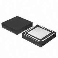
RHB Package
SN65LV1023A
Serializer
(Top View)
DGND
DVCC
DVCC
AVCC
AGND
PWRDN
AGND
DO+
DO−
AGND
DEN
AGND
AVCC
DGND
DGND
DVCC
1
28
2
27
3
26
4
25
5
24
6
23
7 DB Package 22
SN65LV1023A
8
21
Serializer
9
20
10
19
11
18
12
17
13
16
14
15
DIN9
SYNC1
SYNC2
DIN0
DIN1
DIN2
DIN3
DIN4
DIN5
DIN6
DIN7
DIN8
DIN9
TCLK_R/F
TCLK
DVCC
The SN65LV1023A and SN65LV1224B are
characterized for operation over ambient air
temperature of –40°C to 85°C.
Wireless Base Station
Backplane Interconnect
DSLAM
DGND
•
•
•
The device can be entered into a power-down state
when no data transfer is required. Alternatively, a
mode is available to place the output pins in the
high-impedance state without losing PLL lock.
SYNC1
•
•
DGND
•
Upon power up, the chipset link can be initialized via
a synchronization mode with internally generated
SYNC patterns or the deserializer can be allowed to
synchronize to random data. By using the
synchronization mode, the deserializer establishes
lock within specified, shorter time parameters.
SYNC2
•
•
•
•
The SN65LV1023A serializer and SN65LV1224B
deserializer comprise a 10-bit serdes chipset
designed to transmit and receive serial data over
LVDS differential backplanes at equivalent parallel
word rates from 10 MHz to 66 MHz. Including
overhead, this translates into a serial data rate
between 120-Mbps and 792-Mbps payload encoded
throughput.
TCLK
•
DESCRIPTION
DIN0
•
100-Mbps to 660-Mbps Serial LVDS Data
Payload Bandwidth at 10-MHz to 66-MHz
System Clock
Pin-Compatible Superset of
DS92LV1023/DS92LV1224
Chipset (Serializer/Deserializer) Power
Consumption 6
cycles, another 1026 SYNC pattern transmission initiates.
1, 2
30, 31
SYNC1,
SYNC2
13
10
TCLK_R/F
14
11
TCLK
LVTTL-level reference clock input. The SN65LV1023A accepts a 10-MHz to
66-MHz clock. TCLK strobes parallel data into the input latch and provides a
reference frequency to the PLL.
1, 12, 13
10, 11, 28, 29, 30
AGND
Analog circuit ground (PLL and analog circuits)
4, 11
1, 8, 9
AVCC
Analog circuit power supply (PLL and analog circuits)
14, 20, 22
12, 13, 19, 21
DGND
Digital circuit ground
21, 23
20, 22
DVCC
Digital circuit power supply
10
7
LOCK
LVTTL level output. LOCK goes low when the deserializer PLL locks onto the
embedded clock edge.
7
4
PWRDN
2
31
RCLK_R/F
9
6
RCLK
3
32
REFCLK
LVTTL logic input. Use this pin to supply a REFCLK signal for the internal PLL
frequency.
8
5
REN
LVTTL logic input. Low places ROUT0−ROUT9 and RCLK in the high-impedance
state.
5
2
RI+
Serial data input. Noninverting LVDS differential input
6
3
RI–
Serial data input. Inverting LVDS differential input
28−24, 19−15
27−23, 18−14
ROUT0−ROUT9
LVTTL logic input. Low selects a TCLK falling-edge data strobe; high selects a
TCLK rising-edge data strobe.
DESERIALIZER
6
Submit Documentation Feedback
LVTTL logic input. Asserting this pin low turns off the PLL and places outputs into a
high-impedance state, putting the device into a low-power mode. To initiate power
down, this pin is held low for a minimum of 16 ns. As long as PWRDN is held low,
the device is in the power down state.
LVTTL logic input. Low selects an RCLK falling-edge data strobe; high selects an
RCLK rising-edge data strobe.
LVTTL level output recovered clock. Use RCLK to strobe ROUTx.
Parallel LVTTL data outputs
Copyright © 2004–2009, Texas Instruments Incorporated
Product Folder Link(s): SN65LV1023A SN65LV1224B
�SN65LV1023A
SN65LV1224B
www.ti.com
SLLS621E – SEPTEMBER 2004 – REVISED DECEMBER 2009
ABSOLUTE MAXIMUM RATINGS
over operating free-air temperature range (unless otherwise noted) (1)
UNIT
−0.3 V to 4 V
VCC to GND
LVTTL input voltage
−0.3 V to (VCC + 0.3 V)
LVTTL output voltage
−0.3 V to (VCC + 0.3 V)
LVDS receiver input voltage
−0.3 V to 3.9 V
LVDS driver output voltage
−0.3 V to 3.9 V
LVDS output short circuit duration
Electrostatic discharge:
10 ms
HBM
up to 6 kV
MM
up to 200 V
Junction temperature
150°C
−65°C to 150°C
Storage temperature
DB package maximum package
power dissipation
TA = 25°C
1.27 W
RHB package maximum package TA = 25°C
power dissipation
2.85 W
DB package derating
10.3 mW/°C above 25°C
RHB package derating
23.6 mW/°C above 25°C
(1)
Stresses beyond those listed under absolute maximum ratings may cause permanent damage to the device. These are stress ratings
only, and functional operation of the device at these or any other conditions beyond those indicated under recommended operating
conditions is not implied. Exposure to absolute-maximum-rated conditions for extended periods may affect device reliability.
RECOMMENDED OPERATING CONDITIONS
over operating free-air temperature range (unless otherwise noted)
VCC
(1)
MIN
NOM
MAX
Supply voltage
3
3.3
3.6
V
Receiver input voltage range
0
2.4
V
ID
2
ǒ Ǔ
V
V
VCM
Receiver input common mode range
V
2.4 *
Supply noise voltage
TA
(1)
ID
2
100
Operating free-air temperature
–40
UNIT
mVPP
25
°C
By design, DVCC and AVCC are separated internally and does not matter what the difference is for |DVCC−AVCC|, as long as both are
within 3 V to 3.6 V.
Copyright © 2004–2009, Texas Instruments Incorporated
Product Folder Link(s): SN65LV1023A SN65LV1224B
Submit Documentation Feedback
7
�SN65LV1023A
SN65LV1224B
SLLS621E – SEPTEMBER 2004 – REVISED DECEMBER 2009
www.ti.com
ELECTRICAL CHARACTERISTICS
over recommended operating supply and temperature ranges (unless otherwise specified)
PARAMETER
TEST CONDITIONS
MIN
TYP
MAX
UNIT
SERIALIZER LVCMOS/LVTTL DC SPECIFICATIONS (1)
VIH
High-level input voltage
2
VCC
V
VIL
Low-level input voltage
GND
0.8
V
VCL
Input clamp voltage
IIN
Input current,
ICL = −18 mA
(2)
VIN = 0 V or 3.6 V
–200
-0.86
–1.5
V
±100
200
μA
DESERIALIZER LVCMOS/LVTTL DC SPECIFICATIONS (3)
VIH
High-level input voltage
2
VCC
V
VIL
Low-level input voltage
GND
0.8
V
VCL
Input clamp voltage
ICL = −18 mA
–1.5
V
IIN
Input current (pull-up and
pull-down resistors on inputs)
VIN = 0 V or 3.6 V
200
μA
VOH
High-level output voltage
IOH = −5 mA
2.2
3
VCC
V
VOL
Low-level output voltage
IOL = 5 mA
GND
0.25
0.5
V
IOS
Output short-circuit current
VOUT = 0 V
–15
–47
–85
mA
IOZ
High-impedance output current
PWRDN or REN = 0.8 V, VOUT = 0 V or VCC
–10
±1
10
μA
350
450
-0.62
–200
SERIALIZER LVDS DC SPECIFICATIONS (Apply to Pins DO+ and DO−)
VOD
Output differential voltage
(DO+)–(DO−)
ΔVOD
Output differential voltage
unbalance
VOS
Offset voltage
ΔVOS
Offset voltage unbalance
IOS
Output short circuit current
D0 = 0 V, DINx = high,
PWRDN and DEN = 2.4 V
IOZ
High-impedance output current
PWRDN or DEN = 0.8 V,
DO = 0 V or VCC
–10
IOX
Power-off output current
VCC = 0 V, DO = 0 V or 3.6 V
-20
CO
Output single-ended capacitance
RL = 27 Ω, See Figure 2
mV
35
1.1
mV
1.2
1.3
V
4.8
35
mV
-10
-90
mA
±1
10
μA
±1
25
μA
1±20%
pF
50
mV
DESERIALIZER LVDS DC SPECIFICATIONS (Apply to Pins RI+ and RI−)
VTH
Differential threshold high voltage
VTL
Differential threshold low voltage
IIN
Input current
CI
Input single-ended capacitance
VCM = 1.1 V
–50
mV
VIN = 2.4 V, VCC = 3.6 V or 0 V
–10
±1
15
VIN = 0 V, VCC = 3.6 V or 0 V
–10
±0.05
10
0.5±20%
μA
pF
SERIALIZER SUPPLY CURRENT (Applies to Pins DVCC and AVCC)
ICCD
Serializer supply current worst
case
RL = 27 Ω, See Figure 5
ICCXD
Serializer supply current
PWRDN = 0.8 V
f = 10 MHz
20
25
f = 66 MHz
55
70
200
500
f = 10 MHz
15
35
f = 66 MHz
80
95
0.36
1
mA
μA
DESERIALIZER SUPPLY CURRENT (applies to pins DVCC and AVCC)
ICCR
Deserializer supply current, worst
case
CL = 15 pF, See Figure 5
ICCXR
Deserializer supply current, power
down
PWRDN = 0.8 V, REN = 0.8 V
(1)
(2)
(3)
8
mA
mA
Apply to DIN0−DIN9, TCLK, PWRDN, TCLK_R/F, SYNC1, SYNC2, and DEN
High IIN values are due to pullup and pulldown resistors on the inputs.
Apply to pins PWRDN, RCLK_R/F, REN, and REFCLK = inputs; apply to pins ROUTx, RCLK, and LOCK = outputs
Submit Documentation Feedback
Copyright © 2004–2009, Texas Instruments Incorporated
Product Folder Link(s): SN65LV1023A SN65LV1224B
�SN65LV1023A
SN65LV1224B
www.ti.com
SLLS621E – SEPTEMBER 2004 – REVISED DECEMBER 2009
1000
900
800
VOD
VOD IN - mV
700
600
500
400
300
200
100
0
0
20
40
60
80
100
120
140
Termination (RL) - W
Figure 2. Typical VOD Curve
SERIALIZER TIMING REQUIREMENTS FOR TCLK
over recommended operating supply and temperature ranges (unless otherwise specified)
PARAMETER
MIN
TYP
MAX
UNIT
15.15
T
100
ns
Transmit clock high time
0.4T
0.5T
0.6T
ns
tTCIL
Transmit clock low time
0.4T
0.5T
0.6T
ns
tt(CLK)
TCLK input transition time
3
6
tJIT
TCLK input jitter
tTCP
Transmit clock period
tTCIH
TEST CONDITIONS
See Figure 19
Frequency tolerance
-100
Copyright © 2004–2009, Texas Instruments Incorporated
Product Folder Link(s): SN65LV1023A SN65LV1224B
ns
150
ps (RMS)
+100
ppm
Submit Documentation Feedback
9
�SN65LV1023A
SN65LV1224B
SLLS621E – SEPTEMBER 2004 – REVISED DECEMBER 2009
www.ti.com
SERIALIZER SWITCHING CHARACTERISTICS
over recommended operating supply and temperature ranges (unless otherwise specified)
PARAMETER
TEST CONDITIONS
tTLH(L)
LVDS low-to-high transition time
tLTHL(L)
LVDS high-to-low transition time
tsu(DI)
DIN0−DIN9 setup to TCLK
tsu(DI)
DIN0−DIN9 hold from TCLK
td(HZ)
DO± high-to-high impedance state
delay
td(LZ)
DO± low-to-high impedance state
delay
td(ZH)
DO± high-to-high impedance
state-to-high delay
td(ZL)
DO± high-to-high impedance
state-to-low delay
tw(SPW)
SYNC pulse duration
t(PLD)
Serializer PLL lock time
td(S)
Serializer delay
MIN
RL = 27 Ω, CL = 10 pF to GND, See
Figure 6
tDJIT
Deterministic jitter
RL = 27 Ω, CL = 10 pF to GND
tRJIT
Random jitter
RL = 27 Ω, CL = 10 pF to GND
0.4
ns
0.25
0.4
ns
ns
2.5
5
2.5
5
5
10
6.5
10
6×tTCP
ns
ns
1026×tTCP
tTCP+1
UNIT
ns
4
RL = 27 Ω, CL = 10 pF to GND, See
Figure 10
See Figure 13
MAX
0.2
0.5
See Figure 9
See Figure 12
TYP
ns
tTCP+2
tTCP+3
230
150
10
19
ns
ps
ps (RMS)
DESERIALIZER TIMING REQUIREMENTS FOR REFCLK
over recommended operating supply and temperature ranges (unless otherwise specified)
PARAMETER
tRFCP
REFCLK period
tRFDC
REFCLK duty cycle
tt(RF)
REFCLK transition time
Frequency tolerance
10
Submit Documentation Feedback
TEST CONDITIONS
MIN
TYP
MAX
UNIT
15.15
T
100
ns
30%
50%
70%
3
-100
6
+100
ns
ppm
Copyright © 2004–2009, Texas Instruments Incorporated
Product Folder Link(s): SN65LV1023A SN65LV1224B
�SN65LV1023A
SN65LV1224B
www.ti.com
SLLS621E – SEPTEMBER 2004 – REVISED DECEMBER 2009
DESERIALIZER SWITCHING CHARACTERISTICS
over recommended operating supply and temperature ranges (unless otherwise specified)
PARAMETER
t(RCP)
Receiver out clock period
tTLH(C)
CMOS/TTL low-to-high
transition time
tTHL(C)
CMOS/TTL high-to-low
transition time
td(D)
Deserializer delay, See
Figure 14
t(ROS)
TEST
CONDITIONS
t(RCP) = t(TCP), See
Figure 13
CL = 15 pF, CL =
15 pF, See
Figure 7
Room temperature,
3.3 V
ROUTx data valid before RCLK
See Figure 15
PIN/FREQ
RCLK
MIN
TYP
15.15
ROUT0−ROUT9
LOCK, RCLK
MAX
UNIT
100
ns
1.2
2.5
1.1
2.5
ns
10 MHz
1.75×t(RCP)
+4.2
1.75×t(RCP)
+12.6
ns
66 MHz
1.75×t(RCP)
+7.4
1.75×t(RCP)
+9.7
ns
RCLK 10 MHz
0.4×t(RCP)
RCLK 66 MHz
0.4×t(RCP)
0.5×t(RCP)
0.5×t(RCP)
10 MHz
−0.4×t(RCP)
−0.5×t(RCP)
66 MHz
−0.4×t(RCP)
−0.5×t(RCP)
40%
ns
t(ROH)
ROUTx data valid after RCLK
t(RDC)
RCLK duty cycle
50%
60%
ns
td(HZ)
High-to-high impedance state
delay
6.5
8
ns
td(LZ)
Low-to-high impedance state
delay
4.7
8
ns
td(HR)
High-impedance state to high
delay
5.3
8
ns
td(ZL)
High-impedance state to low
delay
4.7
8
ns
t(DSR1)
Deserializer PLL lock time from
PWRDN (with SYNCPAT)
t(DSR2)
Deserializer PLL lock time from
SYNCPAT
td(ZHLK)
High-impedance state to high
delay (power up)
tRNM
Deserializer noise margin
(1)
(2)
See Figure 16
See Figure 17,
Figure 18,
and (1)
ROUT0−ROUT9
10 MHz
850 x tRFCP
66 MHz
850 x tRFCP
10 MHz
2
66 MHz
0.303
LOCK
See Figure 19 and
(2)
3
10 MHz
3680
66 MHz
540
μs
ns
ps
t(DSR1) represents the time required for the deserializer to register that a lock has occurred upon powerup or when leaving the
powerdown mode. t(DSR2) represents the time required to register that a lock has occurred for the powered up and enabled deserializer
when the input (RI±) conditions change from not receiving data to receiving synchronization patterns (SYNCPATs). In order to specify
deserializer PLL performance, tDSR1 and tDSR2 are specified with REFCLK active and stable and specific conditions of SYNCPATs.
tRNM represents the phase noise or jitter that the deserializer can withstand in the incoming data stream before bit errors occur.
Copyright © 2004–2009, Texas Instruments Incorporated
Product Folder Link(s): SN65LV1023A SN65LV1224B
Submit Documentation Feedback
11
�SN65LV1023A
SN65LV1224B
SLLS621E – SEPTEMBER 2004 – REVISED DECEMBER 2009
www.ti.com
TIMING DIAGRAMS AND TEST CIRCUITS
TCLK
ODD DIN
EVEN DIN
Figure 3. Worst-Case Serializer ICC Test Pattern
SUPPLY CURRENT
vs
TCLK FREQUENCY
60
66 MHz, 48.88 mA
ICC − Supply Current − mA
50
40
ICC
30
20
10 MHz, 14.732 mA
10
0
0
20
40
60
80
TCLK Frequency − MHz
Figure 4.
12
Submit Documentation Feedback
Copyright © 2004–2009, Texas Instruments Incorporated
Product Folder Link(s): SN65LV1023A SN65LV1224B
�SN65LV1023A
SN65LV1224B
www.ti.com
SLLS621E – SEPTEMBER 2004 – REVISED DECEMBER 2009
RCLK
ODD ROUT
EVEN ROUT
Figure 5. Worst-Case Deserializer ICC Test Pattern
10 pF
tTLH(L)
DO+
RL
tTHL(L)
80%
Vdiff
80%
20%
20%
DO−
10 pF
Vdiff = (DO+) − (DO−)
Figure 6. Serializer LVDS Output Load and Transition Times
CMOS/TTL Output
Deserializer
tTHL(C)
tTLH(C)
80%
15 pF
80%
20%
20%
Figure 7. Deserializer CMOS/TTL Output Load and Transition Times
tt(CLK)
TCLK
tt(CLK)
90%
10%
90%
10%
3V
0V
Figure 8. Serializer Input Clock Transition Time
Copyright © 2004–2009, Texas Instruments Incorporated
Product Folder Link(s): SN65LV1023A SN65LV1224B
Submit Documentation Feedback
13
�SN65LV1023A
SN65LV1224B
SLLS621E – SEPTEMBER 2004 – REVISED DECEMBER 2009
www.ti.com
tTCP
1.5 V
TCLK
1.5 V
1.5 V
For TCLK_R/F = Low
th(DI)
tsu(DI)
DIN [9:0]
1.5 V
Setup
Hold
1.5 V
Figure 9. Serializer Setup/Hold Times
Parasitic Package and
Trace Capacitance
3V
DEN
1.5 V
1.5 V
0V
td(ZH)
td(HZ)
VOH
13.5 Ω
DO+
50%
1.1 V
DO−
DO±
50%
1.1 V
td(ZL)
td(LZ)
13.5 Ω
DEN
1.1 V
50%
50%
VOL
Figure 10. Serializer High-Impedance State Test Circuit and Timing
PWRDN
2V
0.8 V
1026 Cycles
td(HZ) or td(LZ)
TCLK
td(ZH) or td(ZL)
tPLD
DO±
3-State
Output Active
3-State
Figure 11. Serializer PLL Lock Time and PWRDN High-Impedance State Delays
14
Submit Documentation Feedback
Copyright © 2004–2009, Texas Instruments Incorporated
Product Folder Link(s): SN65LV1023A SN65LV1224B
�SN65LV1023A
SN65LV1224B
www.ti.com
SLLS621E – SEPTEMBER 2004 – REVISED DECEMBER 2009
REN
PWRDN
TCLK
tw(SP)
SYNC1
or
SYNC2
DO±
DATA
SYNC Pattern
TCLK
SYNC1
or
SYNC2
tw(SP) Min. Timing Met
DO±
SYNC Pattern
DATA
Figure 12. SYNC Timing Delays
DIN
DIN0 − DIN9 SYMBOL N
DIN0 − DIN9 SYMBOL N+1
td(S)
TCLK
Timing for TCLK_R/F = High
Start
D00 − D09 SYMBOL N−1
Bit
Stop Start
Bit Bit
D00 − D09 SYMBOL N
Stop
Bit
DO
Figure 13. Serializer Delay
Copyright © 2004–2009, Texas Instruments Incorporated
Product Folder Link(s): SN65LV1023A SN65LV1224B
Submit Documentation Feedback
15
�SN65LV1023A
SN65LV1224B
SLLS621E – SEPTEMBER 2004 – REVISED DECEMBER 2009
Start
Bit
www.ti.com
Stop Start
Bit Bit
D00 − D09 SYMBOL N
D00 − D09 SYMBOL N+1
Stop Start
Bit Bit
D00 − D09 SYMBOL N+2
Stop
Bit
RI
1.2 V
1V
tDD
RCLK
Timing for TCLK_R/F = High
ROUT
ROUT0 − ROUT9 SYMBOL N−1
ROUT0 − ROUT9 SYMBOL N
ROUT0 − ROUT9 SYMBOL N+1
Figure 14. Deserializer Delay
tLow
tHigh
RCLK
RCLK_R/F = Low
tHigh
tLow
RCLK
RCLK_R/F = High
tROH
tROS
ROUT [9:0]
1.5 V
Data Valid
Before RCLK
Data Valid
After RCLK
1.5 V
Figure 15. Deserializer Data Valid Out Times
7 V x (LZ/ZL), Open (HZ/ZH)
VOH
REN
500 Ω
450 Ω
1.5 V
1.5 V
VOL
Scope
td(LZ)
VOL + 0.5 V
50 Ω
td(ZL)
VOL + 0.5 V
VOL
ROUT[9:0]
td(HZ)
td(ZH)
VOH
VOH − 0.5 V
VOH − 0.5 V
Figure 16. Deserializer High-Impedance State Test Circuit and Timing
16
Submit Documentation Feedback
Copyright © 2004–2009, Texas Instruments Incorporated
Product Folder Link(s): SN65LV1023A SN65LV1224B
�SN65LV1023A
SN65LV1224B
www.ti.com
PWRDN
SLLS621E – SEPTEMBER 2004 – REVISED DECEMBER 2009
2V
0.8 V
REFCLK
1.5 V
t(DSR1)
DATA
RI±
Not Important
td(ZHL)
LOCK
SYNC Patterns
3-State
3-State
td(ZH) or td(ZL)
ROUT[9:0]
td(HZ) or td(LZ)
3-State
3-State
SYNC Symbol or DIN[9:0]
RCLK
3-State
3-State
RCLK_R/F = Low
REN
Figure 17. Deserializer PLL Lock Times and PWRDN 3-State Delays
Copyright © 2004–2009, Texas Instruments Incorporated
Product Folder Link(s): SN65LV1023A SN65LV1224B
Submit Documentation Feedback
17
�SN65LV1023A
SN65LV1224B
SLLS621E – SEPTEMBER 2004 – REVISED DECEMBER 2009
www.ti.com
3.6 V
3V
VCC
0V
PWRDN
0.8 V
REFCLK
t(DSR2)
DATA
1.2 V
RI±
Not Important
1V
SYNC Patterns
LOCK
3-State
td(ZH) or td(ZL)
ROUT[9:0]
td(HZ) or td(LZ)
3-State
3-State
SYNC Symbol or DIN[9:0]
RCLK
3-State
3-State
REN
Figure 18. Deserializer PLL Lock Time From SyncPAT
1.2 V
VTH
RI±
VTL
1V
tDJIT
tDJIT
tRNM
tRNM
tSW
Ideal Sampling Position
tSW: Setup and Hold Time (Internal Data Sampling Window)
tDJIT: Serializer Output Bit Position Jitter That Results From Jitter on TCLK
tRNM: Receiver Noise Margin Time
Figure 19. Receiver LVDS Input Skew Margin
18
Submit Documentation Feedback
Copyright © 2004–2009, Texas Instruments Incorporated
Product Folder Link(s): SN65LV1023A SN65LV1224B
�SN65LV1023A
SN65LV1224B
www.ti.com
SLLS621E – SEPTEMBER 2004 – REVISED DECEMBER 2009
DO+
RL
10
Parallel-to-Serial
DIN
DO−
> TCLK
VOD = (DO+) − (DO−)
Differential Output Signal Is Shown as (DO+) − (DO−)
Figure 20. VOD Diagram
DEVICE STARTUP PROCEDURE
It is recommended that the PWRDNB pin on both the SN65LV1023A and the SN65LV1224B device be held to a
logic LOW level until after the power supplies have powered up to at least 3 V as shown in Figure 21.
3.0 V
VDD
PWRDNB
Figure 21. Device Startup
Copyright © 2004–2009, Texas Instruments Incorporated
Product Folder Link(s): SN65LV1023A SN65LV1224B
Submit Documentation Feedback
19
�SN65LV1023A
SN65LV1224B
SLLS621E – SEPTEMBER 2004 – REVISED DECEMBER 2009
www.ti.com
APPLICATION INFORMATION
DIFFERENTIAL TRACES AND TERMINATION
The performance of the SN65LV1023A/SN65LV1224B is affected by the characteristics of the transmission
medium. Use controlled-impedance media and termination at the receiving end of the transmission line with the
media’s characteristics impedance.
Use balanced cables such as twisted pair or differential traces that are ran close together. A balanced cable
picks up noise together and appears to the receiver as common mode. Differential receivers reject
common-mode noise. Keep cables or traces matched in length to help reduce skew.
Running the differential traces close together helps cancel the external magnetic field, as well as maintain a
constant impedance. Avoiding sharp turns and reducing the number of vias also helps.
TOPOLOGIES
There are several topologies that the serializers can operate. Three common examples are shown below.
Figure 22 shows an example of a single-terminated point-to-point connection. Here a single termination resistor
is located at the deserializer end. The resistor value should match that of the characteristic impedance of the
cable or PC board traces. The total load seen by the serializer is 100 Ω. Double termination can be used and
typically reduces reflections compared with single termination. However, it also reduces the differential output
voltage swing.
AC-coupling is only recommended if the parallel TX data stream is encoded to achieve a dc-balanced data
stream. Otherwise the ac-capacitors can induce common mode voltage drift due to the dc-unbalanced data
stream.
Serialized Data
100 Ω
Parallel Data In
Parallel Data Out
Figure 22. Single-Terminated Point-to-Point Connection
Figure 23 shows an example of a multidrop configuration. Here there is one transmitter broadcasting data to
multiple receivers. A 50-kΩ resistor at the far end terminates the bus.
ASIC
ASIC
ASIC
ASIC
50 Ω
Figure 23. Multidrop Configuration
Figure 24 shows an example of multiple serializers and deserializers on the same differential bus, such as in a
backplane. This is a multipoint configuration. In this situation, the characteristic impedance of the bus can be
significantly less due to loading. Termination resistors that match the loaded characteristic impedance are
required at each end of the bus. The total load seen by the serializer in this example is 27 Ω.
20
Submit Documentation Feedback
Copyright © 2004–2009, Texas Instruments Incorporated
Product Folder Link(s): SN65LV1023A SN65LV1224B
�SN65LV1023A
SN65LV1224B
www.ti.com
SLLS621E – SEPTEMBER 2004 – REVISED DECEMBER 2009
ASIC
ASIC
ASIC
ASIC
54 Ω
54 Ω
Figure 24. Multiple Serializers and Deserializers on the Same Differential Bus
SPACER
REVISION HISTORY
Changes from Original (September 2004) to Revision A
Page
•
Changed Figure 17 ............................................................................................................................................................. 17
•
Changed Figure 18 ............................................................................................................................................................. 18
Changes from Revision A (January 2005) to Revision B
•
Page
Added RHB package information ......................................................................................................................................... 1
Changes from Revision B (July 2005) to Revision C
•
Page
Changed Package description in the Features list. .............................................................................................................. 1
Changes from Revision C (February 2006) to Revision D
Page
•
Added the Applications List .................................................................................................................................................. 1
•
Deleted the DB and RHB packages for Deserializer ............................................................................................................ 1
•
Added Figure 2 ..................................................................................................................................................................... 9
•
Changed Figure 4 Supply Current vs TCLK Frequency ..................................................................................................... 12
Changes from Revision D (February 2009) to Revision E
•
Page
Deleted footnote - "The deserializer delay time for all frequencies does not exceed two serial bit times" From td(D) ........ 11
Copyright © 2004–2009, Texas Instruments Incorporated
Product Folder Link(s): SN65LV1023A SN65LV1224B
Submit Documentation Feedback
21
�PACKAGE OPTION ADDENDUM
www.ti.com
14-Oct-2022
PACKAGING INFORMATION
Orderable Device
Status
(1)
Package Type Package Pins Package
Drawing
Qty
Eco Plan
(2)
Lead finish/
Ball material
MSL Peak Temp
Op Temp (°C)
Device Marking
(3)
Samples
(4/5)
(6)
SN65LV1023ADB
ACTIVE
SSOP
DB
28
50
RoHS & Green
NIPDAU
Level-1-260C-UNLIM
-40 to 85
LV1023A
Samples
SN65LV1023ADBR
ACTIVE
SSOP
DB
28
2000
RoHS & Green
NIPDAU
Level-1-260C-UNLIM
-40 to 85
LV1023A
Samples
SN65LV1023ARHBR
ACTIVE
VQFN
RHB
32
3000
RoHS & Green
NIPDAU
Level-2-260C-1 YEAR
-40 to 85
SN65LV
1023A
Samples
SN65LV1023ARHBT
ACTIVE
VQFN
RHB
32
250
RoHS & Green
NIPDAU
Level-2-260C-1 YEAR
-40 to 85
SN65LV
1023A
Samples
SN65LV1224BDB
ACTIVE
SSOP
DB
28
50
RoHS & Green
NIPDAU
Level-1-260C-UNLIM
-40 to 85
LV1224B
Samples
SN65LV1224BDBG4
ACTIVE
SSOP
DB
28
50
RoHS & Green
NIPDAU
Level-1-260C-UNLIM
-40 to 85
LV1224B
Samples
SN65LV1224BDBR
ACTIVE
SSOP
DB
28
2000
RoHS & Green
NIPDAU
Level-1-260C-UNLIM
-40 to 85
LV1224B
Samples
SN65LV1224BRHBR
ACTIVE
VQFN
RHB
32
3000
RoHS & Green
NIPDAU
Level-2-260C-1 YEAR
-40 to 85
SN65LV
1224B
Samples
SN65LV1224BRHBT
ACTIVE
VQFN
RHB
32
250
RoHS & Green
NIPDAU
Level-2-260C-1 YEAR
-40 to 85
SN65LV
1224B
Samples
(1)
The marketing status values are defined as follows:
ACTIVE: Product device recommended for new designs.
LIFEBUY: TI has announced that the device will be discontinued, and a lifetime-buy period is in effect.
NRND: Not recommended for new designs. Device is in production to support existing customers, but TI does not recommend using this part in a new design.
PREVIEW: Device has been announced but is not in production. Samples may or may not be available.
OBSOLETE: TI has discontinued the production of the device.
(2)
RoHS: TI defines "RoHS" to mean semiconductor products that are compliant with the current EU RoHS requirements for all 10 RoHS substances, including the requirement that RoHS substance
do not exceed 0.1% by weight in homogeneous materials. Where designed to be soldered at high temperatures, "RoHS" products are suitable for use in specified lead-free processes. TI may
reference these types of products as "Pb-Free".
RoHS Exempt: TI defines "RoHS Exempt" to mean products that contain lead but are compliant with EU RoHS pursuant to a specific EU RoHS exemption.
Green: TI defines "Green" to mean the content of Chlorine (Cl) and Bromine (Br) based flame retardants meet JS709B low halogen requirements of


 工商网监
湘ICP备2023018690号
工商网监
湘ICP备2023018690号
