��������
� ��
User’s Guide
June 2003
HPL Interface
SLLU060
�IMPORTANT NOTICE
Texas Instruments Incorporated and its subsidiaries (TI) reserve the right to make corrections, modifications,
enhancements, improvements, and other changes to its products and services at any time and to discontinue
any product or service without notice. Customers should obtain the latest relevant information before placing
orders and should verify that such information is current and complete. All products are sold subject to TI’s terms
and conditions of sale supplied at the time of order acknowledgment.
TI warrants performance of its hardware products to the specifications applicable at the time of sale in
accordance with TI’s standard warranty. Testing and other quality control techniques are used to the extent TI
deems necessary to support this warranty. Except where mandated by government requirements, testing of all
parameters of each product is not necessarily performed.
TI assumes no liability for applications assistance or customer product design. Customers are responsible for
their products and applications using TI components. To minimize the risks associated with customer products
and applications, customers should provide adequate design and operating safeguards.
TI does not warrant or represent that any license, either express or implied, is granted under any TI patent right,
copyright, mask work right, or other TI intellectual property right relating to any combination, machine, or process
in which TI products or services are used. Information published by TI regarding third–party products or services
does not constitute a license from TI to use such products or services or a warranty or endorsement thereof.
Use of such information may require a license from a third party under the patents or other intellectual property
of the third party, or a license from TI under the patents or other intellectual property of TI.
Reproduction of information in TI data books or data sheets is permissible only if reproduction is without
alteration and is accompanied by all associated warranties, conditions, limitations, and notices. Reproduction
of this information with alteration is an unfair and deceptive business practice. TI is not responsible or liable for
such altered documentation.
Resale of TI products or services with statements different from or beyond the parameters stated by TI for that
product or service voids all express and any implied warranties for the associated TI product or service and
is an unfair and deceptive business practice. TI is not responsible or liable for any such statements.
Following are URLs where you can obtain information on other Texas Instruments products & application
solutions:
Products
Applications
Amplifiers
amplifier.ti.com
Audio
www.ti.com/audio
Data Converters
dataconverter.ti.com
Automotive
www.ti.com/automotive
DSP
dsp.ti.com
Broadband
www.ti.com/broadband
Interface
interface.ti.com
Digital Control
www.ti.com/digitalcontrol
Logic
logic.ti.com
Military
www.ti.com/military
Power Mgmt
power.ti.com
Optical Networking
www.ti.com/opticalnetwork
Microcontrollers
microcontroller.ti.com
Security
www.ti.com/security
Telephony
www.ti.com/telephony
Video & Imaging
www.ti.com/video
Wireless
www.ti.com/wireless
Mailing Address:
Texas Instruments
Post Office Box 655303 Dallas, Texas 75265
Copyright 2003, Texas Instruments Incorporated
�EVM IMPORTANT NOTICE
Texas Instruments (TI) provides the enclosed product(s) under the following conditions:
This evaluation kit being sold by TI is intended for use for ENGINEERING DEVELOPMENT OR EVALUATION
PURPOSES ONLY and is not considered by TI to be fit for commercial use. As such, the goods being provided
may not be complete in terms of required design-, marketing-, and/or manufacturing-related protective
considerations, including product safety measures typically found in the end product incorporating the goods.
As a prototype, this product does not fall within the scope of the European Union directive on electromagnetic
compatibility and therefore may not meet the technical requirements of the directive.
Should this evaluation kit not meet the specifications indicated in the EVM User’s Guide, the kit may be returned
within 30 days from the date of delivery for a full refund. THE FOREGOING WARRANTY IS THE EXCLUSIVE
WARRANTY MADE BY SELLER TO BUYER AND IS IN LIEU OF ALL OTHER WARRANTIES, EXPRESSED,
IMPLIED, OR STATUTORY, INCLUDING ANY WARRANTY OF MERCHANTABILITY OR FITNESS FOR ANY
PARTICULAR PURPOSE.
The user assumes all responsibility and liability for proper and safe handling of the goods. Further, the user
indemnifies TI from all claims arising from the handling or use of the goods. Please be aware that the products
received may not be regulatory compliant or agency certified (FCC, UL, CE, etc.). Due to the open construction
of the product, it is the user’s responsibility to take any and all appropriate precautions with regard to electrostatic
discharge.
EXCEPT TO THE EXTENT OF THE INDEMNITY SET FORTH ABOVE, NEITHER PARTY SHALL BE LIABLE
TO THE OTHER FOR ANY INDIRECT, SPECIAL, INCIDENTAL, OR CONSEQUENTIAL DAMAGES.
TI currently deals with a variety of customers for products, and therefore our arrangement with the user is not
exclusive.
TI assumes no liability for applications assistance, customer product design, software performance, or
infringement of patents or services described herein.
Please read the EVM User’s Guide and, specifically, the EVM Warnings and Restrictions notice in the EVM
User’s Guide prior to handling the product. This notice contains important safety information about temperatures
and voltages. For further safety concerns, please contact the TI application engineer.
Persons handling the product must have electronics training and observe good laboratory practice standards.
No license is granted under any patent right or other intellectual property right of TI covering or relating to any
machine, process, or combination in which such TI products or services might be or are used.
Mailing Address:
Texas Instruments
Post Office Box 655303
Dallas, Texas 75265
Copyright 2003, Texas Instruments Incorporated
�EVM WARNINGS AND RESTRICTIONS
It is important to operate this EVM within the input voltage range between 1.2 V and 3.3 V.
Exceeding the specified input range may cause unexpected operation and/or irreversible
damage to the EVM. If there are questions concerning the input range, please contact a TI
field representative prior to connecting the input power.
Applying loads outside of the specified output range may result in unintended operation and/or
possible permanent damage to the EVM. Please consult the EVM User’s Guide prior to
connecting any load to the EVM output. If there is uncertainty as to the load specification,
please contact a TI field representative.
During normal operation, some circuit components may have case temperatures greater than
60°C. The EVM is designed to operate properly with certain components above 60°C as long
as the input and output ranges are maintained. These components include but are not limited
to linear regulators, switching transistors, pass transistors, and current sense resistors. These
types of devices can be identified using the EVM schematic located in the EVM User’s Guide.
When placing measurement probes near these devices during operation, please be aware
that these devices may be very warm to the touch.
Mailing Address:
Texas Instruments
Post Office Box 655303
Dallas, Texas 75265
Copyright 2003, Texas Instruments Incorporated
�Trademarks
Preface
�������� �
�� �
About This Manual
This user’s guide describes the SN65LVCP22/23 evaluation module (EVM).
This guide contains the EVM schematic, bill of materials, assembly drawing,
and board layouts.
How to Use This Manual
This document contains the following chapters:
- Chapter 1– Introduction
- Chapter 2– Setup and Equipment Required
- Chapter 3– EVM Construction
- Chapter 4– PCB Fabrication and Bill of Materials
This user’s guide may contain cautions and warnings. The information in a
caution or a warning is provided for your protection. Please read each caution
and warning carefully.
Related Documentation From Texas Instruments
SN65LVCP22 – LVDS crosspoint switch data sheet (SLLS553)
SN65LVCP23 – LVPECL crosspoint switch data sheet (SLLS554)
Trademarks
Trademarks are the property of their respective owners.
v
�Trademarks
Electrostatic Sensitive Devices
This EVM contains components that can potentially be damaged by
electrostatic discharge. Always transport and store the EVM in its
supplied ESD bag when not in use. Handle using an antistatic
wristband. Operate on an antistatic work surface. For more
information on proper handling, refer to SSYA008.
vi
�Contents
������
1
Introduction . . . . . . . . . . . . . . . . . . . . . . . . . . . . . . . . . . . . . . . . . . . . . . . . . . . . . . . . . . . . . . . . . . . . . 1-1
1.1
Overview . . . . . . . . . . . . . . . . . . . . . . . . . . . . . . . . . . . . . . . . . . . . . . . . . . . . . . . . . . . . . . . . . . 1-2
1.2
Signal Paths . . . . . . . . . . . . . . . . . . . . . . . . . . . . . . . . . . . . . . . . . . . . . . . . . . . . . . . . . . . . . . . 1-3
2
Setup and Equipment Required . . . . . . . . . . . . . . . . . . . . . . . . . . . . . . . . . . . . . . . . . . . . . . . . . . .
2.1
Overview . . . . . . . . . . . . . . . . . . . . . . . . . . . . . . . . . . . . . . . . . . . . . . . . . . . . . . . . . . . . . . . . . .
2.2
Applying an Input . . . . . . . . . . . . . . . . . . . . . . . . . . . . . . . . . . . . . . . . . . . . . . . . . . . . . . . . . . .
2.3
Observing an Output . . . . . . . . . . . . . . . . . . . . . . . . . . . . . . . . . . . . . . . . . . . . . . . . . . . . . . . .
2.4
Typical Test Results . . . . . . . . . . . . . . . . . . . . . . . . . . . . . . . . . . . . . . . . . . . . . . . . . . . . . . . . .
3
EVM Construction . . . . . . . . . . . . . . . . . . . . . . . . . . . . . . . . . . . . . . . . . . . . . . . . . . . . . . . . . . . . . . . 3-1
3.1
Schematics . . . . . . . . . . . . . . . . . . . . . . . . . . . . . . . . . . . . . . . . . . . . . . . . . . . . . . . . . . . . . . . . 3-2
3.2
Board Layout Patterns . . . . . . . . . . . . . . . . . . . . . . . . . . . . . . . . . . . . . . . . . . . . . . . . . . . . . . 3-4
4
PCB Fabrication and Bill of Materials . . . . . . . . . . . . . . . . . . . . . . . . . . . . . . . . . . . . . . . . . . . . . 4-1
4.1
PCB Fabrication Notes and Stackup . . . . . . . . . . . . . . . . . . . . . . . . . . . . . . . . . . . . . . . . . . 4-2
4.2
Bill of Materials for SN65LVCP22/23 EVM . . . . . . . . . . . . . . . . . . . . . . . . . . . . . . . . . . . . . 4-2
2-1
2-2
2-3
2-4
2-5
vii
�Contents
�����
1–1
1–2
1–3
2–1
2–2
2–3
3–1
3–2
3–3
3–4
3–5
3–6
3–7
Functional Configurations of the SN65LVCP22 and SN65LVCP23 . . . . . . . . . . . . . . . . . . .
SN65LVCP22/23 EVM . . . . . . . . . . . . . . . . . . . . . . . . . . . . . . . . . . . . . . . . . . . . . . . . . . . . . . . . .
SN65LVCP22/23 EVM . . . . . . . . . . . . . . . . . . . . . . . . . . . . . . . . . . . . . . . . . . . . . . . . . . . . . . . . .
EVM Power Connections for SN65LVCP22/23 Evaluation—With LVDS Inputs . . . . . . . .
External Termination for Interfacing CML or LVPECL Drivers . . . . . . . . . . . . . . . . . . . . . . . .
Typical Test Results of the SN65LVCP23 with the SN65LVCP22/23EVM . . . . . . . . . . . . .
SN65LVCP22D Schematic . . . . . . . . . . . . . . . . . . . . . . . . . . . . . . . . . . . . . . . . . . . . . . . . . . . . .
SN65LVCP23D Schematic . . . . . . . . . . . . . . . . . . . . . . . . . . . . . . . . . . . . . . . . . . . . . . . . . . . . .
SN65LVCP22/23 Silk Screen . . . . . . . . . . . . . . . . . . . . . . . . . . . . . . . . . . . . . . . . . . . . . . . . . . .
Layer 1 – Signal Plane . . . . . . . . . . . . . . . . . . . . . . . . . . . . . . . . . . . . . . . . . . . . . . . . . . . . . . . . .
Layer 2 – GND Plane . . . . . . . . . . . . . . . . . . . . . . . . . . . . . . . . . . . . . . . . . . . . . . . . . . . . . . . . . .
Layer 3 – Split Plane (VCC/VCC01) . . . . . . . . . . . . . . . . . . . . . . . . . . . . . . . . . . . . . . . . . . . . .
Layer 4 – GND Plane . . . . . . . . . . . . . . . . . . . . . . . . . . . . . . . . . . . . . . . . . . . . . . . . . . . . . . . . . .
1-2
1-2
1-3
2-2
2-3
2-5
3-2
3-3
3-4
3-4
3-5
3-5
3-6
�����
2–1
viii
Crosspoint Function Table . . . . . . . . . . . . . . . . . . . . . . . . . . . . . . . . . . . . . . . . . . . . . . . . . . . . . . 2-4
�Chapter 1
������������
The SN65LVCP22/23 EVM highlights the high-speed performance and
functionality of the SN65LVCP22 and SN65LVCP23 2x2 crosspoint switches.
Topic
Page
1.1
Overview . . . . . . . . . . . . . . . . . . . . . . . . . . . . . . . . . . . . . . . . . . . . . . . . . . . . . 1-2
1.2
Signal Paths . . . . . . . . . . . . . . . . . . . . . . . . . . . . . . . . . . . . . . . . . . . . . . . . . . 1-3
Introduction
1-1
�Overview
1.1 Overview
The SN65LVCP22 (LVDS output) and SN65LVCP23 (LVPECL output) are
high-speed 2x2 crosspoint switches. The four different functions that these
crosspoints provide are shown in Figure 1–1. The functions of these
crosspoints are selected via pins SEL0 and SEL1. Control pins EN0 and EN1
enable or disable the outputs. The receiver has a wide input common-mode
voltage range with an ability to accept LVDS, LVPECL and CML signaling
levels.
Figure 1–1. Functional Configurations of the SN65LVCP22 and SN65LVCP23
IN0+
OUT0+
IN0+
OUT0+
IN0–
OUT0–
IN0–
OUT0–
IN1+
OUT1+
IN1+
OUT1+
IN1–
OUT1–
IN1–
2x2 Crosspoint
IN+
(1 OR 2)
IN–
OUT1–
Dual Repeater
OUT0+
IN0+
OUT0–
IN0–
MUX
1:2 Splitter
OUT1+
IN1+
OUT1–
IN1–
OUT+
(1 OR 2)
OUT–
2:1 MUX
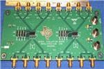
Figure 1–2 is a picture of the SN65LVCP22/23 EVM. The EVM part number
is SN65LVCP22/23EVM. The EVM comes with the SN65LVCP22D and
SN65LVCP23D (SOIC both) installed. A copy of the datasheet is shipped with
the EVM. The latest version of the datasheet is available from www.ti.com.
Figure 1–2. SN65LVCP22/23 EVM
1-2
�Signal Paths
1.2 Signal Paths
The signal paths on this EVM include 16 edge-launch SMA connectors
(J1–J16) for high-speed data transmission, 4 jumpers (JMP1, JMP2 for
DUT1and JMP5, JMP6 for DUT2) for active switch logic control, 4
jumpers (JMP3, JMP4 for DUT1and JMP7, JMP8 for DUT2) for
enabling and disabling the outputs, and three banana jacks (J17, J18,
J19) for power and ground connections. See Figure 1–3.
J10
J11
J12
J1
DUTGND
VCC01
R3
uninstalled
R4
J5
GND
68µF
1µF
68µF
1µF
0.1µF 0.1µF
0.010µF 0.010µF
10µF
10µF
C 11 DUT1
R2
J19
J18
J3
VCC
C1 C2 C3 C4 C5
J17
100 Ω
R1
0.010µF
JMP4
J2
uninstalled
R6
uninstalled
R5
R7
R8
EN0
uninstalled
uninstalled
SEL1
EN1
JMP3
JMP1
1
J9
J6
C6 C7 C8 C9 C10
100 Ω
R10
0.010µF
VCC
JMP2
R11
uninstalled
R12
SEL0
GND
100 Ω
R19
100 Ω
J7
{
C 17 DUT2
16
JMP8
JMP7
J8
1
JMP6
J13
61
VCC
1
{
GND
JMP5
uninstalled
R15
R14
uninstalled
R13
R16
J14
EN0
uninstalled
J15
EN1
SEL0
J16
SEL1
uninstalled
Figure 1–3. SN65LVCP22/23 EVM
J4
{GND is tied to Vcc01
Introduction
1-3
�1-4
�Chapter 2
����� ��� ��������� ��������
Topic
Page
2.1
Overview . . . . . . . . . . . . . . . . . . . . . . . . . . . . . . . . . . . . . . . . . . . . . . . . . . . . . 2-2
2.2
Applying an Input . . . . . . . . . . . . . . . . . . . . . . . . . . . . . . . . . . . . . . . . . . . . . 2-3
2.3
Observing an Output . . . . . . . . . . . . . . . . . . . . . . . . . . . . . . . . . . . . . . . . . . 2-4
2.4
Typical Test Results . . . . . . . . . . . . . . . . . . . . . . . . . . . . . . . . . . . . . . . . . . . 2-5
Setup and Equipment Required
2-1
�Overview
2.1 Overview
The output characteristics of the SN65LVCP23 (LVPECL) drivers are
generally loaded with 50-Ω resistors to a termination bias voltage, VTT. VTT is
usually 2 V below the supply voltage of the driver circuit. When the driver
operates from a 3.3-V supply, VTT is set to approximately 1.3 V.
The output characteristics of the SN65LVCP22 are specified in the
TIA/EIA-644 standard. LVDS drivers nominally provide a 350-mV differential
signal, with a 1.25–V offset from ground. These levels are attained when
driving a 100-W differential line-termination test load. This requirement
includes the effects of up to 32 standard receivers with their ground reference
up to 1 V different from that of the driver. This common-mode loading limitation
of LVDS drivers affects how they are observed and much of the test setup that
follows..
The EVM is designed to support the SN65LVCP22 LVDS output device as well
as the SN65LVCP23 LVPECL output device. By using the three power jacks
(J17, J18, J19), as well as installing termination resistors (R3–R8 and
R11–R16), different methods of termination and probing can be used to
evaluate the device output characteristics. The typical setup for the
SN65LVCP22 is shown in Figure 2–1.
Figure 2–1. EVM Power Connections for SN65LVCP22/23 Evaluation—With LVDS Inputs
+
Power Supply #1 3.3 V
–
+
Power Supply #2 1.2 V
–
Pattern
Generator
J19
OUTPUT 1
OUTPUT 1
J1 or J9
J2 or J10
J18
J17
GND
VCC
VCC01
(DUT GND) (EVM GND)
R1 or R19
100 Ω
J8 or J16
J7 or J15
CH1
50 Ω
CH2
50 Ω
OUTPUT 2
J3 or J11
J4 or J12
J6 or J14
R2 or R10
100 Ω
CH3
50 Ω
J5 or J13
CH4
50 Ω
OUTPUT 2
SN65LVCP22/23 EVM
Oscilloscope
2-2
�Applying an Input
2.2 Applying an Input
When using a general-purpose signal generator with 50-Ω output impedance,
make sure that the signal levels are between 0-V and 4-V with respect to J19,
device under test ground (DUT GND), designated as Vcc01.
Inputs should be applied to the SMA connectors J1, J2, J3, and J4 for DUT1
(or J9, J10, J11 and J12 for DUT2). Matched cable lengths must be used when
connecting the signal generator to the EVM to avoid inducing skew between
the noninverting and inverting inputs. The EVM comes with 100-Ω resistors
installed across the differential inputs for LVDS termination. The simple 100-Ω
terminations do not provide the necessary termination for LVPECL or CML[1]
output structures. In order to interface the SN65LVCP22/23 EVM with CML or
LVPECL drivers, external terminations are required. Figure 2–2 shows an
example termination for LVPECL and CML output structures. Remove
resistors R1, R2, R10 and R19 when using the external terminations.
Figure 2–2. External Termination for Interfacing CML or LVPECL Drivers
VTT for LVPECL
VCC for CML
50 Ω
IN+
LVPECL or CML
Driver
EVM (Inputs 1 or 2)
IN–
50 Ω
VTT for LVPECL
VCC for CML
The use of external resistors creates a significant stub between the
termination and the actual device receivers. The user needs to verify that the
transition time of the input signal, coupled with the stub length, does not lead
to reflection problems. In normal applications, the termination would be placed
as close as possible to the device inputs to minimize reflections.
The control lines SEL0 and SEL1 require LVTTL levels and are stimulated by
the Vcc power supply, via jumpers JMP1 and JMP2 (DUT1) and JMP5 and
JMP6 (DUT2). Table 2–1 shows the different functions and the control line
settings for each.
[1]CML is not a standardized physical layer and therefore the output structures and required termination differ from vendor
to vendor.
Setup and Equipment Required
2-3
�Observing an Output
Table 2–1. Crosspoint Function Table
SEL0
SEL1
OUT0
OUT1
Function
0
0
IN0
IN0
1:2 Splitter
0
1
IN0
IN1
Repeater
1
0
IN1
IN0
Switch
1
1
IN1
IN1
1:2 Splitter
2.3 Observing an Output
Direct connection to an oscilloscope with 50–Ω internal terminations to ground
is accomplished without R3–R8 (DUT1) and R11–R16 (DUT2) installed. The
outputs are available at J5–J8 (DUT1) and J13–J16 (DUT2) for direct
connection to oscilloscope inputs. Matched cable lengths must be used when
connecting the EVM to a scope to avoid inducing skew between the
noninverting (+) and inverting (–) outputs.
The three power jacks (J17, J18, J19) are used to provide power and a ground
reference for the EVM. The power connections to the EVM determine the
common-mode load to the device. As mentioned earlier, LVDS drivers have
limited common-mode driver capability. When connecting the EVM outputs
directly to oscilloscope inputs, setting of the oscilloscope common-mode
offset voltage is required, as the oscilloscope presents low common-mode
load impedance to the device.
Returning to Figure 2–1, power supply 1 is used to provide the required 3.3 V
to the EVM. Power supply 2 is used to offset the EVM ground relative to the
DUT ground. The EVM ground is connected to the oscilloscope ground
through the returns on SMA connectors J5–J8 (DUT1) and J13–J16 (DUT2).
With power applied as shown in Figure 2–1, the common-mode voltage seen
by the SN65LVCP22 is approximately equal to the reference voltage being
used inside the device, preventing significant common-mode current to flow.
Optimum device setup can be confirmed by adjusting the voltage on power
supply 2 until its current is minimized. It is important to note that use of the dual
supplies and offsetting the EVM ground relative to the DUT ground are simply
steps needed for the test and evaluation of devices. Actual designs include
high-impedance receivers, which do not require the setup steps outlined
above.
LVPECL drivers need a 50-Ω termination to VTT. A modification of Figure 2–1
and the above instructions are used when evaluating an SN65LVCP23 with a
direct connection to a 50-Ω oscilloscope. With power supply 1 in Figure 2–1
set to 3.3 V, power supply 2 should be set to 1.3 V (2 V below Vcc) to provide
the correct termination voltage.
If the outputs are to be evaluated with a high-impedance probe, direct probing
on the EVM board is supported via installation of a 50-Ω resistor across the
solder pads for R6 and R8, and another 50-Ω resistor across the solder pads
for R3 and R5 for DUT1. Or, LVDS outputs can be observed by installing a
100-W resistor at R4, R7, R12, or R15. LVPECL outputs can be observed by
installing R3, R5, R11, R13, R14, and R16 (49.9-Ω resistors) and setting power
supply #2 to 1.3 V. (Note that power supply #2 must be able to sink current.)
2-4
�Typical Test Results
2.4 Typical Test Results
Figure 2–3 is a typical result obtained with the EVM setup shown in
Figure 2–1. The upper waveform is the difference voltage between channels
1 and 2 of the oscilloscope and the lower trace is the difference voltage
between channels 3 and 4. The DUT was configured to send the IN0+/IN0–
inputs to the outputs OUT0+/OUT0– and inputs IN1+/IN1– to outputs
OUT1+/OUT1– by setting EN0 and EN1 to a high level and by setting SEL0
to Gnd and SEL1 to Vcc. The stimuli were a 223–1 PRBS to J1 and J2 at 1.3
Gbps, and a 650 MHz clock to J3 and J4. The input levels for both clock and
data were a differential voltage of 400 mV, with a common-mode voltage of 0 V
(referenced to the ground of the pattern generator).
Figure 2–3. Typical Test Results of the SN65LVCP23 with the SN65LVCP22/23EVM
1.3 Gbps
223 –1 PRBS
OUTPUT 1
VCC = 3.3 V
|VID| = 200 mV, VIC = 1.2 V
Vertical Scale=400mV/div
650 MHz
OUTPUT 2
Horizontal Scale = 200 ps
Setup and Equipment Required
2-5
�Chapter 3
���
�� ��������
Topic
Page
3.1
Schematics . . . . . . . . . . . . . . . . . . . . . . . . . . . . . . . . . . . . . . . . . . . . . . . . . . . 3-2
3.2
Board Layout Patterns . . . . . . . . . . . . . . . . . . . . . . . . . . . . . . . . . . . . . . . . 3-4
EVM Construction
3-1
�3-2
J4
J3
J2
J1
VCC01
1
GND
GND
GND
GND
R1
100 Ω
R2
100 Ω
JMP1
3pin_berg
2
3
VCC
VCC01
VCC
VCC
VCC
2
C11
.010µF
VCC
1
JMP2
3pin_berg
3
8
7
6
5
4
3
2
1
NC
OUT1–
OUT1+
GND
OUT0–
OUT0+
EN1
VCC
SN65LVCP22D
NC
IN1+
IN1–
VCC
IN0–
IN0+
SEL0
9
10
11
12
13
14
15
16
VCC
EN0
DUT1
SEL1
VCC
1
JMP4
3
10µF
C6
R5
UNINSTALLED
R3
R4
J6
GND
J5
GND
68 µF
C7
68 µF
C2
JMP3
3pin_berg
2
1
3
++
10µF
C1 +
UNINSTALLED
VCC01
VCC
VCC01
UNINSTALLED
VCC01
2
3pin_berg
+
R8
0.1 µF
C9
0.1 µF
C4
C5
R7
0.001 µF
C10
0.001 µF
UNINSTALLED
R6
UNINSTALLED
UNINSTALLED
VCC01
1µF
C8
1µF
C3
GND
VCC
J19
J18
J17
GND
J7
GND
J8
VCC01
VCC01
VCC
Schematics
3.1 Schematics
Figure 3–1. SN65LVCP22D Schematic
�J12
J11
J10
J9
VCC01
GND
GND
GND
GND
1
2
JMP5
3pin_berg
3
100Ω
R10
100Ω
R19
VCC
VCC01
1
3
8
GND
SN65LVCP23D
VCC
OUT1–
7 IN1–
GND
OUT0–
OUT0+
EN1
EN0
OUT1+
VCC
IN0–
IN0+
SEL0
SEL1
DUT2
VCC
IN1+
6
5
4
3
2
1
VCC
C17
.010 µ F
VCC
VCC
VCC
2
JMP6
3pin_berg
9
10
11
12
13
14
15
16
1
3
VCC
VCC01
2
JMP8
3pin_berg
1
VCC01
3
R13
EVM Construction
UNINSTALLED
R11
UNINSTALLED
R12
VCC01
UNINSTALLED
2
JMP7
3pin_berg
VCC01
J13
J14
UNINSTALLED
R14
UNINSTALLED
UNINSTALLED
R16
R15
GND
J15
GND
J16
Schematics
Figure 3–2. SN65LVCP23D Schematic
3-3
�Board Layout Patterns
3.2 Board Layout Patterns
Figure 3–3. SN65LVCP22/23 Silk Screen
Figure 3–4. Layer 1 – Signal Plane
3-4
�Board Layout Patterns
Figure 3–5. Layer 2 – GND Plane
Figure 3–6. Layer 3 – Split Plane (VCC /VCC01 )
EVM Construction
3-5
�Board Layout Patterns
Figure 3–7. Layer 4 – GND Plane
3-6
�Chapter 4
�
�
���������� ��� ���� �� ��������
Topic
Page
4.1
PCB Fabrication Notes and Stackup . . . . . . . . . . . . . . . . . . . . . . . . . . . . 4-2
4.2
Bill of Materials . . . . . . . . . . . . . . . . . . . . . . . . . . . . . . . . . . . . . . . . . . . . . . . 4-2
PCB Fabrication and Bill of Materials
4-1
�PCB Fabrication Notes and Stackup
4.1 PCB Fabrication Notes and Stackup
Notes:
1) All fabrication items must meet or exceed best
industry practice. IPC–A 600C (Commercial Std.)
2) Laminate material NELCO N4000–13 [DO NOT
USE–13SI]
3) Copper weight: 1 oz start internal and 1/2 oz start
external
Stackup
Signal: Layer 1
4) Finished board thickness: 0.62” ±0.10”
0.008”
5) Maximum warp and twist to be 0.005 inch per inch
GND: Layer 2
6) Minimim copper wall thickness of plate-through holes
0.002 inch
7) Minimum annular ring of plate-through holes to be
0.001 inch
0.040”
Split Power: Layer 3
8) Minimum allowable line reduction to be 20% or 0.002
inch whichever is greater
0.008”
GND: Layer 4
9) 0.0125 inch signal lines on layer 1 to be impednace
controlled 100 W to each other ±10%
10)Dielectric constants are core 3.9
11) Fill vias that are in a pad are prepreg 3.9
4.2 Bill of Materials for SN65LVCP22/23 EVM
Comment
Quantity
Components
10 µF, 35V, 10%
2
C1, C6
68 µF, 10 V, 20%, Low ESR
2
C2, C7
1 µF, 25 V +80% –20%
2
C3, C8
0.1 µF, 50 V, 5%
2
C4, C9
0.001 µF, 25 V, 5%
2
C5, C10
0.01 µF, 50 V, ±10%
2
C11, C17
SN65LVCP22D
1
DUT1
SN65LVCP23D
1
DUT2
3POS_JUMPER
8
JMP1, JMP2, JMP3, JMP4, JMP5, JMP6, JM7, JMP8
SMA_PCB_MT_MOD
16
J1, J2, J3, J4, J5, J6, J7, J8, J9, J10, J11, J12, J13, J14,
J15, J16
Banana Jack
3
J17, J18, J19
100 Ω, 1/4 Watt, 1%
4
R1, R2,R10,R19
49.9 Ω, 1/4 Watt, 1% (uninstalled)
12
R3, R4, R5, R6, R7, R8, R11, R12, R13, R14, R15, R16
4-2
�