Translator/Oscillator Buffer
Evaluation Module
User’s Guide
September 2004
HPL-D Interface
SLLU086A
�IMPORTANT NOTICE
Texas Instruments Incorporated and its subsidiaries (TI) reserve the right to make corrections, modifications,
enhancements, improvements, and other changes to its products and services at any time and to discontinue
any product or service without notice. Customers should obtain the latest relevant information before placing
orders and should verify that such information is current and complete. All products are sold subject to TI’s terms
and conditions of sale supplied at the time of order acknowledgment.
TI warrants performance of its hardware products to the specifications applicable at the time of sale in
accordance with TI’s standard warranty. Testing and other quality control techniques are used to the extent TI
deems necessary to support this warranty. Except where mandated by government requirements, testing of all
parameters of each product is not necessarily performed.
TI assumes no liability for applications assistance or customer product design. Customers are responsible for
their products and applications using TI components. To minimize the risks associated with customer products
and applications, customers should provide adequate design and operating safeguards.
TI does not warrant or represent that any license, either express or implied, is granted under any TI patent right,
copyright, mask work right, or other TI intellectual property right relating to any combination, machine, or process
in which TI products or services are used. Information published by TI regarding third-party products or services
does not constitute a license from TI to use such products or services or a warranty or endorsement thereof.
Use of such information may require a license from a third party under the patents or other intellectual property
of the third party, or a license from TI under the patents or other intellectual property of TI.
Reproduction of information in TI data books or data sheets is permissible only if reproduction is without
alteration and is accompanied by all associated warranties, conditions, limitations, and notices. Reproduction
of this information with alteration is an unfair and deceptive business practice. TI is not responsible or liable for
such altered documentation.
Resale of TI products or services with statements different from or beyond the parameters stated by TI for that
product or service voids all express and any implied warranties for the associated TI product or service and
is an unfair and deceptive business practice. TI is not responsible or liable for any such statements.
Following are URLs where you can obtain information on other Texas Instruments products and application
solutions:
Products
Amplifiers
Applications
amplifier.ti.com
Audio
www.ti.com/audio
Data Converters
dataconverter.ti.com
Automotive
www.ti.com/automotive
DSP
dsp.ti.com
Broadband
www.ti.com/broadband
Interface
interface.ti.com
Digital Control
www.ti.com/digitalcontrol
Logic
logic.ti.com
Military
www.ti.com/military
Power Mgmt
power.ti.com
Optical Networking
www.ti.com/opticalnetwork
Microcontrollers
microcontroller.ti.com
Security
www.ti.com/security
Telephony
www.ti.com/telephony
Video & Imaging
www.ti.com/video
Wireless
www.ti.com/wireless
Mailing Address:
Texas Instruments
Post Office Box 655303 Dallas, Texas 75265
Copyright 2004, Texas Instruments Incorporated
�EVM IMPORTANT NOTICE
Texas Instruments (TI) provides the enclosed product(s) under the following conditions:
This evaluation kit being sold by TI is intended for use for ENGINEERING DEVELOPMENT OR EVALUATION
PURPOSES ONLY and is not considered by TI to be fit for commercial use. As such, the goods being provided
may not be complete in terms of required design-, marketing-, and/or manufacturing-related protective
considerations, including product safety measures typically found in the end product incorporating the goods.
As a prototype, this product does not fall within the scope of the European Union directive on electromagnetic
compatibility and therefore may not meet the technical requirements of the directive.
Should this evaluation kit not meet the specifications indicated in the EVM User’s Guide, the kit may be returned
within 30 days from the date of delivery for a full refund. THE FOREGOING WARRANTY IS THE EXCLUSIVE
WARRANTY MADE BY SELLER TO BUYER AND IS IN LIEU OF ALL OTHER WARRANTIES, EXPRESSED,
IMPLIED, OR STATUTORY, INCLUDING ANY WARRANTY OF MERCHANTABILITY OR FITNESS FOR ANY
PARTICULAR PURPOSE.
The user assumes all responsibility and liability for proper and safe handling of the goods. Further, the user
indemnifies TI from all claims arising from the handling or use of the goods. Please be aware that the products
received may not be regulatory compliant or agency certified (FCC, UL, CE, etc.). Due to the open construction
of the product, it is the user’s responsibility to take any and all appropriate precautions with regard to electrostatic
discharge.
EXCEPT TO THE EXTENT OF THE INDEMNITY SET FORTH ABOVE, NEITHER PARTY SHALL BE LIABLE
TO THE OTHER FOR ANY INDIRECT, SPECIAL, INCIDENTAL, OR CONSEQUENTIAL DAMAGES.
TI currently deals with a variety of customers for products, and therefore our arrangement with the user is not
exclusive.
TI assumes no liability for applications assistance, customer product design, software performance, or
infringement of patents or services described herein.
Please read the EVM User’s Guide and, specifically, the EVM Warnings and Restrictions notice in the EVM
User’s Guide prior to handling the product. This notice contains important safety information about temperatures
and voltages. For further safety concerns, please contact the TI application engineer.
Persons handling the product must have electronics training and observe good laboratory practice standards.
No license is granted under any patent right or other intellectual property right of TI covering or relating to any
machine, process, or combination in which such TI products or services might be or are used.
Mailing Address:
Texas Instruments
Post Office Box 655303
Dallas, Texas 75265
Copyright 2004, Texas Instruments Incorporated
�EVM WARNINGS AND RESTRICTIONS
It is important to operate this EVM within the supply voltage range of 3 V to 3.6 V.
Exceeding the specified input range may cause unexpected operation and/or irreversible
damage to the EVM. If there are questions concerning the input range, please contact a TI
field representative prior to connecting the input power.
Applying loads outside of the specified output range may result in unintended operation and/or
possible permanent damage to the EVM. Please consult the EVM User’s Guide prior to
connecting any load to the EVM output. If there is uncertainty as to the load specification,
please contact a TI field representative.
During normal operation, some circuit components may have case temperatures greater than
125°C. The EVM is designed to operate properly with certain components above 125°C as
long as the input and output ranges are maintained. These components include but are not
limited to linear regulators, switching transistors, pass transistors, and current sense
resistors. These types of devices can be identified using the EVM schematic located in the
EVM User’s Guide. When placing measurement probes near these devices during operation,
please be aware that these devices may be very warm to the touch.
Mailing Address:
Texas Instruments
Post Office Box 655303
Dallas, Texas 75265
Copyright 2004, Texas Instruments Incorporated
�Related Documentation From Texas Instruments
Preface
Read This First
About This Manual
This EVM user’s guide provides information about the translator/oscillator
buffer evaluation module.
How to Use This Manual
This document contains the following chapters:
- Chapter 1 — Introduction
- Chapter2 — Bills of Materials and Schematic
Information About Cautions and Warnings
This book may contain cautions and warnings.
This is an example of a caution statement.
A caution statement describes a situation that could potentially
damage your software or equipment.
This is an example of a warning statement.
A warning statement describes a situation that could potentially
cause harm to you.
The information in a caution or a warning is provided for your protection.
Please read each caution and warning carefully.
Related Documentation From Texas Instruments
To obtain a copy of any of the following TI document, call the Texas Instruments
Literature Response Center at (800) 477−8924 or the Product Information
v
�Contents
Center (PIC) at (972) 644−5580. When ordering, identify this booklet by its title
and literature number. Updated documents can also be obtained through our
website at www.ti.com.
Data Sheet:
Literature Number:
SN65LVDS16/17/SN65LVP16/17
SLLS625
SN65LVDS18/19/SN65LVP18/19
SLLS624
SN65LVDS20/SN65LVP20
SLLS620
FCC Warning
This equipment is intended for use in a laboratory test environment only. It generates, uses, and can radiate radio frequency energy and has not been tested
for compliance with the limits of computing devices pursuant to subpart J of
part 15 of FCC rules, which are designed to provide reasonable protection
against radio frequency interference. Operation of this equipment in other environments may cause interference with radio communications, in which case
the user at his own expense will be required to take whatever measures may
be required to correct this interference.
vi
�Contents
Contents
1
Introduction . . . . . . . . . . . . . . . . . . . . . . . . . . . . . . . . . . . . . . . . . . . . . . . . . . . . . . . . . . . . . . . . . . . . .
1.1
Evaluation Module U1 . . . . . . . . . . . . . . . . . . . . . . . . . . . . . . . . . . . . . . . . . . . . . . . . . . . . . . .
1.2
Applying an Input to EVM U1 . . . . . . . . . . . . . . . . . . . . . . . . . . . . . . . . . . . . . . . . . . . . . . . . .
1.3
Observing an EVM U1 Output . . . . . . . . . . . . . . . . . . . . . . . . . . . . . . . . . . . . . . . . . . . . . . . .
1.4
Evaluation Module U2 . . . . . . . . . . . . . . . . . . . . . . . . . . . . . . . . . . . . . . . . . . . . . . . . . . . . . . .
1.5
Applying an Input to EVM U2 . . . . . . . . . . . . . . . . . . . . . . . . . . . . . . . . . . . . . . . . . . . . . . . . .
1.6
Observing an EVM U2 Output . . . . . . . . . . . . . . . . . . . . . . . . . . . . . . . . . . . . . . . . . . . . . . . .
1-1
1-2
1-2
1-3
1-4
1-4
1-5
2
Bill of Materials and Schematic . . . . . . . . . . . . . . . . . . . . . . . . . . . . . . . . . . . . . . . . . . . . . . . . . . 2-1
2.1
Bill of Materials . . . . . . . . . . . . . . . . . . . . . . . . . . . . . . . . . . . . . . . . . . . . . . . . . . . . . . . . . . . . . 2-2
2.2
Schematic . . . . . . . . . . . . . . . . . . . . . . . . . . . . . . . . . . . . . . . . . . . . . . . . . . . . . . . . . . . . . . . . . 2-3
Figures
1−1
1−2
Power Connections for Evaluation Module U1 . . . . . . . . . . . . . . . . . . . . . . . . . . . . . . . . . . . . 1-2
Power Connections for Evaluation Module U2 . . . . . . . . . . . . . . . . . . . . . . . . . . . . . . . . . . . . 1-4
vii
�Contents
viii
�Chapter 1
Introduction
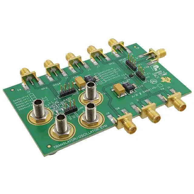
The translator/oscillator buffer evaluation module (EVM) allows evaluation of
the SN65LVDS16/17/18/19/20 and SN65LVP16/17/18/19/20 repeaters/translators/oscillators. This user’s guide provides a brief overview of the EVM, operation instructions, and output results.
Topic
Page
1.1
Evaluation Module U1 . . . . . . . . . . . . . . . . . . . . . . . . . . . . . . . . . . . . . . . . . 1-2
1.2
Applying an Input to EVM U1 . . . . . . . . . . . . . . . . . . . . . . . . . . . . . . . . . . . 1-2
1.3
Observing an EVM U1 Output . . . . . . . . . . . . . . . . . . . . . . . . . . . . . . . . . . 1-3
1.4
Evaluation Module U2 . . . . . . . . . . . . . . . . . . . . . . . . . . . . . . . . . . . . . . . . . 1-4
1.5
Applying an Input to EVM U2 . . . . . . . . . . . . . . . . . . . . . . . . . . . . . . . . . . . 1-4
1.6
Observing an EVM U2 Output . . . . . . . . . . . . . . . . . . . . . . . . . . . . . . . . . . 1-5
Introduction
1-1
�Evaluation Module U1
1.1 Evaluation Module U1
Figure 1−1. Power Connections for Evaluation Module U1
Power Supply 1
+
3.3V
−
Power Supply 2
+
1.2V
−
P4
DUT
GND
P3
EVM
GND
P2
VCC
J2
J1
R5
Uninstalled
EVM
50 Ω
50 Ω
Matched
Cables
SMA to SMA
J3
Oscilloscope
Warning
Power jacks P2, P3, and P4 are not insulated on the backside of the
EVM. Place the EVM on a nonconductive surface.
1.2 Applying an Input to EVM U1
For the oscillator gain stage/buffer the only requirement is to simply apply power to the EVM. The EVM has a crystal onboard that when powered up supplies
a signal to the SN65LVDS16, SN65LVP16, SN65LVDS18, or SN65LVP18
which provides a very clean 155.52 MHz signal at J1 and J2.
1-2
�Observing an EVM U1 Output
1.3 Observing an EVM U1 Output
The outputs are available at J1 and J2 for direct connection to oscilloscope inputs. Matched length cables must be used when connecting the EVM to a
scope to avoid inducing skew between the noninverting (+) and inverting (−)
outputs.
The three power jacks (P2, P3, and P4) are used to provide power and a
ground reference for the EVM. The power connections to the EVM determine
the common-mode load to the device. When connecting the EVM outputs directly to oscilloscope inputs, setting of the oscilloscope common-mode offset
voltage is required, as the oscilloscope presents low common-mode load impedance to the device.
Returning to Figure 1−1, Power Supply 1 is used to provide the required
3.3 V to the EVM. Power Supply 2 is used to offset the EVM ground relative
to the DUT ground. The EVM ground is connected to the oscilloscope ground
through the returns on SMA connectors J1 and J2. With power applied, the
common-mode voltage seen by the SN65LVDS16 or SN65LVDS18 is
approximately equal to the reference voltage being used inside the device
preventing significant common-mode current to flow. Optimum device setup
can be confirmed by adjusting the voltage on Power Supply 2 until its current
is minimized. It is important to note that use of the dual supplies, and offsetting
the EVM ground relative to the DUT ground are simply steps needed for test
and evaluation of devices. Actual designs would include high-impedance
receivers, which would not require the setup steps outlined above.
LVPECL drivers need a 50-Ω termination to VTT. A modification of Figure 1−1
and the above instructions are used when evaluating a SN65LVP16 or
SN65LVP18 with a direct connection to a 50-Ω oscilloscope. With Power
Supply 1 in Figure 1−1 set to 3.3 V, Power Supply 2 should be set to 1.3 V (2
V below VCC) to provide the correct termination voltage.
Note:
Power Supply 2 must be able to sink current.
Introduction
1-3
�Evaluation Module U2
1.4 Evaluation Module U2
Figure 1−2. Power Connections for Evaluation Module U2
Power Supply 1
+
3.3V
−
Power Supply 2
+
1.2V
−
P4
DUT
GND
P3
EVM
GND
P2
VCC
J5
J6
Pattern
Generator
Matched
Cables
SMA to SMA
J7
R6
100 Ω
R7
Uninstalled
EVM
J8
50 Ω
50 Ω
Matched
Cables
SMA to SMA
J9
Oscilloscope
Warning
Power jacks P2, P3, and P4 are not insulated on the backside of the
EVM. Place the EVM on a nonconductive surface.
1.5 Applying an Input to EVM U2
Inputs should be applied to SMA connectors J5 and J6, while keeping R6
installed. The EVM comes with a 100-Ω termination resistor (R6) installed
across the differential inputs for terminating the transmission line.
When using a general-purpose signal generator with 50-Ω output impedance,
make sure that the signal levels are between 0 V to VCC with respect to P4.
VID cannot exceed 2 V. A signal generator such as the Advantest D3186 can
simulate LVPECL, LVDS, or CML inputs.
LVPECL levels can be obtained with 100-Ω differential input termination by
setting the input generator to a common-mode of 0.7 V.
1-4
�Observing an EVM U2 Output
1.6 Observing an EVM U2 Output
The outputs are available at J8 and J7 for direct connection to oscilloscope inputs. Matched length cables must be used when connecting the EVM to a
scope to avoid inducing skew between the noninverting (+) and inverting (−)
outputs.
The three power jacks (P2, P3, and P4) are used to provide power and a
ground reference for the EVM. The power connections to the EVM determine
the common-mode load to the device. When connecting the EVM outputs directly to oscilloscope inputs, setting of the oscilloscope common-mode offset
voltage is required, as the oscilloscope presents low common-mode load impedance to the device.
Returning to Figure 1−2, Power Supply 1 is used to provide the required
3.3 V to the EVM. Power Supply 2 is used to offset the EVM ground relative
to the DUT ground. The EVM ground is connected to the oscilloscope ground
through the returns on SMA connectors J8 and J7. With power applied, the
common-mode voltage seen by the SN65LVDS20, SN65LVDS17, or
SN65LVDS19 is approximately equal to the reference voltage being used
inside the device preventing significant common-mode current to flow.
Optimum device setup can be confirmed by adjusting the voltage on Power
Supply 2 until its current is minimized. It is important to note that use of the dual
supplies, and offsetting the EVM ground relative to the DUT ground are simply
steps needed for test and evaluation of devices. Actual designs would include
high-impedance receivers, which would not require the setup steps outlined
above.
LVPECL drivers need a 50-Ω termination to VTT. A modification of Figure 1−1
and the above instructions are used when evaluating a SN65LVP20,
SN65LVP17, or SN65LVP19 with a direct connection to a 50-Ω oscilloscope.
With Power Supply 1 in Figure 1−2 set to 3.3 V, Power Supply 2 should be set
to 1.3 V (2 V below VCC) to provide the correct termination voltage.
Note:
Power Supply 2 must be able to sink current.
Introduction
1-5
�1-6
�Chapter 2
Bill of Materials and Schematic
This chapter contains the bill of materials and schematic.
Topic
Page
2.1
Bill of Materials . . . . . . . . . . . . . . . . . . . . . . . . . . . . . . . . . . . . . . . . . . . . . . . 2-2
2.2
Schematic . . . . . . . . . . . . . . . . . . . . . . . . . . . . . . . . . . . . . . . . . . . . . . . . . . . . 2-3
Bill of Materials and Schematic
2-1
�Bill of Materials
2.1 Bill of Materials
2-2
Item
Quantity
−1
Quantity
−2
1
1
−
C1
0.01 µF
ECJ−1VB1H103K
2
1
−
C2
27 pF
ECJ−OEC1H270J
3
1
−
C3
Uninstalled
Uninstalled
4
1
−
C4
0.001 µF
ECJ−OEB1H102K
5
1
−
C5
7 pF
ECJ−OEC1H070D
6
1
−
C6
15 pF
ECJ−OEC1H150J
7
1
−
C7
470 pF
ECJ−OEB1H471K
8
2
2
C8, C11
68 µF
592D686X0010R2T
9
2
2
C9, C12
10 µF
293D106X0035D2W
10
2
2
C10, C13
1 µF
12063G105ZATRA
11
−
1
C14
0.01 µF
ECJ−OEB1E103K
12
1
−
D1
SMV1253
SMV1253−079
Skyworks Solutions Inc.
13
1
1
JMP1, JMP3
3 Pin berg
(Make from AMP
4−103239−0)
14
1
1
JMP2, JMP4
4 Pin berg
(Make from AMP
4−103239−0)
15
3
5
J1, J2, J3, J4, J5,
J6, J7, J8, J9
SMA
142−0701−801
16
1
−
L1
180 nH
ELJ−RER18JF3
17
4
4
P1, P2, P3, P4
Banana−jack
3267
18
2
−
R1, R2
56.2 kΩ
ERJ−2RKF5622X
19
1
−
R3
2.21 kΩ
ERJ−2RKF2211X
20
1
−
R4
470 Ω
ERJ−2RKF4700X
21
1
1
R5, R7
49.9 Ω
ERJ−3EKF49R9V
(Uninstalled)
22
−
1
R6
100 Ω
ERJ−2RKF1000X
23
1
−
U1
LVP/16/18
SN65LVDS/P16/18
24
−
1
U2
LVDS/P
SN65LVDS/P/17/19/20
25
1
−
Y1
155.52 MHz
CWI45−B
Conner−Winfield Corp.
26
4
4
NA
Rubber feet
SJ5303−7−ND
27
1
1
NA
PWB
6464145
Reference
Value
Part No.
�Schematic
2.2 Schematic
The schematic for this device is attached.
Bill of Materials and Schematic
2-3
�5
4
3
2
1
VCC
VCC
P2
C1
100pf
D
C2
27pf
VCC01
1
C3
Uninstalled
C8
68uf
+
C4
C10
1uf
Banana-Jack
P3
1
L1
180 nH
R1
56.2K
C9
10uf
+
C11
68uf
+
.001uf
R3
2.2k
C12
10uf
+
C13
1uf
Banana-Jack
VCC01
P4
1
D1
SMV1253
VCC01
D
Banana-Jack
Y1
C
J2
C
LVDS/P/16/18
C5
1
2
3
4
C6
15pf
1
VCC01
P1
Banana-Jack
C7
470pf
VCC01
sma
8
7
6
5
R5
uninstalled
VCC
J1
sma
VCC
JMP2
3 pin berg
1
1
B
B
4
R4
470 ohm
R2
56.2K
U1
Q* VCC
D
Qhg
Vbb Qhg*
GC EN*
GND
9
3
7pf
2
155.52 Mhz
2
VCC01
VCC01
3
J3
JMP1
sma
A
A
Title
LVDS/P/16/17/18/19/20 EVM
Size
A
Date:
5
4
3
Document Number
6464145
Friday, August 27, 2004
2
Rev
A
Sheet
1
of
1
2
�5
4
3
2
1
D
D
J4
VCC
sma
C14
.01UF
J5
C
LVDS/P/17/19/20
sma
R6
100ohm
1
2
3
4
J6
U2
Q* VCC
D
Qhg
D* Qhg*
Vbb EN*
GND
9
J7
VCC01
C
sma
8
7
6
5
R7
uninstalled
J8
VCC01
sma
VCC
sma
JMP4
4
3
2
1
3 pin berg
1
VCC01
B
B
2
VCC01
3
J9
JMP3
sma
A
A
Title
LVDS/P/16/17/18/19/20 EVM
Size
A
Date:
5
4
3
Document Number
6464145
Friday, August 27, 2004
2
Rev
A
Sheet
2
of
1
2
�