SN65LVDS304
www.ti.com
SLLS764B – SEPTEMBER 2006 – REVISED FEBRUARY 2007
PROGRAMMABLE 27-BIT SERIAL-TO-PARALLEL RECEIVER
FEATURES
•
•
•
•
•
•
•
•
•
•
•
•
Serial Interface Technology
Compatible With FlatLink™3G Such as
SN65LVDS303
Supports Video Interfaces up to 24-Bit RGB
Data and 3 Control Bits Received Over 1 or 2
SubLVDS Differential Lines
SubLVDS Differential Voltage Levels
Up to 810-Mbps Data Throughput
Three Operating Modes to Conserve Power
– Active mode QVGA: 17 mW
– Typical Shutdown: 0.7 μW
– Typical Standby Mode: 27 μW Typical
Bus-Swap Function for PCB-Layout Flexibility
ESD Rating > 4 kV (HBM)
Pixel Clock Range of 4 MHz–30 MHz
Failsafe on all CMOS Inputs
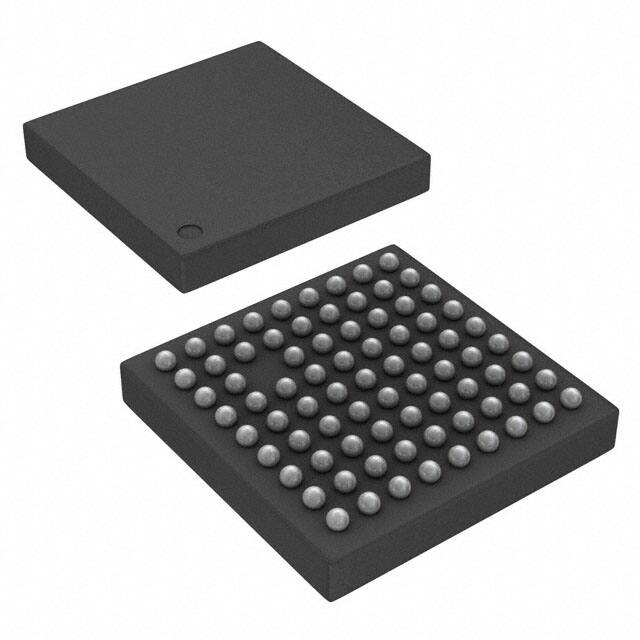
Packaged in 5-mm × 5-mm MicroStar Junior
μBGA® With 0,5-mm Ball Pitch
Very Low EMI Meets SAE J1752/3 'Kh'-Spec
APPLICATIONS
•
•
•
The serial data and clock are received via
sub-low-voltage differential signalling (SubLVDS)
lines. The SN65LVDS304 supports three operating
power modes (shutdown, standby, and active) to
conserve power.
When receiving, the PLL locks to the incoming clock
CLK and generates an internal high-speed clock at
the line rate of the data lines. The data is serially
loaded into a shift register using the internal
high-speed clock. The deserialized data is presented
on the parallel output bus with a recreation of the
pixel clock, PCLK, generated from the internal
high-speed clock. If no input CLK signal is present,
the output bus is held static with PCLK and DE held
low, while all other parallel outputs are pulled high.
The parallel (CMOS) output bus offers a bus-swap
feature. The SWAP control pin controls the output
pin order of the output pixel data to be either R[7:0].
G[7:0], B[7:0], VS, HS, DE or B[0:7], G[0:7], R[0:7],
VS, HS, DE. This gives a PCB designer the flexibility
to better match the bus to the LCD driver pinout or to
put the receiver device on the top side or the bottom
side of the PCB. The F/S control input selects
between a slow CMOS bus output rise time for best
EMI and power consumption and a fast CMOS
output for increased speed or higher-load designs.
Small Low-Emission Interface Between
Graphics Controller and LCD Display
Mobile Phones and Smart Phones
Portable Multimedia Players
DESCRIPTION
The
SN65LVDS304
receiver
deserializes
FlatLink™3G-compliant serial input data to 27
parallel data outputs. The SN65LVDS304 receiver
contains one shift register to load 30 bits from 1 or 2
serial inputs and latches the 24 pixel bits and 3
control bits out to the parallel CMOS outputs after
checking the parity bit. If the parity check confirms
correct parity, the channel parity error (CPE) output
remains low. If a parity error is detected, the CPE
output generates a high pulse while the data output
bus disregards the newly-received pixel. Instead, the
last data word is held on the output bus for another
clock cycle.
Flatlinkä3G
LCD
Driver
LVDS304
CLK
DATA
LVDS303
1
2
3
4
5
6
7
8
9
*
0
#
Application
Processor
with
RGB
Video
Interface
M0056-01
Please be aware that an important notice concerning availability, standard warranty, and use in critical applications of Texas
Instruments semiconductor products and disclaimers thereto appears at the end of this data sheet.
FlatLink is a trademark of Texas Instruments.
μBGA is a registered trademark of Tessera, Inc.
PRODUCTION DATA information is current as of publication date.
Products conform to specifications per the terms of the Texas
Instruments standard warranty. Production processing does not
necessarily include testing of all parameters.
Copyright © 2006–2007, Texas Instruments Incorporated
�SN65LVDS304
www.ti.com
SLLS764B – SEPTEMBER 2006 – REVISED FEBRUARY 2007
These devices have limited built-in ESD protection. The leads should be shorted together or the device placed in conductive foam
during storage or handling to prevent electrostatic damage to the MOS gates.
DESCRIPTION (CONTINUED)
The link select line, LS, selects whether 1 or 2 serial links are used. The RXEN input can be used to put the
SN65LVDS304 in a shutdown mode. The SN65LVDS304 enters an active standby mode if the common mode
voltage of the CLK input becomes shifted to VDDLVDS (e.g., transmitter releases CLK output into
high-impedance). This minimizes power consumption without the need of switching an external control pin. The
SN65LVDS304 is characterized for operation over ambient air temperatures of –40°C to 85°C. All CMOS and
SubLVDS signals are 2-V tolerant with VDD = 0 V. This feature allows signal powerup before VCC is stabilized.
FUNCTIONAL BLOCK DIAGRAM
VDDLVDS
RBBDC
CPE
iPCLK
D0+
50
Parity
Check
SubLVDS
50
SWAP
F/S
AND
D0–
8
1
50
SubLVDS
D1–
27-Bit Parallel
Register
D1+
50
R[0:7]
8
0
0
1
RGB = 1
HS = VS = 1
DE = 0
VDDLVDS
G[0:7]
Output Buffer
VDDLVDS
Serial-to-Parallel Conversion
RBBDC
8
B[0:7]
HS
VS
Standby or
Pwr Down
DE
RBBDC
CLK+
´15, or ´30
50
50
PLL
Multiplier
SubLVDS
CLK–
´1
iPCLK
0
PCLK
1
Standby
CPOL
Vthstby
RXEN
Glitch
Suppression
Control
LS
B0177-01
2
Submit Documentation Feedback
�SN65LVDS304
www.ti.com
SLLS764B – SEPTEMBER 2006 – REVISED FEBRUARY 2007
PINOUT – TOP VIEW
ZQE PACKAGE
(TOP VIEW)
4
5
6
7
8
9
R 4/B 3
R 2/B 5
R 0/B 7
G 6/G 1
G 4/G 3
G 2/G 5
GND
R 3/B 4
R 1/B 6
G 7/G 0
G 5/G 2
G 3/G 4
G 1/G 6
G 0/G 7
VDD
GND
VDD
GND
B 7/R 0
B 6/R 1
GND
GND
GND
GND
VDD
B 5 /R 2
B 4 /R 3
GNDPLLD
GND
GND
GND
GND
VDD
B 3/R 4
B 2/R 5
D1+
VDDPLLD
GND
GND
GND
GND
VDD
B 1/R 6
B 0/R 7
D1–
GNDLVDS
GND
GND
GND
GND
VDD
F/S
PCLK
CPOL
VDDLVDS
VDDPLLA
GNDPLLA
VDDLVDS
GNDLVDS
GND
VS
HS
GNDLVDS
SWAP
CLK+
CLK–
D0+
D0–
RXEN
DE
CPE
1
2
GND
R 6/B 1
R 7/B 0
R 5/B 2
LS
VDD
NC
GND
NC
3
A
B
C
D
E
F
G
H
J
RGB Output pin assignment based on SWAP pin setting:
SWAP = 0 / SWAP = 1
P0049-01
Submit Documentation Feedback
3
�SN65LVDS304
www.ti.com
SLLS764B – SEPTEMBER 2006 – REVISED FEBRUARY 2007
PINOUT – TOP VIEW (continued)
SWAP PIN FUNCTIONALITY
The SWAP pin allows the pcb designer to reverse the RGB bus, minimizing potential signal crossovers due to
signal routing. The two drawings beneath show the RGB signal pin assignment based on the SWAP-pin setting.
SN65LVDS304
(Top View)
SN65LVDS304
(Top View)
1
2
3
4
5
6
7
8
9
1
2
3
4
5
6
7
8
A
A
R6
R4
R2
R0
G6
G4
G2
R5
R3
R1
G7
G5
G3
G1
G0
B7
B6
B5
B4
B3
B2
B1
B0
B1
B3
B5
B7
G1
G3
G5
B2
B4
B6
G0
G2
G4
G6
G7
R0
R1
R2
R3
R4
R5
R6
R7
B
B
R7
B0
C
C
D
D
E
E
F
F
G
G
PCLK
PCLK
H
H
VS
VS
HS
HS
J
J
DE
DE
P0049-03
P0049-02
Figure 1. Pinout With SWAP PIN = GND
4
9
Submit Documentation Feedback
Figure 2. Pinout With SWAP PIN = VDD
�SN65LVDS304
www.ti.com
SLLS764B – SEPTEMBER 2006 – REVISED FEBRUARY 2007
PINOUT – TOP VIEW (continued)
Table 1. Pin Description
PIN
SWAP
SIGNAL
PIN
A1
–
GND
C1
L
R6
C2
H
B1
C3
A2
A3
A4
A5
A6
A7
A8
A9
B1
B2
B3
B4
B5
B6
B7
B8
B9
SWAP .
SIGNAL
PIN
SWAP
–
LS
F1
–
D1+
–
VDD
F2
–
VDDPLLD
F3
–
GND
unpopulated
SIGNAL
L
R4
C4
–
VDD
F4
–
GND
H
B3
C5
–
GND
F5
–
GND
L
R2
C6
–
VDD
F6
–
GND
H
B5
C7
–
GND
F7
–
VDD
L
R0
L
B7
H
B7
H
R0
L
G6
L
B6
H
G1
H
R1
H
R7
L
G4
D1
–
NC
G1
–
D1–
H
G3
D2
–
GND
G2
–
GNDLVDS
C8
C9
F8
F9
L
B1
H
R6
L
B0
L
G2
D3
–
GND
G3
–
GND
H
G5
D4
–
GND
G4
–
GND
–
GND
D5
–
GND
G5
–
GND
L
R7
D6
–
GND
G6
–
GND
H
B0
D7
–
VDD
G7
–
VDD
L
R5
L
B5
G8
–
F/S
H
B2
H
R2
G9
–
PCLK
L
R3
H
B4
L
R1
H
L
H
D8
L
B4
H1
–
CPOL
H
R3
H2
–
VDDLVDS
E1
–
NC
H3
–
VDDPLLA
B6
E2
–
GNDPLLD
H4
–
GNDPLLA
G7
E3
–
GND
H5
–
VDDLVDS
G0
E4
–
GND
H6
–
GNDLVDS
GND
D9
L
G5
E5
–
GND
H7
–
H
G2
E6
–
GND
H8
–
VS
L
G3
E7
–
VDD
H9
–
HS
H
G4
L
B3
J1
–
GNDLVDS
H
R4
J2
–
SWAP
L
B2
J3
–
CLK+
H
R5
J4
–
CLK–
J5
–
D0+
J6
–
D0–
J7
–
RXEN
J8
–
DE
J9
–
CPE
L
G1
H
G6
L
G0
H
G7
E8
E9
Submit Documentation Feedback
5
�SN65LVDS304
www.ti.com
SLLS764B – SEPTEMBER 2006 – REVISED FEBRUARY 2007
Table 2. TERMINAL FUNCTIONS
NAME
I/O
D0+, D0–
D1+, D1–
DESCRIPTION
SubLVDS data link (active during normal operation)
SubLVDS in
SubLVDS data link (active during normal operation when LS = high, high-impedance if LS = low); input
can be left open if unused.
CLK+, CLK–
SubLVDS input pixel clock; polarity is fixed.
R0–R7
Red-pixel data (8); pin assignment depends on SWAP pin setting.
G0–G7
Green-pixel data (8); pin assignment depends on SWAP pin setting.
B0–B7
Blue-pixel data (8); pin assignment depends on SWAP pin setting.
HS
CMOS out
Horizontal sync
VS
Vertical sync
DE
Data enable
PCLK
Output pixel clock; rising or falling clock polarity is selected by control input CPOL.
LS
Link select (determines active SubLVDS data links and PLL range); see Table 3.
Disables the CMOS Drivers and Turns Off the PLL, putting device in shutdown mode
1 – Receiver enabled
0 – Receiver disabled (shutdown)
Note: The RXEN input incorporates glitch suppression logic to avoid unwanted switching. The input
must be pulled low for longer than 10 μs continuously to force the receiver to enter shutdown. The input
must be pulled high for at least 10 μs continuously to activate the receiver. An input pulse shorter than
5 μs is interpreted as a glitch and becomes ignored. At power up, the receiver is enabled immediately if
RXEN = H and disabled if RXEN = L.
RXEN
CMOS In
CPOL
Output clock polarity selection
0 – rising edge clocking
1 – falling edge clocking
Bus swap swaps the bus pins to allow device placement on top or bottom of PCB. See pinout drawing
for pin assignments.
SWAP
0 – data output from R7...B0
1 – data output from B0...R7
CMOS bus rise time select
F/S
CPE
1 – fast-output rise time
0 – slow-output rise time
CMOS out
Channel parity error
This output indicates the detection of a parity error by generating an output high-pulse for half of a
PCLK clock cycle; this allows counting parity errors with a simple counter.
0 – no error
high-pulse – bit error detected
VDD
Supply voltage
GND
Supply ground
VDDLVDS
SubLVDS I/O supply voltage
GNDLVDS
VDDPLLA
6
Power supply
SubLVDS ground
PLL analog supply voltage
GNDPLLA
PLL analog GND
VDDPLLD
PLL digital supply voltage
GNDPLLD
PLL digital GND
Submit Documentation Feedback
�SN65LVDS304
www.ti.com
SLLS764B – SEPTEMBER 2006 – REVISED FEBRUARY 2007
FUNCTIONAL DESCRIPTION
Deserialization Modes
The SN65LVDS304 receiver has two modes of operation controlled by link-select pin LS. Table 3 shows the
deserializer modes of operation.
Table 3. Logic Table: Link Select Operating Modes
LS
MODE OF OPERATION
DATA LINKS STATUS
0
1ChM
1-channel mode (30-bit serialization rate)
D0 active
1
2ChM
2-channel mode (15-bit serialization rate)
D0, D1 active
1-Channel Mode
While LS is held low, the SN65LVDS304 receives payload data over a single SubLVDS data pair, D0. The PLL
locks to the SubLVDS clock input and internally multiplies the clock by a factor of 30. The internal high-speed
clock is used to shift in the data payload on D0 and to deserialize 30 bits of data. Figure 3 illustrates the timing
and the mapping of the data payload into the 30-bit frame. The internal high-speed clock is divided by a factor of
30 to recreate the pixel clock, and the data payload with the pixel clock is presented on the output bus. The
reserved bits and parity bit are not output. While in this mode, the PLL can lock to a clock that is in the range of
4 MHz through 15 MHz. This mode is intended for smaller video display formats that do not need the full
bandwidth capabilities of the SN65LVDS304.
CLK–
CLK+
D0+/– CHANNEL res res CP R7 R6 R5 R4 R3 R2 R1 R0 G7 G6 G5 G4 G3 G2 G1 G0 B7 B6 B5 B4 B3 B2 B1 B0 VS HS DE res res CP R7 R6
T0161-01
Figure 3. Data and Clock Input in 1-ChM (LS = low)
2-Channel Mode
While LS is held high, the SN65LVDS304 receives payload data over two SubLVDS data pairs, D0 and D1. The
PLL locks to the SubLVDS clock input and internally multiplies the clock by a factor of 15. The internal
high-speed clock is used to shift in the data payload on D0 and D1 and to deserialize 15 bits of data from each
pair. Figure 4 illustrates the timing and the mapping of the data payload into the 30-bit frame. The internal
high-speed clock is divided by a factor of 15 to recreate the pixel clock, and the data payload with pixel clock is
presented on the output bus. The reserved bits and parity bit are not output. While in this mode, the PLL can
lock to a clock that is in the range of 8 MHz through 30 MHz.
CLK–
CLK +
D0+/– Channel CP R7 R6 R5 R4 R3 R2 R1 R0 G7 G6 G5 G4 VS res CP R7 R6
D1+/– Channel res G3 G2 G1 G0 B7 B6 B5 B4 B3 B2 B1 B0 HS DE res G3 G2
T0162-01
Figure 4. Data and Clock Input in 2-ChM (LS = high)
POWER-DOWN MODES
The SN65LVDS304 receiver has two power-down modes to facilitate efficient power management.
SHUTDOWN MODE
A low input signal on the RXEN pin puts the SN65LVDS304 into shutdown mode. This turns off most of the
receiver circuitry including the SubLVDS receivers, PLL, and deserializers. The SubLVDS differential-input
resistance remains 100 Ω, and any input signal is ignored. All outputs hold a static output pattern:
R[0:7] = G[0:7] = B[0:7] = VS = HS = high; DE = PCLK = low.
Submit Documentation Feedback
7
�SN65LVDS304
www.ti.com
SLLS764B – SEPTEMBER 2006 – REVISED FEBRUARY 2007
The current draw in shutdown mode is nearly zero if the SubLVDS inputs are left open or pulled high.
STANDBY MODE
The SN65LVDS304 enters the standby mode when the SN65LVDS304 is not in shutdown mode but the
SubLVDS clock-input common-mode voltage is above 0.9 × VDDLVDS. The CLK input incorporates a pullup circuit
to shift the SubLVDS clock-input common-mode voltage to VDDLVDS in the absence of an input signal. All circuitry
except the SubLVDS clock-input standby monitor is shut down. The SN65LVDS304 also enters the standby
mode when the input clock frequency on the CLK input is less than 500 kHz. The SubLVDS input resistance
remains 100 Ω, and any input signal on the data inputs D0 and D1 is ignored. All outputs will hold a static output
pattern:
R[0:7] = G[0:7] = B[0:7] = VS = HS = high; DE = PCLK = low.
The current drawn in standby mode is very low.
ACTIVE MODES
A high input signal on RXEN combined with a CLK input signal switching faster than 3 MHz and VICM smaller
than 1.3 V forces the SN65LVDS304 into the active mode. Current consumption in the active mode depends on
operating frequency and the number of data transitions in the data payload. CLK-input frequencies between 3
MHz and 4 MHz activate the device, but proper PLL functionality is not assured. It is not recommended to
operate the SN65LVDS304 in active mode at CLK frequencies below 4 MHz.
ACQUIRE MODE (PLL Approaches Lock)
When the SN65LVDS304 is enabled and a SubLVDS clock input present, the PLL pursues lock to the input
clock. While the PLL pursues lock, the output data bus holds a static output pattern:
R[0:7] = G[0:7] = B[0:7] = VS = HS = high; DE = PCLK = low.
For proper device operation, the pixel clock frequency must fall within the valid fPCLK range specified under
recommended operating conditions. If the pixel clock frequency is larger than 3 MHz but smaller than fPCLK(min),
the SN65LVDS304 PLL is enabled. Under such conditions, it is possible for the PLL to lock temporarily to the
pixel clock, causing the PLL monitor to release the device into active receive mode. If this happens, the PLL
may or may not be properly locked to the pixel clock input, potentially causing data errors, frequency oscillation,
and PLL deadlock (loss of VCO oscillation).
RECEIVE MODE
After the PLL achieves lock the device enters the normal receive mode. The output data bus presents the
deserialized data. The PCLK output pin outputs the recovered pixel clock.
PARITY ERROR DETECTION AND HANDLING
The SN65LVDS304 receiver performs error checking on the basis of a parity bit that is transmitted across the
SubLVDS interface from the transmitting device. Once the SN65LVDS304 detects the presence of the clock and
the PLL has locked onto PCLK, then the parity is checked. Parity-error detection ensures detection of all
single-bit errors in one pixel and 50% of all multibit errors.
The parity bit covers the 27-bit data payload consisting of 24 bits of pixel data plus VS, HS, and DE. Odd-parity
bit signalling is used. The parity error is output on the CPE pin. If the sum of the 27 data bits and the parity bit
result in an odd number, the receive data are assumed to be valid. The CPE output is held low. If the sum
equals an even number, parity error is declared. The CPE output indicates high for half a PCLK period. The
CPE output is set with the data bit transition and cleared after 1/2 the data-bit time. This allows counting every
detected parity error with a simple counter connected to CPE.
If a parity error is detected, then the data on that PCLK cycle is not output. Instead, the last valid data from a
previous PCLK cycle is repeated on the output bus. This is to prevent any bit error that occurs on the LVDS link
from causing perturbations in VS, HS, or DE that might be visually disruptive to a display.
The reserved bits are not covered in the parity calculations.
8
Submit Documentation Feedback
�SN65LVDS304
www.ti.com
SLLS764B – SEPTEMBER 2006 – REVISED FEBRUARY 2007
A parity error is indicated by a
high pulse on CPE; the width of
the pulse is 1/2 the length of a
PCLK cycle.
CPE
R[0:7], G[0:7],
B[0:7], HS, VS, DE
PCLK
(CPOL = 0)
When a parity error is
detected, the receiver outputs
the previous pixel on the
bus. Hence, no data transitions
occur.
T0163-01
Figure 5. Parity Error Detection
STATUS-DETECT AND OPERATING-MODES FLOW DIAGRAM
The SN65LVDS304 switches between the power saving and active modes in the following way:
Power Up
RXEN = 1
CLK Input Inactive
RXEN Low
for > 10 ms
Power Up
RXEN = 0
Shutdown
Mode
Standby
Mode
RXEN High
for > 10 ms
VICM(CLK) > 0.9 VDDLVDS
RXEN Low
for > 10 ms
VICM(CLK) > 0.9 VDDLVDS
or fCLK < 500 kHz
CLK Input Active
Power Up
RXEN = 1
CLK Active
RXEN Low
for > 10 ms
Receive
Mode
PLL Achieved Lock
Acquire
Mode
F0017-01
Submit Documentation Feedback
9
�SN65LVDS304
www.ti.com
SLLS764B – SEPTEMBER 2006 – REVISED FEBRUARY 2007
Table 4. Status Detect and Operating Modes Descriptions
MODE
CHARACTERISTICS
CONDITIONS
RXEN is set low for longer than 10 μs.
(1) (2)
Shutdown mode
Least amount of power consumption (most circuitry turned
off); all outputs held static:
R[0:7] = G[0:7] = B[0:7] = VS = HS = high; DE = PCLK =
low
Standby mode
Low power consumption (standby monitor circuit active; PLL RXEN is high for longer than 10 μs and CLK inputs are
is shutdown to conserve power);
common-mode, VICM(CLK) is above 0.9 × VDDLVDS, or CLK
All outputs held static:
inputs are floating (2)
R[0:7] = G[0:7] = B[0:7] = VS = HS = high; DE = PCLK =
low
Acquire mode
PLL pursues lock; all outputs held static:
R[0:7] = G[0:7] = B[0:7] = VS = HS = high; DE = PCLK =
low
RXEN is high; CLK input monitor detected clock input
common mode and woke up receiver from standby
mode.
Receive mode
Data transfer (normal operation);
receiver deserializes data and provides data on parallel
output
RXEN is high and PLL is locked to incoming clock.
(1)
(2)
In shutdown mode, all SN65LVDS304 internal switching circuits (e.g., PLL, serializer, etc.) are turned off to minimize power
consumption. The input stage of any input pin remains active.
Leaving CMOS control inputs unconnected can cause random noise to toggle the input stage and potentially harm the device. All CMOS
inputs must be tied to a valid logic level, VIL or VIH, during shutdown or standby Mode. Exceptions are the SubLVDS inputs CLK and Dx,
which can be left unconnected while not in use.
Table 5. Operating Mode Transitions
MODE TRANSITION
USE CASE
Shutdown → standby
Drive RXEN high to enable
receiver.
TRANSITION SPECIFICS
1. RXEN high > 10 μs
2. Receiver enters standby mode.
a. R[0:7] = G[0:7] = B[0:7] = VS = HS remain high and DE = PCLK low
b. Receiver activates clock input monitor.
Standby → acquire
Transmitter activity
detected
1. CLK input monitor detects clock input activity.
2. Outputs remain static.
3. PLL circuit is enabled.
Acquire → receive
Link is ready to receive
data.
1. PLL is active and approaches lock.
2. PLL achieves lock within twakeup.
3. Input D0 or D1 becomes active, depending on LS selection.
4. First data word is recovered.
5. Parallel output bus turns on switching from a static output pattern to output the
first valid data word.
Receive → standby
Receive/standby →
shutdown
Transmitter requested to
enter standby mode by
input common mode
voltage VICM > 0.9 VDDLVDS
(e.g., transmitter output
clock stops or enters
high-impedance state)
1. Receiver disables outputs within tsleep.
Turn off receiver.
1. RXEN pulled low for > tpwrdn.
2. RX Input monitor detects VICM > 0.9 VDDLVDS within tsleep.
3. R[0:7] = G[0:7] = B[0:7] = VS = HS transition to high and DE = PCLK to low on
next falling PLL clock edge
4. PLL shuts down. Clock activity input monitor remains active.
2. R[0:7] = G[0:7] = B[0:7] = VS = HS remain static high or transition to static high
and DE = PCLK remain or transition to static low.
3. Most IC circuitry is shut down for least power consumption.
10
Submit Documentation Feedback
�SN65LVDS304
www.ti.com
SLLS764B – SEPTEMBER 2006 – REVISED FEBRUARY 2007
ABSOLUTE MAXIMUM RATINGS (1)
Supply voltage range, VDD
(2),
VDDPLLA, VDDPLLD, VDDLVDS
Voltage range at any input When VDDx > 0 V
or output terminal
When VDDx ≤ 0 V
V
±4
Charged-device model (4) (all pins)
±1500
Machine model (5) (all pins)
±200
V
kV
V
See Dissipation Ratings Table
±5
Ouput current, IO
(2)
(3)
(4)
(5)
–0.3 to 2.175
–0.5 to VDD + 2.175
Continuous power dissipation
(1)
UNIT
–0.5 to 2.175
Human body model (3) (all pins)
Electrostatic discharge
VALUE
mA
Stresses beyond those listed under absolute maximum ratings may cause permanent damage to the device. These are stress ratings
only and functional operation of the device at these or any other conditions beyond those indicated under recommended operating
conditions is not implied. Exposure to absolute maximum-rated conditions for extended periods may affect device reliability.
All voltage values are with respect to the GND terminals.
In accordance with JEDEC Standard 22, Test Method A114-B
In accordance with JEDEC Standard 22, Test Method C101
In accordance with JEDEC Standard 22, Test Method A115-A
DISSIPATION RATINGS
(1)
(2)
PACKAGE
CIRCUIT
BOARD MODEL
TA < 25°C
DERATING FACTOR (1)
ABOVE TA = 25°C
TA = 85°C
POWER RATING
ZQE
Low-K (2)
592 mW
7.407 mW/°C
148 mW
This is the inverse of the junction-to-ambient thermal resistance when board-mounted and with no air
flow.
In accordance with the low-K thermal metric definitions of EIA/JESD51-2.
DEVICE POWER DISSIPATION
PARAMETER
PD
Device power
dissipation
TEST CONDITIONS
VDDx = 1.8 V, TA = 25°C, all outputs terminated with 10 pF, fCLK at 4 MHz
VDDx = 1.95 V, TA = –40°C, all outputs terminated with 10 pF, fCLK at 30 MHz
Submit Documentation Feedback
TYP
MAX
16.8
72.2
UNIT
mW
11
�SN65LVDS304
www.ti.com
SLLS764B – SEPTEMBER 2006 – REVISED FEBRUARY 2007
RECOMMENDED OPERATING CONDITIONS (1)
VDD
VDDPLLA
VDDPLLD
VDDLVDS
Supply voltages
VDDn(PP)
Supply voltage noise magnitude
MIN
TYP
MAX
UNIT
1.65
1.8
1.95
V
Test set-up shown in Figure 7;
fCLK ≤ 50MHz; f(noise) = 1Hz to 2 GHz
100
mV
fCLK > 50MHz; f(noise) = 1Hz to 1MHz
100
fCLK > 50 MHz; f(noise) > 1MHz
TA
Operating free-air temperature
40
–40
85
1-channel transmit mode, see Figure 3
4
15
2-channel transmit mode, see Figure 4
8
30
°C
CLK+ and CLK–
fCLK±
Input pixel clock frequency
tDUTCLK
CLK input duty cycle
Standby mode (2), see Figure 16
MHz
500
kHz
35
65
%
70
200
mV
0.6
1.2
D0+, D0–, D1+, D1–, CLK+, and CLK–
|VID|
Magnitude of differential input voltage |VD0+ – VD0-|, |VD1+– VD1-|,
|VCLK+ – VCLK-| during normal operation
VICM
Input voltage common mode range
ΔVICM
Input voltage common mode variation VICM(n) – VICM(m) with n = D0, D1, or CLK
among all SubLVDS inputs
and m = D0, D1, or CLK
ΔVID
Differential input voltage amplitude
variation among all SubLVDS inputs
VID(n) – VID(m) with n = D0, D1, or CLK and
m = D0, D1, or CLK
tr/f
Input rise and fall times
RXEN at VDD; see Figure 10
Δtr/f
Input rise or fall time mismatch
among all SubLVDS inputs
tr(n) – tr(m) and tf(n) – tf(m) with n = D0, D1, or
CLK and m = D0, D1, or CLK
Receive or acquire mode
Standby mode
V
0.9
VDDLVDS
–100
100
mV
–10
10
%
800
ps
100
ps
V
–100
LS, CPOL, SWAP, RXEN, F/S
VICMOSH
High-level input voltage
0.7 VDD
VDD
VICMOSL
Low-level input voltage
0
0.3 VDD
tinRXEN
RXEN input pulse duration
V
μs
10
R[7:0], G[7:0], B[7:0], VS, HS, PCLK, CPE
CL
(1)
(2)
12
Output load capacitance
10
pF
Unused single-ended inputs must be held high or low to prevent them from floating.
PCLK input frequencies lower than 500 kHz force the SN65LVDS304 into standby mode. Input frequencies between 500 kHz and 3
MHz may or may not activate the SN65LVDS304. Input frequencies beyond 3 MHz activate the SN65LVDS304. Input frequencies
between 500 kHz and 4 MHz are not recommended, and can cause PLL malfunction.
Submit Documentation Feedback
�SN65LVDS304
www.ti.com
SLLS764B – SEPTEMBER 2006 – REVISED FEBRUARY 2007
DEVICE ELECTRICAL CHARACTERISTICS
over recommended operating conditions (unless otherwise noted)
PARAMETER
Alternating 1010 test pattern (see Table 9); all CMOS outputs
terminated with 10 pF; F/S and RXEN at VDD; VIH = VDD, VIL = 0 V; VDD
= VDDPLLA = VDDPLLD = VDDLVDS
1ChM
IDD
RMS supply
current
2ChM
Typical power test pattern (see Table 7); VID = 70 mV, all CMOS
outputs terminated with 10 pF; F/S at GND and RXEN at VDD; VIH =
VDD, VIL = 0 V; VDD = VDDPLLA = VDDPLLD = VDDLVDS
MAX
fPCLK = 4 MHz
9.8
14
fPCLK = 6 MHz
11.7
15.9
fPCLK = 15 MHz
19.3
25
fPCLK = 4 MHz
4.7
MIN
fPCLK = 6 MHz
6
13.2
Alternating 1010 test pattern (seeTable 9); all CMOS outputs
fPCLK = 8 MHz
terminated with 10 pF; F/S and RXEN at VDD; VIH = VDD, VIL = 0 V; VDD
fPCLK = 22 MHz
= VDDPLLA = VDDPLLD = VDDLVDS
fPCLK = 30 MHz
14.3
19.4
25
33
26.8
37
Typical power test pattern (see Table 8); VID = 70 mV, all CMOS
outputs terminated with 10 pF; F/S at GND and RXEN at VDD; VIH =
VDD, VIL = 0 V; VDD = VDDPLLA = VDDPLLD = VDDLVDS
UNIT
mA
mA
fPCLK = 15 MHz
CLK and D inputs are left open; all control inputs held static high or low;
All CMOS outputs terminated with 10 pF;
VIH = VDD, VIL = 0 V; VDD = VDDPLLA = VDDPLLD = VDDLVDS
(1)
TYP (1)
TEST CONDITIONS
fPCLK = 8 MHz
6.4
fPCLK = 22 MHz
13.7
fPCLK = 30 MHz
18.3
Standby mode;
RXEN = VIH
15
100
Shutdown
mode;
RXEN = VIL
0.4
10
mA
mA
μA
All typical values are at 25°C and with 1.8-V supply, unless otherwise noted.
Submit Documentation Feedback
13
�SN65LVDS304
www.ti.com
SLLS764B – SEPTEMBER 2006 – REVISED FEBRUARY 2007
INPUT ELECTRICAL CHARACTERISTICS
over operating free-air temperature range (unless otherwise noted)
PARAMETER
TEST CONDITIONS
MIN
TYP (1)
MAX
UNIT
D0+, D0–, D1+, D1–, CLK+, and CLK–
Vthstby
Input voltage common mode threshold to RXEN at VDD
switch between receive/acquire mode and
standby mode
VTHL
Low-level differential input voltage
threshold
VD0+– VD0–, VD1+– VD1,
VCLK+– VCLK-
VTHH
High-level differential input voltage
threshold
II+, II–
Input leakage current
VDD = 1.95 V; VI+ = VI–;
VI = 0.4 V and VI = 1.5 V
IIOFF
Power-off input current
VDD = GND; VI = 1.5 V
RID
Differential input termination resistor value
CIN
Input capacitance
Measured between input terminal
and GND
ΔCIN
Input capacitance variation
Within one signal pair
Between all signals
1.3
0.9 VDDLVDS
V
–40
mV
40
75
78
RBBDC Pullup resistor for standby detection
100
μA
–75
μA
122
Ω
1
21
mV
pF
30
0.2
1
pF
39
kΩ
LS, CPOL, SWAP, RXEN, F/S
VIK
Input clamp voltage
IICMOS Input current (2)
II = –18 mA, VDD = VDD(min)
–1.2
V
0 V ≤ VDD ≤ 1.95 V; VI = GND or VI
= 1.95 V
100
nA
CIN
Input capacitance
IIH
High-level input current
VIN = 0.7 VDD
–200
200
IIL
Low-level input current
VIN = 0.3 VDD
–200
200
VIH
High-level input voltage
0.7 VDD
VDD
VIL
Low-level input voltage
0
0.3 VDD
(1)
(2)
2
pF
nA
V
All typical values are at 25°C and with 1.8-V supply unless otherwise noted.
Do not leave any CMOS input unconnected or floating to minimize leakage currents. Every input must be connected to a valid logic
level, VIH or VOL, while power is supplied to VDD.
OUTPUT ELECTRICAL CHARACTERISTICS
over operating free-air temperature range (unless otherwise noted)
PARAMETER
TEST CONDITIONS
MIN
TYP
MAX
UNIT
0.8 VDD
VDD
V
0
0.2 VDD
V
R[0:7], G[0:7], B[0:7], VS, HS, PCLK, CPE
1-ChM, F/S = L, IOH = –250 μA
VOH
High-level output current
2-ChM, F/S = L, IOH = –500 μA
1-ChM, F/S = H, IOH = –500 μA
2-ChM, F/S = H, IOH = –2 mA
1-ChM, F/S = L, IOL = 250 μA
VOL
Low-level output current
IOH
High-level output current
2-ChM, F/S = L, IOL = 500 μA
1-ChM, F/S = H, IOL = 500 μA
2-ChM, F/S = H, IOL = 2 mA
1-ChM, F/S = L
2-ChM, F/S = L; 1-ChM, F/S = H
2-ChM, F/S = H
IOL
Low-level output current
1-ChM, F/S = L
2-ChM, F/S = L; 1-ChM, F/S = H
2-ChM, F/S = H
14
Submit Documentation Feedback
–250
–500
–2000
250
500
2000
μA
�SN65LVDS304
www.ti.com
SLLS764B – SEPTEMBER 2006 – REVISED FEBRUARY 2007
SWITCHING CHARACTERISTICS
over recommended operating conditions (unless otherwise noted)
PARAMETER
TEST CONDITIONS
MIN
TYP (1)
MAX
UNIT
800
ps
–100
100
ps
1-channel mode, F/S = L
8
16
2-channel mode, F/S = L
4
8
1-channel mode, F/S = H
4
8
D0+, D0–, D1+, D1–, CLK+, and CLK–
tr/f
Input rise and fall times
RXEN at VDD; see Figure 10
Δtr/f
Input rise or fall time
mismatch between all
SubLVDS inputs
tR(n) – tR(m) and tF(n) – tF(m) with n = D0, D1 or CLK
and m = D0, D1, or CLK
R[7:0], G[7:0], B[7:0], VS, HS, PCLK, CPE
Rise and fall time
20% ⇆ 80% of VDD (2)
tr/f
CL = 10 pF (3); see Figure 9
2-channel mode, F/S = H
tOUTP
PCLK output duty cycle
Output skew between PCLK
and R[0:7], G[0:7], B0:7],
HS, VS, and DE
tOSK
1
ns
2
1-channel mode
45%
50%
55%
CPOL = VIL, 2-channel mode
48%
53%
59%
CPOL = VIH, 2-channel mode
41%
47%
52%
See Figure 9.
–500
500
ps
2.5/fPCLK
s
3.8
μs
INPUT TO OUTPUT RESPONSE TIME
tPD(L)
Propagation delay time from
CLK+ input to PCLK output
RXEN at VDD, VIH = VDD, VIL = GND, CL = 10 pF, See
Figure 14
tGS
RXEN glitch suppression
pulse width (4)
VIH = VDD, VIL = GND, RXEN toggles between VIL and
VIH; see Figure 15 and Figure 16.
tpwrup
Enable time from power
down (↑RXEN)
Time from RXEN pulled high to data outputs enabled and
transmit valid data; see Figure 16.
2
ms
tpwrdn
Disable time from active
mode (↓RXEN)
RXEN is pulled low during receive mode; time
measurement until all outputs held static: R[0:7] = G[0:7]
= B[0:7] = VS = HS = high, DE = PCLK = low and PLL is
shut down; see Figure 16.
11
μs
twakeup
Enable time from standby
(↑↓CLK)
RXEN at VDD; device is in standby; time measurement
from CLK input starts switching to PCLK and data
outputs enabled and transmit valid data; see Figure 17.
2
ms
tsleep
Disable time from active
mode (CLK transitions to
high-impedance)
RXEN at VDD; device is receiving data; time
measurement from CLK input signal stops (input open or
input common mode VICM exceeds threshold voltage
Vthstby) until all outputs held static:
R[0:7] = G[0:7] = B[0:7] = VS = HS = high;
DE = PCLK = low and PLL is shut down;
see Figure 17.
3
μs
fBW
PLL bandwidth (5)
Tested from CLK input to PCLK output; 2-ChM; fPCLK =
22 MHz
(1)
(2)
(3)
(4)
(5)
1.4/fPCLK
0.087 fPCLK
1.9/fPCLK
MHz
All typical values are at 25°C and with 1.8-V supply, unless otherwise noted.
tR/F depends on the F/S setting and the capacitive load connected to each output. Some application information of how to calculate tR/F
based on the output load and how to estimate the timing budget to interconnect to an LCD driver are provided in the application section
near the end of this data sheet.
The output rise and fall times are optimized for an output load of 10 pF. The rise and fall times can be adjusted by changing the output
load capacitance.
The RXEN input incorporates glitch-suppression logic to disregard short input pulses. tGS is the duration of either a high-to-low or
low-to-high transition that is suppressed.
When using the SN65LVDS304 receiver in conjunction with the SN65LVDS303 transmitter in one link, the PLL bandwidth of the
SN65LVDS304 receiver always exceeds the bandwidth of the SN65LVDS303 transmit PLL. This ensures stable PLL tracking under all
operating conditions and maximizes the receiver skew margin.
Submit Documentation Feedback
15
�SN65LVDS304
www.ti.com
SLLS764B – SEPTEMBER 2006 – REVISED FEBRUARY 2007
12
10.0
11
10
9
4 MHz
9%
PLL – Bandwidth – %
PLL BW [% of PCLK Frequency]
9.5
RX PLL BW
9%
8.5%
8.2%
8
7.7%
7
6
8 MHz
9%
9.0
Spec Limit
1 ChM
8.5
Spec Limit
2 ChM
8.0
15 MHz
8.1 %
TX PLL BW
30 MHz
8.1 %
7.5
5
7.0
4
0
100
200
300
0
400
5
10
PLL Frequency − MHz
15
20
25
30
35
40
PCLK – Frequency – MHz
G001
Figure 6. SN65LVDS304 PLL Bandwidth (Also Showing the SN65LVDS303 PLL Bandwidth)
TIMING CHARACTERISTICS
PARAMETER
tRSKMx
(1) (2)
(1)
(2)
(3)
(4)
(5)
16
Receiver input skew
margin; see (3) and
Figure 36
TEST CONDITIONS
1ChM: x = 0..29, fPCLK = 15
MHz; RXEN at VDD, VIH = VDD,
VIL = GND, RL = 100 Ω, test
setup as in Figure 8, test pattern
as in Table 11
fCLK = 15 MHz (4)
2ChM: x = 0..14,
fPCLK =30 MHz
RXEN at VDD, VIH = VDD, VIL =
GND, RL = 100 Ω, test setup as
in Figure 8, test pattern as in
Table 12
fCLK = 30 MHz (4)
fCLK = 4 MHz to 15
MHz (5)
fCLK = 8 MHz to 30
MHz (5)
MIN
MAX
UNIT
630
1
- 480 ps
2 · 30 · fCLK
630
ps
1
- 480 ps
2 · 15 · fCLK
Receiver input skew margin (tRSKM) is the timing margin available for transmitter output pulse position (tPPOS), interconnect skew, and
interconnect inter-symbol interference. tRSKM represents the remainder of the serial bit time not taken up by the receiver strobe
uncertainty. tRSKM assumes a bit error rate better than 10–12.
tRSKM is inversely proportional to the internal setup and hold time uncertainty, ISI and duty cycle distortion from the front end receiver,
the skew missmatch between CLK and data D0 and D1, as well as the PLL cycle-to-cycle jitter.
This includes the receiver internal setup and hold time uncertainty, all PLL related high-frequency random and deterministic jitter
components that impact the jitter budget, ISI and duty cycle distortion from the front-end receiver, and the skew between CLK and data
D0 and D1; the pulse position minimum/maximum variation is given with a bit error rate target of 10–12; measurements of the total jitter
are taken over >10–12 samples.
The minimum and maximum limits are based on statistical analysis of the device performance over process, voltage, and temperature
ranges.
These minimum and maximum limits are simulated only.
Submit Documentation Feedback
�SN65LVDS304
www.ti.com
SLLS764B – SEPTEMBER 2006 – REVISED FEBRUARY 2007
PARAMETER MEASUREMENT INFORMATION
1
1
Noise
Generator
100 mV
VDDPLLA
2
SN65LVDS304
VDDPLLD
VDD
10 mF
VDDLVDS
GND
1.8-V
Supply
Note: The generator regulates the
noise amplitude at point 1 to the
target amplitude given under the table
Recommended Operating Conditions
S0216-01
Figure 7. Power-Supply Noise Test Setup
To measure tRSKM CLK is advanced or delayed with respect to data until errors are observed at the receiver outputs. The advance
or delay is then reduced until there are no data errors observed over 10
tRSKM
CLK and Data
Pattern
Generator
Programmable Delay
–12
serial bit times. The magnitude of the advance or delay
CLK
DUT:
SN65LVDS304
D0
Bit Error
Detector
D1
Ideal Receiver Strobe Position
tPG_ERROR
tRSKM(p)
C
tRSKM(n)
tbit
tRSKM
– is the smaller of the two measured values tRSKM(p) and tRSKM(n)
tPG_ERROR – Test equipment (pattern generator) intrinsic output pulse position timing uncertainty
tbit
– serial bit time
C
– LVDS304 set-up and hold-time uncertainty
Note: C can be derived by subtracting the receiver skew margin tRSKM(p) + tRSKM(p) from one serial bit time
T0164-01
Figure 8. Receiver Jitter-Budget Test Setup
Submit Documentation Feedback
17
�SN65LVDS304
www.ti.com
SLLS764B – SEPTEMBER 2006 – REVISED FEBRUARY 2007
PARAMETER MEASUREMENT INFORMATION (continued)
tF
t setup
80% (VOH -V OL )
R[7:0], G[7:0],
B[7:0], HS, VS, DE
20% (VOH -V OL )
t hold
t OSK
tR
VOH
80% (VOH -V OL )
PCLK
50% (VOH
- –VOL)
(CPOL=0)
20% (VOH -VOL )
VOL
tR
tF
Note:
The Set-up and Hold-time of CMOS outputs R[7:0], G[7:0],
B[7:0], HS, VS, and DE in relation to PCLK can be
calulated by:
1
tS&H =
2 -rPCLK -tREF - tOSK - DtDUTP
Figure 9. Output Rise/Fall, Setup/Hold Time
VDx+ – VDx– , VCLK+ – VCLK–
tf
80%(VID)
100%(VIC)
tr
0V
20%(VID)
0%(VID)
Figure 10. SubLVDS Differential Input Rise and Fall Time Defintion
CLK+, Dx+
VDDLVDS
RID/2
RBBDC
Gain
Stage
RID/2
CLK–, Dx–
Standby
Detection
Line End
Termination
ESD
S0224-02
Figure 11. Equivalent Input Circuit Design
18
Submit Documentation Feedback
�SN65LVDS304
www.ti.com
SLLS764B – SEPTEMBER 2006 – REVISED FEBRUARY 2007
PARAMETER MEASUREMENT INFORMATION (continued)
IICMOS
SWAP,
CPOL, LS,
RXEN, F/S
CMOS Input
(VI+ + VI–)/2
II+
VICMOS
CLK+, Dx+
VID
RGB, VS, HS,
CPE PCLK
IO
II–
CLK–, Dx–
VICM
VI+
VO
VI–
SubLVDS Input
CMOS Output
S0217-01
Figure 12. I/O Voltage and Current Definition
RGB, VS, HS,
CPE, PCLK
VO
SN65LVDS304
CL=10 pF
S0218-01
Figure 13. CMOS Output Test Circuit, Signal, and Timing Definition
Submit Documentation Feedback
19
�SN65LVDS304
www.ti.com
SLLS764B – SEPTEMBER 2006 – REVISED FEBRUARY 2007
PARAMETER MEASUREMENT INFORMATION (continued)
R7(n–2)
D0+
Pixel(n)
Pixel(n–1)
R7(n–1)
R7 R6 R5 R4
Pixel(n+1)
R7(n)
R7(n+1)
CP R7
CP R7
CLK–
CLK+
tPD(L)
VDD/2
PCLK
(CPOL = 0)
Pixel(n–1)
CMOS Data Out
R7
R7(n–3)
R7(n–1)
R6
R6(n–3)
R6(n–1)
Figure 14. Propagation Delay, Input to Output (LS = 0)
V DD /2
RXEN
t GS
CLK
t PLL
VCO Internal Signal
PLL Approaches Lock
t pwrup
PCLK
R[7:0], G[7:0], B[7:0], VS, HS
DE
Figure 15. Receiver Phase-Locked Loop Set TIme and Receiver Enable Time
20
Submit Documentation Feedback
�SN65LVDS304
www.ti.com
SLLS764B – SEPTEMBER 2006 – REVISED FEBRUARY 2007
PARAMETER MEASUREMENT INFORMATION (continued)
f (BWRX);
of total jitter above the receiver PLL bandwidth ; TJ TXPLL
TJ=RJ[ps-rms]*14 + DJ[ps]
t TXskew
: transmitter output skew (skew between CLK and data)
t TXIDJTransmitter Deterministic JItter of TX output stage (includes TX
Intersymbol Interference ISI)
RSPosn (max)
RSPosn (min)
SKEW
XTALK
RSPosn: Receiver input strobe position (min and max)
RSPosn(max) - RSPosn(min) = SkewRX + S&HRX + TJ (RXPLL(non-trackable)
PCB : PCB induced Skew (trace + connector);
: PCB induced cross-talk;
PCB
ISI PCB: Inter-symbol interference of PCB; is
dependent on interconnect frequency loss; may be
zero for short interconnects.
Skew RX: Receiver input skew (skew between CLK and Dx input)
S&H RX: Receiver input latch Sample & Hold uncertainty
TJ (RXPLL(non-trackable) : Intrinsic RX PLL jitter above RX PLL bandwidth; PLL
TJ >
f(BW RX ); TJ=RJ[ps-rms]*14 + DJ[ps]
T0165-01
Figure 36. Jitter Budget
Submit Documentation Feedback
33
�SN65LVDS304
www.ti.com
SLLS764B – SEPTEMBER 2006 – REVISED FEBRUARY 2007
F/S-PIN SETTING AND CONNECTING THE SN65LVDS304 TO AN LCD DRIVER
NOTE:
Receiver PLL tracking: To maximize the design margin for the interconnect, good
RX PLL tracking of the TX PLL is important. FlatLink3G requires the RX PLL to have
a bandwidth higher than the bandwidth of the TX PLL. The SN65LVDS304 PLL
design is optimized to track the SN65LVDS303 PLL particularly well, thus providing a
very large receiver skew margin. A FlatLink3G-compliant link must provide at least
±225 ppm of receiver skew margin for the interconnect.
It is important to understand the tradeoff between power consumption, EMI, and maximum speed when selecting
the F/S signal. It is beneficial to choose the slowest rise time possible to minimize EMI and power consumption.
Unfortunately a slower rise time also reduces the timing margin left for the LCD driver. Hence, it is necessary to
calculate the timing margin to select the correct F/S pin setting.
The output rise time depends on the output driver strength and the output load. An LCD driver typical capacitive
load is assumed with ~10 pF. The higher the capacitive load, the slower is the rise time. Rise time of the
SN65LVDS304 is measured as the time duration it takes the output voltage to rise from 20% of VDD to 80% of
VDD, and fall time is defined as the time for the output voltage to transition from 80% of VDD down to 20% of VDD.
Within one mode of operation and one F/S pin setting, the rise time of the output stage is fixed and does not
adjust to the pixel frequency. Due to the short bit time at very fast pixel clock speeds and the real capacitive load
of the display driver, the output amplitude might not reach VDD and GND saturation fully. To ensure sufficient
signal swing and verify the design margin, it becomes necessary to determine that the output amplitude under
any circumstance reaches the display driver’s input stage logic threshold (usually 30% and 70% of VDD).
Figure 37 shows a worst-case rise time simulation assuming an LCD driver load of 16 pF at VGA display
resolution. PCLK is the fastest-switching output. With F/S set to GND (Figure 37-a), the PCLK output voltage
amplitude is significantly reduced. The voltage amplitude of the output data RGB[7:0], VS, HS, and DE shows
less amplitude attenuation because these outputs carry random data patterns and toggle at half of the PCLK
frequency or less. It is necessary to determine the timing margin between the SN65LVDS304 output and LCD
driver input.
RX rise/fall time
Application: VGA (2-channel mode); F/S set to GND; Display driver load ~16 pF
RX rise/fall time
Application: VGA (2-channel mode); F/S set to VDD; Display driver load ~16 pF
2.0V
2.0V
1.8V
1.8V
1.6V
1.6V
1.4V
1.4V
1.2V
VOD
VOD
1.2V
(
1.0V
0.8V
0.6V
0.6V
0.4V
0.4V
0.2V
0.2V
0.0V
100ns
150ns
200ns
250ns
300ns
350ns
clk 22 MHz, F/S=1, CL=16 pF
400ns
450ns
500ns
550ns
600ns
The data signal has a slower maximum switching
frequency, and therefore drives a larger amplitude
than the clock signal
1.0V
0.8V
0.0V
100ns
150ns
200ns
250ns
300ns
350ns
clk 22 MHz, F/S=0, CL=16 pF
data 22 Mbps, F/S=1, CL=16 pF
400ns
450ns
500ns
data 22 Mbps, F/S=0, CL=16 pF
(b)
(a)
Figure 37. Output Amplitude as a Function of Output Toggling Frequency,
Capacitive Load, and F/S Setting
34
Submit Documentation Feedback
550ns
600ns
�SN65LVDS304
www.ti.com
SLLS764B – SEPTEMBER 2006 – REVISED FEBRUARY 2007
HOW TO DETERMINE THE LCD DRIVER TIMING MARGIN
To determine the timing margin, it is necessary to specify the frequency of operation, identify the setup and hold
times of the LCD driver, and specify the output load of the SN65LVDS304 as a combination of the LCD driver
input parasitics plus any capacitance caused by the connecting PCB trace. Furthermore, the setting of pin F/S
and the SN65LVDS304 output skew impact the margin. The total remaining design margin calculates as follows:
t rise(max) C LOAD
1
t DM +
* t DUTP(max_error) *
* Ťt OSKŤ
2 ƒ PCLK
10 pF
(3)
where:
tDM – Design margin
fPCLK – Pixel clock frequency
tDUTP(max_error) – maximum duty cycle error
trise(max) – maximum rise or fall time; see tR/F under switching characteristics
CL – parasitic capacitance (sum of LCD driver input parasitics + connecting PCB trace)
tskew – clock to data output skew SN65LVDS304
Example:
At a pixel clock frequeny of 5.5MHz (QVGA), and an assumed LCD driver load of 15 pF, the remaining timing
margin is:
Ť
Ť
t
(max) * 50
t DUTP(max_error) + DUTP
100%
t DM +
2
1
* 9ns *
5.5MHz
t PCLK + 5%
100%
16ns (FńS+GND)
10pF
1
+ 9.1ns
5.5MHz
15pF
* 500ps + 57.3ns
As long as the setup and hold times of the LCD driver are each less than 57 ns, the timing budget is met
sufficiently.
Submit Documentation Feedback
35
�PACKAGE OPTION ADDENDUM
www.ti.com
29-Aug-2015
PACKAGING INFORMATION
Orderable Device
Status
(1)
SN65LVDS304ZQER
ACTIVE
Package Type Package Pins Package
Drawing
Qty
BGA
MICROSTAR
JUNIOR
ZQE
80
Eco Plan
Lead/Ball Finish
MSL Peak Temp
(2)
(6)
(3)
TBD
Call TI
Call TI
Op Temp (°C)
Device Marking
(4/5)
-40 to 85
LVDS304
(1)
The marketing status values are defined as follows:
ACTIVE: Product device recommended for new designs.
LIFEBUY: TI has announced that the device will be discontinued, and a lifetime-buy period is in effect.
NRND: Not recommended for new designs. Device is in production to support existing customers, but TI does not recommend using this part in a new design.
PREVIEW: Device has been announced but is not in production. Samples may or may not be available.
OBSOLETE: TI has discontinued the production of the device.
(2)
Eco Plan - The planned eco-friendly classification: Pb-Free (RoHS), Pb-Free (RoHS Exempt), or Green (RoHS & no Sb/Br) - please check http://www.ti.com/productcontent for the latest availability
information and additional product content details.
TBD: The Pb-Free/Green conversion plan has not been defined.
Pb-Free (RoHS): TI's terms "Lead-Free" or "Pb-Free" mean semiconductor products that are compatible with the current RoHS requirements for all 6 substances, including the requirement that
lead not exceed 0.1% by weight in homogeneous materials. Where designed to be soldered at high temperatures, TI Pb-Free products are suitable for use in specified lead-free processes.
Pb-Free (RoHS Exempt): This component has a RoHS exemption for either 1) lead-based flip-chip solder bumps used between the die and package, or 2) lead-based die adhesive used between
the die and leadframe. The component is otherwise considered Pb-Free (RoHS compatible) as defined above.
Green (RoHS & no Sb/Br): TI defines "Green" to mean Pb-Free (RoHS compatible), and free of Bromine (Br) and Antimony (Sb) based flame retardants (Br or Sb do not exceed 0.1% by weight
in homogeneous material)
(3)
MSL, Peak Temp. - The Moisture Sensitivity Level rating according to the JEDEC industry standard classifications, and peak solder temperature.
(4)
There may be additional marking, which relates to the logo, the lot trace code information, or the environmental category on the device.
(5)
Multiple Device Markings will be inside parentheses. Only one Device Marking contained in parentheses and separated by a "~" will appear on a device. If a line is indented then it is a continuation
of the previous line and the two combined represent the entire Device Marking for that device.
(6)
Lead/Ball Finish - Orderable Devices may have multiple material finish options. Finish options are separated by a vertical ruled line. Lead/Ball Finish values may wrap to two lines if the finish
value exceeds the maximum column width.
Important Information and Disclaimer:The information provided on this page represents TI's knowledge and belief as of the date that it is provided. TI bases its knowledge and belief on information
provided by third parties, and makes no representation or warranty as to the accuracy of such information. Efforts are underway to better integrate information from third parties. TI has taken and
continues to take reasonable steps to provide representative and accurate information but may not have conducted destructive testing or chemical analysis on incoming materials and chemicals.
TI and TI suppliers consider certain information to be proprietary, and thus CAS numbers and other limited information may not be available for release.
Addendum-Page 1
Samples
�PACKAGE OPTION ADDENDUM
www.ti.com
29-Aug-2015
In no event shall TI's liability arising out of such information exceed the total purchase price of the TI part(s) at issue in this document sold by TI to Customer on an annual basis.
Addendum-Page 2
�PACKAGE MATERIALS INFORMATION
www.ti.com
16-Feb-2012
TAPE AND REEL INFORMATION
*All dimensions are nominal
Device
SN65LVDS304ZQER
Package Package Pins
Type Drawing
BGA MI
CROSTA
R JUNI
OR
ZQE
80
SPQ
Reel
Reel
A0
Diameter Width (mm)
(mm) W1 (mm)
2500
330.0
12.4
Pack Materials-Page 1
5.3
B0
(mm)
K0
(mm)
P1
(mm)
5.3
1.5
8.0
W
Pin1
(mm) Quadrant
12.0
Q1
�PACKAGE MATERIALS INFORMATION
www.ti.com
16-Feb-2012
*All dimensions are nominal
Device
Package Type
Package Drawing
Pins
SPQ
Length (mm)
Width (mm)
Height (mm)
SN65LVDS304ZQER
BGA MICROSTAR
JUNIOR
ZQE
80
2500
338.1
338.1
20.6
Pack Materials-Page 2
��IMPORTANT NOTICE
Texas Instruments Incorporated and its subsidiaries (TI) reserve the right to make corrections, enhancements, improvements and other
changes to its semiconductor products and services per JESD46, latest issue, and to discontinue any product or service per JESD48, latest
issue. Buyers should obtain the latest relevant information before placing orders and should verify that such information is current and
complete. All semiconductor products (also referred to herein as “components”) are sold subject to TI’s terms and conditions of sale
supplied at the time of order acknowledgment.
TI warrants performance of its components to the specifications applicable at the time of sale, in accordance with the warranty in TI’s terms
and conditions of sale of semiconductor products. Testing and other quality control techniques are used to the extent TI deems necessary
to support this warranty. Except where mandated by applicable law, testing of all parameters of each component is not necessarily
performed.
TI assumes no liability for applications assistance or the design of Buyers’ products. Buyers are responsible for their products and
applications using TI components. To minimize the risks associated with Buyers’ products and applications, Buyers should provide
adequate design and operating safeguards.
TI does not warrant or represent that any license, either express or implied, is granted under any patent right, copyright, mask work right, or
other intellectual property right relating to any combination, machine, or process in which TI components or services are used. Information
published by TI regarding third-party products or services does not constitute a license to use such products or services or a warranty or
endorsement thereof. Use of such information may require a license from a third party under the patents or other intellectual property of the
third party, or a license from TI under the patents or other intellectual property of TI.
Reproduction of significant portions of TI information in TI data books or data sheets is permissible only if reproduction is without alteration
and is accompanied by all associated warranties, conditions, limitations, and notices. TI is not responsible or liable for such altered
documentation. Information of third parties may be subject to additional restrictions.
Resale of TI components or services with statements different from or beyond the parameters stated by TI for that component or service
voids all express and any implied warranties for the associated TI component or service and is an unfair and deceptive business practice.
TI is not responsible or liable for any such statements.
Buyer acknowledges and agrees that it is solely responsible for compliance with all legal, regulatory and safety-related requirements
concerning its products, and any use of TI components in its applications, notwithstanding any applications-related information or support
that may be provided by TI. Buyer represents and agrees that it has all the necessary expertise to create and implement safeguards which
anticipate dangerous consequences of failures, monitor failures and their consequences, lessen the likelihood of failures that might cause
harm and take appropriate remedial actions. Buyer will fully indemnify TI and its representatives against any damages arising out of the use
of any TI components in safety-critical applications.
In some cases, TI components may be promoted specifically to facilitate safety-related applications. With such components, TI’s goal is to
help enable customers to design and create their own end-product solutions that meet applicable functional safety standards and
requirements. Nonetheless, such components are subject to these terms.
No TI components are authorized for use in FDA Class III (or similar life-critical medical equipment) unless authorized officers of the parties
have executed a special agreement specifically governing such use.
Only those TI components which TI has specifically designated as military grade or “enhanced plastic” are designed and intended for use in
military/aerospace applications or environments. Buyer acknowledges and agrees that any military or aerospace use of TI components
which have not been so designated is solely at the Buyer's risk, and that Buyer is solely responsible for compliance with all legal and
regulatory requirements in connection with such use.
TI has specifically designated certain components as meeting ISO/TS16949 requirements, mainly for automotive use. In any case of use of
non-designated products, TI will not be responsible for any failure to meet ISO/TS16949.
Products
Applications
Audio
www.ti.com/audio
Automotive and Transportation
www.ti.com/automotive
Amplifiers
amplifier.ti.com
Communications and Telecom
www.ti.com/communications
Data Converters
dataconverter.ti.com
Computers and Peripherals
www.ti.com/computers
DLP® Products
www.dlp.com
Consumer Electronics
www.ti.com/consumer-apps
DSP
dsp.ti.com
Energy and Lighting
www.ti.com/energy
Clocks and Timers
www.ti.com/clocks
Industrial
www.ti.com/industrial
Interface
interface.ti.com
Medical
www.ti.com/medical
Logic
logic.ti.com
Security
www.ti.com/security
Power Mgmt
power.ti.com
Space, Avionics and Defense
www.ti.com/space-avionics-defense
Microcontrollers
microcontroller.ti.com
Video and Imaging
www.ti.com/video
RFID
www.ti-rfid.com
OMAP Applications Processors
www.ti.com/omap
TI E2E Community
e2e.ti.com
Wireless Connectivity
www.ti.com/wirelessconnectivity
Mailing Address: Texas Instruments, Post Office Box 655303, Dallas, Texas 75265
Copyright © 2015, Texas Instruments Incorporated
�