Order
Now
Product
Folder
Technical
Documents
Support &
Community
Tools &
Software
SN65LVDT14, SN65LVDT41
SLLS530C – APRIL 2002 – REVISED FEBRUARY 2019
SN65LVDTxx multi-channel LVDS transceivers
SN65LVDT14—One LVDS driver plus four LVDS receivers
SN65LVDT41—Four LVDS drivers plus one LVDS receiver
1 Features
3 Description
•
The SN65LVDTxx devices are multi-channel LVDS
transceivers that operate using LVDS line drivers and
receivers. The SN65LVDTxx devices support
signaling rates of at least 250 Mbps, and the devices
operate from a single supply (typically at 3.3 V) in a
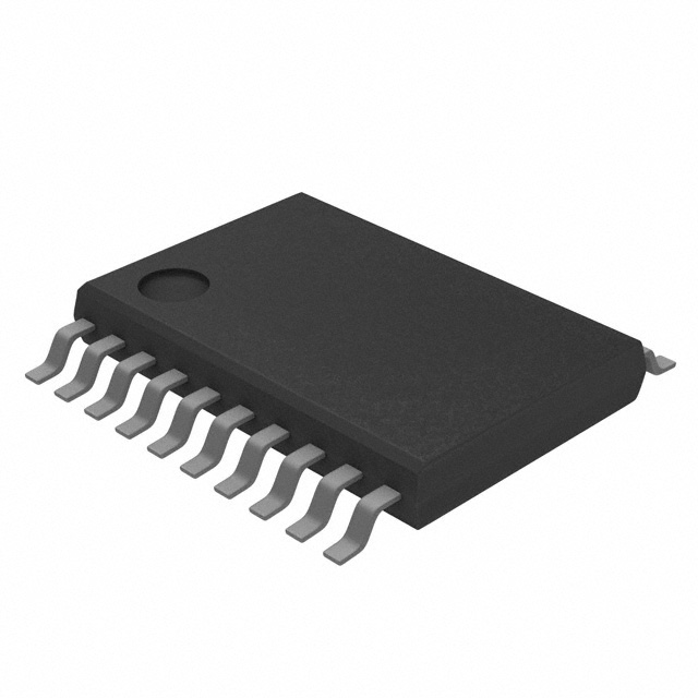
20-pin TSSOP package designed for easy PCB
layout.
1
•
•
•
•
•
•
•
Integrated 110-Ω nominal receiver line termination
resistor
Single 3.3-V power supply (3-V to 3.6-V range)
Supports signaling rates of at least 250 Mbps
Flow-through pinout simplifies PCB layout
LVTTL-compatible logic I/Os
ESD protection on bus pins exceeds 16 kV
Meets or exceeds the requirements of
ANSI/TIA/EIA-644A standard for LVDS
20-pin PW thin shrink small-outline package with
26-mil terminal pitch
2 Applications
•
•
•
•
•
•
•
•
Serial Peripheral Interface™ (SPI) over LVDS
allows long interconnects between master and
slave
Board-to-board communication
Test and measurement
Motor drives
LED video walls
Wireless infrastructure
Telecom infrastructure
Rack servers
The SN65LVDT14 and SN65LVDT41 provide
general-purpose,
asymmetric,
bidirectional
communication with the added benefit of high noise
immunity, low electromagnetic interference (EMI),
and increased cable length through the use of LVDS
lines. The SN65LVDT14 and SN65LVDT41 are
primarily used for SPI over LVDS applications.
The SN65LVDT14 combines one LVDS line driver
with four terminated LVDS line receivers in one
package. The SN65LVDT14 can be used to extend
asymmetric, bidirectional interfaces such as SPI over
long distances, and should be located at the SPI
slave.
The SN65LVDT41 combines four LVDS line drivers
with a single terminated LVDS line receiver in one
package. The SN65LVDT41 can be used to extend
asymmetric, bidirectional interfaces such as SPI over
long distances, and should be located at the SPI
master.
Device Information(1)
PART NUMBER
SN65LVDT14
SN65LVDT41
PACKAGE
BODY SIZE (NOM)
TSSOP (20)
6.50 mm × 4.40 mm
(1) For all available packages, see the orderable addendum at
the end of the data sheet.
SN65LVDT41 Functional Diagram
1D
2D
3D
4D
SN65LVDT14 Functional Diagram
1Y
1A
1Z
1B
1R
2Y
2A
2Z
3Y
2B
3Z
3B
4Y
4A
4Z
4B
5A
5Y
5B
5Z
3A
2R
3R
4R
5D
5R
1
An IMPORTANT NOTICE at the end of this data sheet addresses availability, warranty, changes, use in safety-critical applications,
intellectual property matters and other important disclaimers. PRODUCTION DATA.
�SN65LVDT14, SN65LVDT41
SLLS530C – APRIL 2002 – REVISED FEBRUARY 2019
www.ti.com
Table of Contents
1
2
3
4
5
6
7
8
Features ..................................................................
Applications ...........................................................
Description .............................................................
Revision History.....................................................
Pin Configuration and Functions .........................
Specifications.........................................................
1
1
1
2
3
5
6.1
6.2
6.3
6.4
6.5
6.6
6.7
6.8
6.9
6.10
5
5
5
6
6
7
7
7
7
8
Absolute Maximum Ratings ......................................
ESD Ratings..............................................................
Recommended Operating Conditions.......................
Thermal Information ..................................................
Receiver Electrical Characteristics ...........................
Driver Electrical Characteristics ................................
Device Electrical Characteristics...............................
Receiver Switching Characteristics...........................
Driver Switching Characteristics ...............................
Typical Characteristics ............................................
Parameter Measurement Information .................. 9
Detailed Description ............................................ 12
8.1 Overview ................................................................. 12
8.2 Functional Block Diagram ....................................... 12
8.3 Feature Description................................................. 12
8.4 Device Functional Modes........................................ 14
9
Application and Implementation ........................ 15
9.1 Application Information............................................ 15
9.2 Typical Application ................................................. 16
10 Power Supply Recommendations ..................... 20
11 Layout................................................................... 20
11.1 Layout Guidelines ................................................. 20
11.2 Layout Examples ................................................. 24
12 Device and Documentation Support ................. 26
12.1
12.2
12.3
12.4
12.5
12.6
12.7
Related Documentation .......................................
Receiving Notification of Documentation Updates
Related Links ........................................................
Community Resources..........................................
Trademarks ...........................................................
Electrostatic Discharge Caution ............................
Glossary ................................................................
26
26
26
26
26
26
27
13 Mechanical, Packaging, and Orderable
Information ........................................................... 27
4 Revision History
NOTE: Page numbers for previous revisions may differ from page numbers in the current version.
Changes from Revision B (Feburary 2006) to Revision C
Page
•
Added Device Information table, ESD Ratings table, Feature Description section, Device Functional Modes,
Application and Implementation section, Power Supply Recommendations section, Layout section, Device and
Documentation Support section, and Mechanical, Packaging, and Orderable Information section....................................... 1
•
Added navigation links and removed the NRND banner from the top of the datasheet page .............................................. 1
•
Moved power dissipation parameter to the Absolute Maximum Ratings table....................................................................... 5
2
Submit Documentation Feedback
Copyright © 2002–2019, Texas Instruments Incorporated
Product Folder Links: SN65LVDT14 SN65LVDT41
�SN65LVDT14, SN65LVDT41
www.ti.com
SLLS530C – APRIL 2002 – REVISED FEBRUARY 2019
5 Pin Configuration and Functions
SN65LVDT41 PW Package
20-Pin TSSOP
Top View
1D
GND
2D
VCC
3D
GND
4D
VCC
5R
GND
1
2
3
4
5
6
7
8
9
10
20
19
18
17
16
15
14
13
12
11
1Y
1Z
2Y
2Z
3Y
3Z
4Y
4Z
5A
5B
*marked as LVDT41
SN65LVDT41 Pin Functions
PIN
NAME
NO.
1D (1)
1
2D (1)
3
(1)
5
3D
4D (1)
7
1Y (1)
20
2Y (1)
18
(1)
16
4Y (1)
14
1Z (1)
19
(1)
17
3Z (1)
15
4Z (1)
13
3Y
2Z
I/O
DESCRIPTION
I
LVTTL Driver Input Pin
O
Noninverting LVDS Driver Output Pin
O
Inverting LVDS Driver Output Pin
5R
9
O
LVTTL Receiver Output Pin
5A
12
I
Noninverting LVDS Receiver Input Pin
5B
11
I
Inverting LVDS Receiver Input Pin
VCC
4, 8
I
Power Supply Pin, +3.3 V ± 0.3 V
GND
2, 6, 10
I
Ground Pin
(1)
x = 1, 2, 3, 4 indicating channel number of SN65LVDT41
Copyright © 2002–2019, Texas Instruments Incorporated
Product Folder Links: SN65LVDT14 SN65LVDT41
Submit Documentation Feedback
3
�SN65LVDT14, SN65LVDT41
SLLS530C – APRIL 2002 – REVISED FEBRUARY 2019
www.ti.com
SN65LVDT14 PW Package
20-Pin TSSOP
Top View
1A
1B
2A
2B
3A
3B
4A
4B
5Y
5Z
1
2
3
4
5
6
7
8
9
10
20
19
18
17
16
15
14
13
12
11
1R
GND
2R
VCC
3R
GND
4R
VCC
5D
GND
*marked as LVDT14
SN65LVDT14 Pin Functions
PIN
NAME
NO.
1A (1)
1
2A (1)
3
(1)
5
4A (1)
7
1B (1)
2
2B (1)
4
(1)
6
3A
3B
4B (1)
8
1R (1)
20
2R (1)
18
3R (1)
16
4R (1)
14
I/O
DESCRIPTION
I
Noninverting LVDS Receiver Input Pin
I
Inverting LVDS Receiver Input Pin
O
LVTTL Receiver Output Pin
5Y
9
I
Noninverting LVDS Driver Output Pin
5Z
10
I
Inverting LVDS Driver Output Pin
5D
12
O
LVTTL Driver Input Pin
GND
11, 15, 19
I
Ground Pin
VCC
13, 17
I
Power Supply Pin, +3.3 V ± 0.3 V
(1)
4
x = 1, 2, 3, 4 indicating channel number of SN65LVDT41
Submit Documentation Feedback
Copyright © 2002–2019, Texas Instruments Incorporated
Product Folder Links: SN65LVDT14 SN65LVDT41
�SN65LVDT14, SN65LVDT41
www.ti.com
SLLS530C – APRIL 2002 – REVISED FEBRUARY 2019
6 Specifications
6.1 Absolute Maximum Ratings
over operating free-air temperature range unless otherwise noted (1)
Supply voltage (2)
Input voltage
MIN
MAX
UNIT
VCC
–0.5
4
V
D or R
–0.5
6
V
A, B, Y, or Z
–0.5
4
V
260
°C
Lead temperature 1,6 mm (1/16 inch) from case for 10 seconds
Continuous total power
dissipation
TA < 25°C power rating
774
TA = 85°C power rating
402
Operating factor above TA = 25°C
6.2
mW/°C
150
°C
Storage temperature, Tstg
(1)
(2)
–65
mW
Stresses beyond those listed under absolute maximum ratings may cause permanent damage to the device. These are stress ratings
only, and functional operation of the device at these or any other conditions beyond those indicated under recommended operating
conditions is not implied. Exposure to absolute-maximum-rated conditions for extended periods may affect device reliability.
All voltage values, except differential I/O bus voltages are with respect to network ground terminal.
6.2 ESD Ratings
VALUE
V(ESD)
Electrostatic discharge
Human-body model (HBM), per
ANSI/ESDA/JEDEC JS-001 (1)
All pins except A, B, Y, Z,
and GND (2)
±8000
Pins A, B, Y, Z, and
GND (3)
±16000
Charged-device model (CDM), per JEDEC specification JESD22-C101 (4) (5)
(1)
(2)
(3)
(4)
(5)
UNIT
V
±500
Tested in accordance with JEDEC Standard 22, Test Method A114-A.
JEDEC document JEP155 states that 500-V HBM allows safe manufacturing with a standard ESD control process. Pins listed as ±8000
V may actually have higher performance.
JEDEC document JEP155 states that 500-V HBM allows safe manufacturing with a standard ESD control process. Pins listed as
±16000 V may actually have higher performance.
JEDEC document JEP157 states that 250-V CDM allows safe manufacturing with a standard ESD control process. Pins listed as ±500 V
may actually have higher performance.
Tested in accordance with JEDEC Standard 22, Test Method C101.
6.3 Recommended Operating Conditions
MIN
NOM
MAX
VCC
Supply voltage
3
3.3
3.6
VIH
High-level input voltage
2
VIL
Low-level input voltage
|VID|
Magnitude of differential input voltage
VIC
Common-mode input voltage, See Figure 1
TA
Operating free-air temperature
ŤV Ť
Copyright © 2002–2019, Texas Instruments Incorporated
Product Folder Links: SN65LVDT14 SN65LVDT41
0.8
V
0.6
V
ŤV Ť
2.4 *
–40
V
V
0.1
ID
2
UNIT
ID
2
V
VCC – 0.8
V
85
°C
Submit Documentation Feedback
5
�SN65LVDT14, SN65LVDT41
SLLS530C – APRIL 2002 – REVISED FEBRUARY 2019
www.ti.com
2.5
VIC − Common-Mode Input Voltage − V
Max at VCC > 3.15 V
Max at VCC = 3 V
2
1.5
1
0.5
Minimum
0
0
0.1
0.2
0.3
0.4
0.5
0.6
|VID|− Differential Input Voltage − V
Figure 1. VIC vs VID and VCC
6.4 Thermal Information
SN65LVDTxx
THERMAL METRIC (1)
PW (TSSOP)
UNIT
20 PINS
RθJA
Junction-to-ambient thermal resistance
86.9
°C/W
RθJC(top)
Junction-to-case (top) thermal resistance
28.4
°C/W
RθJB
Junction-to-board thermal resistance
38.2
°C/W
ψJT
Junction-to-top characterization parameter
1.4
°C/W
ψJB
Junction-to-board characterization parameter
37.8
°C/W
(1)
For more information about traditional and new thermal metrics, see the Semiconductor and IC Package Thermal Metrics application
report (SPRA953).
6.5 Receiver Electrical Characteristics
over operating free-air temperature range unless otherwise noted
PARAMETER
TEST CONDITIONS
MIN
TYP (1)
MAX
Positive-going differential input voltage threshold
VITH-
Negative-going differential input voltage threshold
VOH
High-level output voltage
IOH = -8 mA
VOL
Low-level output voltage
IOL = 8 mA
0.4
V
II
Input current (A or B inputs)
VI = 0 V and VI = 2.4 V,
other input open
±40
µA
II(OFF)
Power-off input current (A or B inputs)
VCC = 0 V, VI = 2.4 V
±40
µA
Ci
Input capacitance, A or B input to GND
VI = A sin 2πft + CV
Zt
Termination impedance
VID = 0.4 sin2.5E09 t V
(1)
6
See Figure 8 and Table 1
100
UNIT
VITH+
–100
2.4
V
5
88
mV
pF
132
Ω
All typical values are at 25°C and with a 3.3-V supply.
Submit Documentation Feedback
Copyright © 2002–2019, Texas Instruments Incorporated
Product Folder Links: SN65LVDT14 SN65LVDT41
�SN65LVDT14, SN65LVDT41
www.ti.com
SLLS530C – APRIL 2002 – REVISED FEBRUARY 2019
6.6 Driver Electrical Characteristics
over operating free-air temperature range unless otherwise noted
PARAMETER
TEST CONDITIONS
|VOD|
Differential output voltage magnitude
Δ|VOD|
Change in differential output voltage magnitude between
logic states
VOC(SS)
Steady-state common-mode output voltage
ΔVOC(SS)
Change in steady-state common-mode output voltage
between logic states
VOC(PP)
Peak-to-peak common-mode output voltage
IIH
High-level input current
IIL
Low-level input current
IOS
Short-circuit output current
IO(OFF)
Power-off output current
(1)
RL = 100 Ω,
See Figure 9 and
Figure 12
MIN
TYP (1)
MAX
247
340
454
UNIT
mV
–50
50
1.125
1.375
–50
50
mV
150
mV
VIH = 2 V
20
µA
VIL = 0.8 V
10
µA
See Figure 13
50
VOY or VOZ = 0 V
±24
VOD = 0 V
±12
VCC = 1.5 V, VO = 2.4 V
±1
V
mA
µA
All typical values are at 25°C and with a 3.3-V supply.
6.7 Device Electrical Characteristics
over operating free-air temperature range unless otherwise noted
PARAMETER
ICC
(1)
Supply current
TEST CONDITIONS
SN65LVDT14
SN65LVDT41
TYP (1)
MIN
MAX
25
Driver RL = 100 Ω, Driver VI = 0.8 V or 2 V,
Receiver VI = ±0.4 V
35
UNIT
mA
All typical values are at 25°C and with a 3.3-V supply.
6.8 Receiver Switching Characteristics
over operating free-air temperature range unless otherwise noted
PARAMETER
TEST CONDITIONS
tPLH
Propagation delay time, low-to-high-level output
tPHL
Propagation delay time, high-to-low-level output
tr
Output signal rise time
tf
Output signal fall time
tsk(p)
Pulse skew (|tPHL - tPLH|)
Output skew
tsk(pp)
Part-to-part skew (2)
(2)
NOM
MAX
1
2.6
3.8
ns
UNIT
1
2.6
3.8
ns
0.15
1.2
ns
0.15
1.2
ns
150
600
ps
100
400
ps
1
ns
(1)
tsk(o)
(1)
CL = 10 pF, See Figure 11
MIN
tsk(o) is the magnitude of the time difference between the tpLH or tpHL of all the receivers of a single device with all of their inputs
connected together.
tsk(pp) is the magnitude of the difference in propagation delay times between any specified terminals of two devices when both devices
operate with the same supply voltages, at the same temperature, and have identical packages and test circuits.
6.9 Driver Switching Characteristics
over operating free-air temperature range unless otherwise noted
PARAMETER
TEST CONDITIONS
tPLH
Propagation delay time, low-to-high-level output
tPHL
Propagation delay time, high-to-low-level output
tr
Differential output signal rise time
tf
Differential output signal fall time
RL = 100 Ω, CL = 10 pF,
See Figure 14
Copyright © 2002–2019, Texas Instruments Incorporated
Product Folder Links: SN65LVDT14 SN65LVDT41
MIN
NOM
MAX
0.9
1.7
2.9
0.9
1.6
2.9
0.26
1
0.26
1
Submit Documentation Feedback
UNIT
ns
7
�SN65LVDT14, SN65LVDT41
SLLS530C – APRIL 2002 – REVISED FEBRUARY 2019
www.ti.com
Driver Switching Characteristics (continued)
over operating free-air temperature range unless otherwise noted
PARAMETER
tsk(p)
Pulse skew (|tPHL - tPLH|)
tsk(o)
Output skew (1)
tsk(pp)
Part-to-part skew (2)
(1)
(2)
TEST CONDITIONS
MIN
NOM
MAX
UNIT
150
500
ps
80
150
ps
1.5
ns
RL = 100 Ω, CL = 10 pF,
See Figure 14
tsk(p) is the magnitude of the time difference between the high-to-low and low-to-high propagation delay times at an output.
tsk(pp) is the magnitude of the difference in propagation delay times between any specified terminals of two devices when both devices
operate with the same supply voltages, at the same temperature, and have identical packages and test circuits.
6.10 Typical Characteristics
6.10.1 Receiver
5
4
3
2.5
2
1.5
1
0.5
0
−70
TA = 25°C,
VCC = 3.3 V
4.5
VOL − Low-Level Output Voltage − V
VOH − High-Level Output Voltage − V
3.5
TA = 25°C,
VCC = 3.3 V
4
3.5
3
2.5
2
1.5
1
0.5
0
−60
−50
−40
−30
−20
−10
0
0
3
2.9
VCC = 3 V
2.8
VCC = 3.3 V
2.7
2.6
VCC = 3.6 V
2.4
2.3
2.2
−50
−25
0
25
50
75
TA − Free-Air Temperature − °C
100
Figure 4. Low-to-High Propagation Delay Time Vs Free-Air
Temperature
8
Submit Documentation Feedback
20
30
40
50
60
70
80
Figure 3. Low-Level Output Voltage vs Low-Level Output
Current
t PHL − High-To-Low Propagation Delay Time − ns
t PLH − Low-To-High Propagation Delay Time − ns
Figure 2. High-Level Output Voltage vs High-Level Output
Current
2.5
10
IOL − Low-Level Output Current − mA
IOH − High-Level Output Current − mA
2.8
2.7
2.6
VCC = 3 V
2.5
VCC = 3.3 V
2.4
VCC = 3.6 V
2.3
2.2
2.1
2
−50
−25
0
25
50
75
100
TA − Free-Air Temperature − °C
Figure 5. High-to-Low Propagation Delay Time vs Free-Air
Temperature
Copyright © 2002–2019, Texas Instruments Incorporated
Product Folder Links: SN65LVDT14 SN65LVDT41
�SN65LVDT14, SN65LVDT41
www.ti.com
SLLS530C – APRIL 2002 – REVISED FEBRUARY 2019
2.1
2
t PHL − High-To-Low Propagation Delay Time − ns
t PLH − Low-To-High Propagation Delay Time − ns
6.10.2 Driver
VCC = 3 V
1.9
1.8
VCC = 3.6 V
1.7
1.6
VCC = 3.3 V
1.5
−50
2.2
2.1
VCC = 3 V
2
VCC = 3.3 V
1.9
1.8
1.7
VCC = 3.6 V
1.6
1.5
−50
TA − Free-Air Temperature − °C
−25
0
25
50
75
Ta − Free-Air Temperature − °C
Figure 6. Low-to-High Propagation Delay Time vs Free-Air
Temperature
Figure 7. High-to-Low Propagation Delay Time vs Free-Air
Temperature
−25
0
25
50
75
100
100
7 Parameter Measurement Information
A
V
IA
)V
IB
VID
2
R
VIA
B
VIC
VO
VIB
Figure 8. Receiver Voltage Definitions
Table 1. Receiver Minimum and Maximum Input Threshold Test Voltages
APPLIED VOLTAGES
RESULTING DIFFERENTIAL
INPUT VOLTAGE
RESULTING
COMMON-MODE
INPUT VOLTAGE
VIA
VIB
VID
VIC
1.25 V
1.15 V
100 mV
1.2 V
1.15 V
1.25 V
–100 mV
1.2 V
2.4 V
2.3 V
100 mV
2.35 V
2.3 V
2.4 V
–100 mV
2.35 V
0.1 V
0.0 V
100 mV
0.05 V
0.0 V
0.1 V
–100 mV
0.05 V
1.5 V
0.9 V
600 mV
1.2 V
0.9 V
1.5 V
–600 mV
1.2 V
2.4 V
1.8 V
600 mV
2.1 V
1.8 V
2.4 V
–600 mV
2.1 V
0.6 V
0.0 V
600 mV
0.3 V
0.0 V
0.6 V
–600 mV
0.3 V
Copyright © 2002–2019, Texas Instruments Incorporated
Product Folder Links: SN65LVDT14 SN65LVDT41
Submit Documentation Feedback
9
�SN65LVDT14, SN65LVDT41
SLLS530C – APRIL 2002 – REVISED FEBRUARY 2019
www.ti.com
IOY
Y
II
D
IOZ
VOD
V
VOY
Z
VI
OY
)V
OZ
2
VOC
VOZ
Figure 9. Driver Voltage and Current Definitions
VID
VIA
VIB
CL
10 pF
VO
Figure 10. Receiver Timing Test Circuit
VIA
1.4 V
VIB
1V
VID
0.4 V
0V
–0.4 V
tPHL
VO
tPLH
VOH
80%
VCC/2
20%
VOL
tf
A.
tr
All input pulses are supplied by a generator having the following characteristics: tr or tf ≤ 1 ns, pulse repetition rate
(PRR) = 1 Mpps, pulse width = 0.5 ± 0.05 µs. CL includes instrumentation and fixture capacitance within 0,06 m of the
D.U.T.
Figure 11. Receiver Timing Test Circuit Waveforms
10
Submit Documentation Feedback
Copyright © 2002–2019, Texas Instruments Incorporated
Product Folder Links: SN65LVDT14 SN65LVDT41
�SN65LVDT14, SN65LVDT41
www.ti.com
SLLS530C – APRIL 2002 – REVISED FEBRUARY 2019
3.75 kΩ
Y
+
_
100 Ω
VOD
Input
Z
0 V ≤ Vtest ≤ 2.4 V
3.75 kΩ
Figure 12. Driver VDO Test Circuit
49.9 Ω, ±1% (2 Places)
3V
Y
D
Input
0V
VIA
Z
2 pF
VOC
VOC(PP)
VOC(SS)
VOC
A.
All input pulses are supplied by a generator having the following characteristics: tr or tf ≤ 1 ns, pulse repetition rate
(PRR) = 0.5 Mpps, pulse width = 500 ± 10 ns. CL includes instrumentation and fixture capacitance within 0.06 mm of
the D.U.T. The measurement of VOC(PP) is made on test equipment with a –3-dB bandwidth of at least 1 GHz.
Figure 13. Test Circuit and Definitions for the Driver Common-Mode Output Voltage
Y
100 Ω
±1%
VOD
Input
Z
CL
(2 Places)
2V
1.4 V
0.8 V
Input
tPHL
tPLH
100%
80%
VOD(H)
Output
0V
VOD(L)
20%
0%
tf
A.
tr
All input pulses are supplied by a generator having the following characteristics: tr or tf ≤ 1 ns, pulse repetition rate
(PRR) = 1 Mpps, pulse width = 0.5 ± 0.05 µs. CL includes instrumentation and fixture capacitance within 0.06 mm of
the D.U.T.
Figure 14. Test Circuit, Timing, and Voltage Definitions for the Differential Output Signal
Copyright © 2002–2019, Texas Instruments Incorporated
Product Folder Links: SN65LVDT14 SN65LVDT41
Submit Documentation Feedback
11
�SN65LVDT14, SN65LVDT41
SLLS530C – APRIL 2002 – REVISED FEBRUARY 2019
www.ti.com
8 Detailed Description
8.1 Overview
The SN65LVDTxx integrates both low-voltage differential signaling (LVDS) line drivers, with a balanced current
source design, and LVDS line receivers into a single package. This device operates from a single supply that is
nominally 3.3 V, but the supply can be as low as 3 V and as high as 3.6 V. The input to the SN65LVDTxx LVDS
drivers is a LVCMOS/LVTTL signal, and the output is a differential signal complying with the LVDS standard
(TIA/EIA-644). The input to the SN65LVDTxx LVDS receivers is a differential signal complying with the LVDS
Standard (TIA/EIA-644), and the output is a 3.3-V LVCMOS/LVTTL signal. The differential output signal of the
SN65LVDTxx LVDS line drivers operates with a signal level of 350 mV, nominally, at a common-mode voltage of
1.2 V. This low differential output voltage results in low electromagnetic interference (EMI). The differential input
signal of the SN65LVDTxx LVDS line receivers operates with a signal level of 350 mV, nominally, at a commonmode voltage of 1.2 V. The differential nature of the LVDS outputs and inputs can provide immunity to commonmode coupled signals (noise) that the driven/received signal may experience, along with a low EMI solution.
The SN65LVDTxx can be used to extend asymmetric bidirectional interface buses. The SN65LVDT41 combines
four LVDS line drivers with a single terminated LVDS line receiver in one package, and the SN65LVDT14
combines one LVDS line driver with four terminated LVDS line receivers in one package. The SN65LVDTxx can
be used to extend asymmetric bidirectional interface buses, such as Serial peripheral interface (SPI) over LVDS,
to achieve long-distance and low-cost SPI communication.
The SN65LVDTxx is primarily used in point-to-point configurations, as seen in Figure 19. This configuration
provides a clean signaling environment for the fast edge rates of the SN65LVDTxx and other LVDS components.
The SN65LVDTxx should be connected through a balanced media, which could be a standard twisted pair cable,
a parallel pair cable, or simply PCB traces to a LVDS receiver. Typically, the characteristic differential impedance
of the media is in the range of 100 Ω. The SN65LVDTxx device is intended to drive a 100-Ω transmission line.
The 100-Ω termination resistor is selected to match the media and is located as close to the LVDS receiver input
pins as possible.
8.2 Functional Block Diagram
1D
2D
3D
4D
1Y
1A
1Z
1B
1R
2Y
2A
2Z
3Y
2B
3Z
3B
4Y
4A
4Z
4B
5A
5Y
5B
5Z
2R
3A
3R
4R
5D
5R
SN65LVDT41
SN65LVDT14
Figure 15. SN65LVDT41 (left) and SN65LVDT14 (Right) Functional Diagram
8.3 Feature Description
8.3.1 SN65LVDTxx Driver and Receiver Functionality
Table 2 shows how the LVDS receiver differential input to single-ended output relationship is defined for
SN65LVDTxx. The SN65LVDTxx receiver is capable of detecting signals as low as 100 mV over a ±1-V
common-mode range centered around 1.2 V.
12
Submit Documentation Feedback
Copyright © 2002–2019, Texas Instruments Incorporated
Product Folder Links: SN65LVDT14 SN65LVDT41
�SN65LVDT14, SN65LVDT41
www.ti.com
SLLS530C – APRIL 2002 – REVISED FEBRUARY 2019
Feature Description (continued)
Table 2. SN65LVDTxx Receiver Functionalty
INPUTS
OUTPUT
VID = VA – VB
R
VID ≥ 100 mV
H
–100 mV < VID < 100 mV
?
VID ≤ –100 mV
L
Open
H
Table 3 shows how the LVDS driver single-ended input to differential output relationship is defined for
SN65LVDTxx.
Table 3. SN65LVDTxx Receiver Functionality
INPUT
OUTPUTS
D
Y
H
H
Z
L
L
L
H
Open
L
H
8.3.2 Integrated Termination
SN65LVDTxx integrates termination resistors for the LVDS receiver internal to the device. The resistor value will
be between 88 Ω and 132 Ω. Additional termination resistors are not required on the receiver inputs of
SN65LVDTxx.
8.3.3 SN65LVDTxx Equivalent Circuits
A
110 Ω
VCC
VCC
B
300 kΩ
300 kΩ
5Ω
A Input
R Output
B Input
7V
7V
7V
Figure 16. Receiver Equivalent Input and Output Schematic Diagrams
VCC
VCC
50 Ω
D Input
10 kΩ
7V
5Ω
Y or Z
Output
300 kΩ
7V
Figure 17. Driver Equivalent Input and Output Schematic Diagrams
Copyright © 2002–2019, Texas Instruments Incorporated
Product Folder Links: SN65LVDT14 SN65LVDT41
Submit Documentation Feedback
13
�SN65LVDT14, SN65LVDT41
SLLS530C – APRIL 2002 – REVISED FEBRUARY 2019
www.ti.com
8.4 Device Functional Modes
The device has one mode of operation that applies when operated within the Recommended Operating
Conditions.
14
Submit Documentation Feedback
Copyright © 2002–2019, Texas Instruments Incorporated
Product Folder Links: SN65LVDT14 SN65LVDT41
�SN65LVDT14, SN65LVDT41
www.ti.com
SLLS530C – APRIL 2002 – REVISED FEBRUARY 2019
9 Application and Implementation
NOTE
Information in the following applications sections is not part of the TI component
specification, and TI does not warrant its accuracy or completeness. TI’s customers are
responsible for determining suitability of components for their purposes. Customers should
validate and test their design implementation to confirm system functionality.
9.1 Application Information
The SN65LVDTxx devices are multi-channel LVDS driver and receiver pairs. The functionality of this device is
simple yet extremely flexible, leading to its use in designs ranging from test and measurement to LED video wall.
The varied class of potential applications share features and applications discussed in the paragraphs below.
9.1.1 Extending a Serial Peripheral Interface Using LVDS Signaling Over Differential Transmission
Cables
Serial Peripheral Interface (SPI) is found in numerous applications as the communication method between
processor and peripheral devices using single-ended signals over short distances. However, there is increasing
demand for longer range SPI communication on the same PCB or from board to board. As distance increases,
external noise, and electromagnetic interference (EMI) with single-ended SPI signals becomes an issue.
Furthermore, increased distance limits the data rate due to propagation delay, and affects the signal quality due
to potential ground shift between boards. A long distance SPI communication is achievable with the help of
LVDS. LVDS, as specified by the TIA/EIA-644-A standard, provides several benefits when compared to
alternative long-distance signaling technologies: low EMI, high noise immunity, low power consumption, and
inexpensive interconnect cables.
SPI operates in a master-slave architecture, with four unidirectional signal lines. The master supplies data named
Master-Out-Slave-In (MOSI), a clock (SCK), and a optional Chip Select (CS) signal to control the operation of the
system with multiple slave devices. The MOSI,SCLK, and CS signals are unidirectional from the master device to
slave devices. The serial data from slave to master device is a unidirectional signal named Master-In-Slave-Out
(MISO). The flow of data can be seen in Figure 18.
SN65LVDT14 and SN65LVDT41 provide the necessary LVDS drivers and receivers specifically targeted at
implementing a long distance SPI application. It uses the unidrectional links for the MOSI, MISO, SCK, and CS
signals and converts the single-ended data into a unidirectional LVDS links.SN65LVDT41 combines four LVDS
line drivers with a single terminated LVDS line receiver in one package should be located at the SPI master
device. SN65LVDT14 combines one LVDS line driver with four terminated LVDS line receivers in one package
and should be located at the SPI device.
Figure 18. Typical SPI Application With LVDS
Copyright © 2002–2019, Texas Instruments Incorporated
Product Folder Links: SN65LVDT14 SN65LVDT41
Submit Documentation Feedback
15
�SN65LVDT14, SN65LVDT41
SLLS530C – APRIL 2002 – REVISED FEBRUARY 2019
www.ti.com
9.2 Typical Application
Point-to-Point applications provide a clean signaling environment for the fast edge rates of the SN65LVDTxx and
other LVDS components. The SN65LVDTxx is connected through a balanced media which may be a standard
twisted-pair cable, a parallel pair cable, or simply PCB traces to a LVDS receiver. Typically, the characteristic
differential impedance of the media is in the range of 100 Ω. The SN65LVDTxx device is intended to drive a 100Ω transmission line. The 100-Ω termination resistor is selected to match the media and is located as close to the
LVDS receiver input pins as possible.
Figure 19. Typical LVDS Point-to-Point Application
9.2.1 Design Requirements
Table 4 lists the design parameters for typical point-to-point applications.
Table 4. Typical Design Parameters
Design Parameter
Example Value
Supply Voltage (VDD)
3 to 3.6 V
Single-ended Input Voltage
0 to VDD
Data Rate
0 to 400 Mbps
Interconnect Characteristic Impedance
100 Ω
Number of LVDS Channel
5
Number of Receiver/Transmitter Nodes
5
Ground shift between driver and receiver
±1 V
Table 5. SPI Design Parameters
Design Parameter
Example Value
Supply Voltage (VDD)
3 to 3.6 V
Single-ended Input Voltage
0 to VDD
SPI Data Rate
0 to 10 Mbps
Interconnect Characteristic Impedance
100 Ω
Number of LVDS Channel
4
Number of Transmitter Nodes
3
Number of Receiver Nodes
1
Ground shift between driver and receiver
±1 V
9.2.2 Detailed Design Procedure
9.2.2.1 SPI Propagation Delay Limitations
In typical SPI communication, the SPI master decides the sampling rate and data transfer rate, sends data at the
rising edge of one clock cycle, and receives data on the falling edge within the same clock cycle. In a low latency
system, the data in peripheral device should be made available to the host system with minimum delay. However
in systems with high latency, the total round trip propagation delay of the SPI system must be less than half the
SCLK period to avoid missing bits. There are three major delay contributors in a typical system—the SPI
peripheral, data link device, and transmission media. Both the SPI peripheral and the data link device have fixed
delay. The delay in transmission media, however, increases as communication distance increases. The
relationship between cable length and SPI clock frequency can be seen in Figure 22. Figure 22 refers to a
system where both MISO and MOSI are used, accounting for the case of slave-to-mater data transmission,
including roundtrip delay. The specific setup is described in Extending SPI and McBSP with differential interface
products (SLLA142)
16
Submit Documentation Feedback
Copyright © 2002–2019, Texas Instruments Incorporated
Product Folder Links: SN65LVDT14 SN65LVDT41
�SN65LVDT14, SN65LVDT41
www.ti.com
SLLS530C – APRIL 2002 – REVISED FEBRUARY 2019
9.2.2.2 Interconnecting Media
The physical communication channel between the LVDS driver and the LVDS receiver may be any balanced and
paired metal conductors meeting the requirements of the LVDS standard, the key points of which are included
here. This media may be shielded twisted-pair cables, twinax cables, flat ribbon cables, or PCB traces. The
nominal characteristic impedance of the interconnect media should be between 100 Ω and 120 Ω with a variation
of no more than 10% (90 Ω to 132 Ω). Balanced cables (for example, twisted-pair) are usually better than
unbalanced cables (like ribbon and simple coax cables) for noise reduction and signal quality. Balanced cables
tend to generate less EMI due to field-canceling effects and also tend to pick up electromagnetic radiation a
common-mode (not differential mode) noise which is rejected by the receiver. There should not introduce major
impedance discontinuities in the system.
9.2.2.3 Input Fail-Safe Biasing
External pullup and pulldown resistors may be used to provide enough of an offset to enable an input fail-safe
under open-circuit conditions. This configuration ties the positive LVDS input pin to VDD through a pullup resistor
and the negative LVDS input pin is tied to GND by a pulldown resistor. The pullup and pulldown resistors should
be in the 5-kΩ to 15-kΩ range to minimize loading and waveform distortion to the driver. The common-mode bias
point should be set to approximately 1.2 V (less than 1.75 V) to be compatible with the internal circuitry. Refer to
application note AN-1194 Fail-safe biasing of LVDS interfaces (SNLA051) for more information.
9.2.2.4 Power Decoupling Recommendations
Bypass capacitors must be used on power pins. Use high-frequency, ceramic (surface mount is recommended),
0.1-μF and 0.001-μF capacitors in parallel at the power supply pin with the smallest value capacitor closest to the
device supply pin.
Bypass capacitors play a key role in power distribution circuitry. Specifically, they create low-impedance paths
between power and ground. At low frequencies, a good digital power supply offers very low-impedance paths
between its terminals. However, as higher frequency currents propagate through power traces, the source is
quite often incapable of maintaining a low-impedance path to ground. Bypass capacitors are used to address this
shortcoming. Usually, large bypass capacitors (10 μF to 1000 μF) at the board-level do a good job up into the
kHz range. Due to their size and length of their leads, they tend to have large inductance values at the switching
frequencies of modern digital circuitry. To solve this problem, one must resort to the use of smaller capacitors
(nF to μF range) installed locally next to the integrated circuit.
Multilayer ceramic chip or surface-mount capacitors (size 0603 or 0805) minimize lead inductances of bypass
capacitors in high-speed environments, because their lead inductance is about 1 nH. For comparison purposes,
a typical capacitor with leads has a lead inductance around 5 nH.
The value of the bypass capacitors used locally with LVDS chips can be determined by Equation 1 and
Equation 2 according to Johnson (1) equations 8.18 to 8.21. A conservative rise time of 200 ps and a worst-case
change in supply current of 1 A covers the whole range of LVDS devices offered by Texas Instruments. In this
example, the maximum power supply noise tolerated is 200 mV. However, this figure varies depending on the
noise budget available in the design. (1)
æ DIMaximum Step Change Supply Current ö
Cchip = ç
÷ ´ TRise Time
è DVMaximum Power Supply Noise ø
(1)
æ 1A ö
CLVDS = ç
÷ ´ 200 ps = 0.001 mF
è 0.2V ø
(2)
Figure 20 lowers lead inductance and covers intermediate frequencies between the board-level capacitor (>10
µF) and the value of capacitance found above (0.001 µF). TI recommends that the user place the smallest value
of capacitance as close to the chip as possible.
(1)
Howard Johnson & Martin Graham.1993. High Speed Digital Design – A Handbook of Black Magic. Prentice Hall PRT. ISBN number
013395724.
Copyright © 2002–2019, Texas Instruments Incorporated
Product Folder Links: SN65LVDT14 SN65LVDT41
Submit Documentation Feedback
17
�SN65LVDT14, SN65LVDT41
SLLS530C – APRIL 2002 – REVISED FEBRUARY 2019
www.ti.com
3.3 V
0.1 µF
0.001 µF
Figure 20. Recommended LVDS Bypass Capacitor Layout
9.2.2.5 PCB Transmission Lines
As per the LVDS owner's manual design guide, 4th edition (SNLA187), Figure 21 depicts several transmission
line structures commonly used in printed-circuit boards (PCBs). Each structure consists of a signal line and
return path with a uniform cross section along its length. A microstrip is a signal trace on the top (or bottom)
layer, separated by a dielectric layer from its return path in a ground or power plane. A stripline is a signal trace
in the inner layer, with a dielectric layer in between a ground plane above and below the signal trace. The
dimensions of the structure along with the dielectric material properties determine the characteristic impedance of
the transmission line (also called controlled-impedance transmission line).
When two signal lines are placed close by, they form a pair of coupled transmission lines. Figure 21 shows
examples of edge-coupled microstrip lines, and edge-coupled or broad-side-coupled striplines. When excited by
differential signals, the coupled transmission line is referred to as a differential pair. The characteristic impedance
of each line is called odd-mode impedance. The sum of the odd-mode impedances of each line is the differential
impedance of the differential pair. In addition to the trace dimensions and dielectric material properties, the
spacing between the two traces determines the mutual coupling and impacts the differential impedance. When
the two lines are immediately adjacent (like if S is less than 2 W, for example), the differential pair is called a
tightly-coupled differential pair. To maintain constant differential impedance along the length, it is important to
keep the trace width and spacing uniform along the length, as well as maintain good symmetry between the two
lines.
Single-Ended Microstrip
Single-Ended Stripline
W
W
T
H
T
H
§ 5.98 H ·
ln ¨
¸
1.41 © 0.8 W T ¹
87
Z0
Hr
H
Z0
Edge-Coupled
60
Hr
§ 1.9 > 2 H T @ ·
ln ¨
¨ >0.8 W T @ ¸¸
©
¹
Edge-Coupled
S
S
H
H
Differential Microstrip
Zdiff
§
2 u Z0 u ¨ 1 0.48 u e
¨
©
Differential Stripline
0.96 u
s
H
·
¸
¸
¹
Zdiff
Co-Planar Coupled
Microstrips
W
G
2.9 u
s
H
·
¸
¸
¹
Broad-Side Coupled
Striplines
W
S
§
2 u Z0 u ¨ 1 0.347e
¨
©
W
G
S
H
H
Figure 21. Controlled-Impedance Transmission Lines
9.2.2.6 Probing LVDS Transmission Lines on PCB
Always use high impedance (> 100 kΩ), low capacitance (< 2 pF) scope probes with a wide bandwidth (1 GHz)
scope. Improper probing will skew results.
18
Submit Documentation Feedback
Copyright © 2002–2019, Texas Instruments Incorporated
Product Folder Links: SN65LVDT14 SN65LVDT41
�SN65LVDT14, SN65LVDT41
www.ti.com
SLLS530C – APRIL 2002 – REVISED FEBRUARY 2019
9.2.3 Application Curve
Figure 22. SN65LVDTxx SPI Performance: Cable Length vs SPI Clock
Copyright © 2002–2019, Texas Instruments Incorporated
Product Folder Links: SN65LVDT14 SN65LVDT41
Submit Documentation Feedback
19
�SN65LVDT14, SN65LVDT41
SLLS530C – APRIL 2002 – REVISED FEBRUARY 2019
www.ti.com
10 Power Supply Recommendations
The SN65LVDTxx devices are designed to operate from a single power supply with a supply voltage range of 3
V to 3.6 V. In a typical point-to-point application, a driver and a receiver may be on separate boards, or even
separate equipment. In these cases, separate supplies would be used at each location. The expected ground
potential difference between the driver power supply and the driver power supply would be less than |±1 V|.
Board level and local device level bypass capacitance should be used.
11 Layout
11.1 Layout Guidelines
11.1.1 Microstrip vs. Stripline Topologies
As per the LVDS application and data handbook (SLLD009), printed-circuit boards usually offer designers two
transmission line options: microstrip and stripline. Microstrips are traces on the outer layer of a PCB, as shown in
Figure 23.
Figure 23. Microstrip Topology
On the other hand, striplines are traces between two ground planes. Striplines are less prone to emissions and
susceptibility problems because the reference planes effectively shield the embedded traces. However, from the
standpoint of high-speed transmission, juxtaposing two planes creates additional capacitance. TI recommends
routing LVDS signals on microstrip transmission lines when possible. The PCB traces allow designers to specify
the necessary tolerances for ZO based on the overall noise budget and reflection allowances. Footnotes 1 (2), 2 (3),
and 3 (4) provide formulas for ZO and tPD for differential and single-ended traces. (2) (3) (4)
Figure 24. Stripline Topology
(2)
(3)
(4)
20
Howard Johnson & Martin Graham.1993. High Speed Digital Design – A Handbook of Black Magic. Prentice Hall PRT. ISBN number
013395724.
Mark I. Montrose. 1996. Printed Circuit Board Design Techniques for EMC Compliance. IEEE Press. ISBN number 0780311310.
Clyde F. Coombs, Jr. Ed, Printed Circuits Handbook, McGraw Hill, ISBN number 0070127549.
Submit Documentation Feedback
Copyright © 2002–2019, Texas Instruments Incorporated
Product Folder Links: SN65LVDT14 SN65LVDT41
�SN65LVDT14, SN65LVDT41
www.ti.com
SLLS530C – APRIL 2002 – REVISED FEBRUARY 2019
Layout Guidelines (continued)
11.1.2 Dielectric Type and Board Construction
The speeds at which signals travel across the board dictates the choice of dielectric. FR-4, or an equivalent,
usually provides adequate performance for use with LVDS signals. If rise or fall times of LVCMOS/LVTTL signals
are less than 500 ps, empirical results indicate that a material with a dielectric constant near 3.4, such as
Rogers™ 4350 or Nelco N4000-13, may be desired. Once the designer chooses the dielectric, there are several
parameters pertaining to the board construction that can affect performance. The following set of guidelines were
developed experimentally through several designs involving LVDS devices:
• Copper weight: 15 g or 1/2 oz start, plated to 30 g or 1 oz
• All exposed circuitry should be solder-plated (60/40) to 7.62 μm or 0.0003 in (minimum).
• Copper plating should be 25.4 μm or 0.001 in (minimum) in plated-through-holes.
• Solder mask over bare copper with solder hot-air leveling
11.1.3 Recommended Stack Layout
Following the choice of dielectrics and design specifications, the designer must decide how many levels to use in
the stack. To reduce the LVCMOS/LVTTL to LVDS crosstalk, it is good practice to have at least two separate
signal planes as shown in Figure 25.
Layer 1: Routed Plane (LVDS Signals)
Layer 2: Ground Plane
Layer 3: Power Plane
Layer 4: Routed Plane (TTL/CMOS Signals)
Figure 25. Four-Layer PCB Board
NOTE
The separation between layers 2 and 3 should be 127 μm (0.005 in). By keeping the
power and ground planes tightly coupled, the increased capacitance acts as a bypass for
transients.
One of the most common stack configurations is the six-layer board, as shown in Figure 26.
Layer 1: Routed Plane (LVDS Signals)
Layer 2: Ground Plane
Layer 3: Power Plane
Layer 4: Ground Plane
Layer 5: Ground Plane
Layer 4: Routed Plane (TTL Signals)
Figure 26. Six-Layer PCB Board
In this particular configuration, it is possible to isolate each signal layer from the power plane by at least one
ground plane. The result is improved signal integrity, but fabrication is more expensive. Using the 6-layer board is
preferable, because it offers the layout designer more flexibility in varying the distance between signal layers and
referenced planes in addition to ensuring reference to a ground plane for signal layers 1 and 6.
11.1.4 Separation Between Traces
The separation between traces depends on several factors, but the amount of coupling that can be tolerated
usually dictates the actual separation. Low-noise coupling requires close coupling between the differential pair of
an LVDS link to benefit from the electromagnetic field cancellation. The traces should be 100-Ω differential and
thus coupled in the manner that best fits this requirement. In addition, differential pairs should have the same
electrical length to ensure that they are balanced, thus minimizing problems with skew and signal reflection.
Copyright © 2002–2019, Texas Instruments Incorporated
Product Folder Links: SN65LVDT14 SN65LVDT41
Submit Documentation Feedback
21
�SN65LVDT14, SN65LVDT41
SLLS530C – APRIL 2002 – REVISED FEBRUARY 2019
www.ti.com
Layout Guidelines (continued)
In the case of two adjacent single-ended traces, one should use the 3-W rule, which stipulates that the distance
between two traces must be greater than two times the width of a single trace, or three times its width measured
from trace center to trace center. This increased separation effectively reduces the potential for crosstalk. The
same rule should be applied to the separation between adjacent LVDS differential pairs, whether the traces are
edge-coupled or broad-side-coupled.
W
Differential Traces
LVDS
Pair
S=
Minimum spacing as
defined by PCB vendor
W
t2W
Single-Ended Traces
TTL/CMOS
Trace
W
Figure 27. 3-W Rule for Single-Ended and Differential Traces (Top View)
Exercise caution when using autorouters, because they do not always account for all factors affecting crosstalk
and signal reflection. For instance, it is best to avoid sharp 90° turns to prevent discontinuities in the signal path.
Using successive 45° turns tends to minimize reflections.
11.1.5 Crosstalk and Ground Bounce Minimization
To reduce crosstalk, it is important to provide a return path to high-frequency currents that is as close to its
originating trace as possible. A ground plane usually achieves this. Because the returning currents always
choose the path of lowest inductance, they are most likely to return directly under the original trace, thus
minimizing crosstalk. Lowering the area of the current loop lowers the potential for crosstalk. Traces kept as short
as possible with an uninterrupted ground plane running beneath them emit the minimum amount of
electromagnetic field strength. Discontinuities in the ground plane increase the return path inductance and should
be avoided.
11.1.6 Decoupling
Each power or ground lead of a high-speed device should be connected to the PCB through a low inductance
path. For best results, one or more vias are used to connect a power or ground pin to the nearby plane. TI
recommends that the user place a via immediately adjacent to the pin to avoid adding trace inductance. Placing
a power plane closer to the top of the board reduces the effective via length and its associated inductance.
VCC
Via
GND
Via
4 mil
TOP signal layer + GND fill
VDD 1 plane
Buried capacitor
GND plane
Signal layer
6 mil
>
Board thickness
approximately 100 mil
2 mil
GND plane
Signal layers
VCC plane
4 mil
Signal layer
GND plane
Buried capacitor
VDD 2 plane
BOTTOM signal layer + GND fill
>
6 mil
Typical 12-Layer PCB
Figure 28. Low Inductance, High-Capacitance Power Connection
22
Submit Documentation Feedback
Copyright © 2002–2019, Texas Instruments Incorporated
Product Folder Links: SN65LVDT14 SN65LVDT41
�SN65LVDT14, SN65LVDT41
www.ti.com
SLLS530C – APRIL 2002 – REVISED FEBRUARY 2019
Layout Guidelines (continued)
Bypass capacitors should be placed close to VDD pins. They can be placed conveniently near the
underneath the package to minimize the loop area. This extends the useful frequency range of
capacitance. Small-physical-size capacitors, such as 0402 or even 0201, or X7R surface-mount
should be used to minimize body inductance of capacitors. Each bypass capacitor is connected to the
ground plane through vias tangent to the pads of the capacitor as shown in Figure 29(a).
corners or
the added
capacitors
power and
An X7R surface-mount capacitor of size 0402 has about 0.5 nH of body inductance. At frequencies above 30
MHz or so, X7R capacitors behave as low-impedance inductors. To extend the operating frequency range to a
few hundred MHz, an array of different capacitor values like 100 pF, 1 nF, 0.03 μF, and 0.1 μF are commonly
used in parallel. The most effective bypass capacitor can be built using sandwiched layers of power and ground
at a separation of 2 to 3 mils. With a 2-mil FR4 dielectric, there is approximately 500 pF per square inch of PCB.
Refer back to Figure 21 for some examples. Many high-speed devices provide a low-inductance GND connection
on the backside of the package. This center dap must be connected to a ground plane through an array of vias.
The via array reduces the effective inductance to ground and enhances the thermal performance of the small
Surface Mount Technology (SMT) package. Placing vias around the perimeter of the dap connection ensures
proper heat spreading and the lowest possible die temperature. Placing high-performance devices on opposing
sides of the PCB using two GND planes (as shown in Figure 21) creates multiple paths for heat transfer. Often
thermal PCB issues are the result of one device adding heat to another, resulting in a very high local
temperature. Multiple paths for heat transfer minimize this possibility. In many cases the GND dap that is so
important for heat dissipation makes the optimal decoupling layout impossible to achieve due to insufficient padto-dap spacing as shown in Figure 29(b). When this occurs, placing the decoupling capacitor on the backside of
the board keeps the extra inductance to a minimum. It is important to place the VDD via as close to the device pin
as possible while still allowing for sufficient solder mask coverage. If the via is left open, solder may flow from the
pad and into the via barrel. This will result in a poor solder connection.
VDD
IN±
0402
IN+
0402
(a)
(b)
Figure 29. Typical Decoupling Capacitor Layouts
At least two or three times the width of an individual trace should separate single-ended traces and differential
pairs to minimize the potential for crosstalk. Single-ended traces that run in parallel for less than the wavelength
of the rise or fall times usually have negligible crosstalk. Increase the spacing between signal paths for long
parallel runs to reduce crosstalk. Boards with limited real estate can benefit from the staggered trace layout, as
shown in Figure 30.
Layer 1
Layer 6
Figure 30. Staggered Trace Layout
This configuration lays out alternating signal traces on different layers. Thus, the horizontal separation between
traces can be less than 2 or 3 times the width of individual traces. To ensure continuity in the ground signal path,
TI recommends having an adjacent ground via for every signal via, as shown in Figure 31. Note that vias create
additional capacitance. For example, a typical via has a lumped capacitance effect of 1/2 pF to 1 pF in FR4.
Copyright © 2002–2019, Texas Instruments Incorporated
Product Folder Links: SN65LVDT14 SN65LVDT41
Submit Documentation Feedback
23
�SN65LVDT14, SN65LVDT41
SLLS530C – APRIL 2002 – REVISED FEBRUARY 2019
www.ti.com
Layout Guidelines (continued)
Signal Via
Signal Trace
Uninterrupted Ground Plane
Signal Trace
Uninterrupted Ground Plane
Ground Via
Figure 31. Ground Via Location (Side View)
Short and low-impedance connection of the device ground pins to the PCB ground plane reduces ground
bounce. Holes and cutouts in the ground planes can adversely affect current return paths if they create
discontinuities that increase returning current loop areas.
To minimize EMI problems, TI recommends avoiding discontinuities below a trace (for example, holes, slits, and
so on) and keeping traces as short as possible. Zoning the board wisely by placing all similar functions in the
same area, as opposed to mixing them together, helps reduce susceptibility issues.
11.2 Layout Examples
Figure 32. Example SN65LVDT14 Layout
24
Submit Documentation Feedback
Copyright © 2002–2019, Texas Instruments Incorporated
Product Folder Links: SN65LVDT14 SN65LVDT41
�SN65LVDT14, SN65LVDT41
www.ti.com
SLLS530C – APRIL 2002 – REVISED FEBRUARY 2019
Layout Examples (continued)
Figure 33. Example SN65LVDT41
Copyright © 2002–2019, Texas Instruments Incorporated
Product Folder Links: SN65LVDT14 SN65LVDT41
Submit Documentation Feedback
25
�SN65LVDT14, SN65LVDT41
SLLS530C – APRIL 2002 – REVISED FEBRUARY 2019
www.ti.com
12 Device and Documentation Support
12.1 Related Documentation
For related documentation, see the following:
• LVDS owner's manual (SNLA187)
• AN-808 Long transmission lines and data signal quality (SNLA028)
• AN-977 LVDS signal quality: jitter measurements using eye patterns test report #1 (SNLA166)
• AN-971 Overview of LVDS technology (SNLA165)
• AN-916 Practical guide to cable selection (SNLA219)
• AN-805 Calculating power dissipation for differential line drivers (SNOA233)
• AN-903 Comparison of differential termination techniques (SNLA034)
• AN-1194 Fail-safe biasing of LVDS interfaces (SNLA051)
12.2 Receiving Notification of Documentation Updates
To receive notification of documentation updates, navigate to the device product folder on ti.com. In the upper
right corner, click on Alert me to register and receive a weekly digest of any product information that has
changed. For change details, review the revision history included in any revised document.
12.3 Related Links
The table below lists quick access links. Categories include technical documents, support and community
resources, tools and software, and quick access to order now.
Table 6. Related Links
PARTS
PRODUCT FOLDER
ORDER NOW
TECHNICAL
DOCUMENTS
TOOLS &
SOFTWARE
SUPPORT &
COMMUNITY
SN65LVDT14
Click here
Click here
Click here
Click here
Click here
SN65LVDT41
Click here
Click here
Click here
Click here
Click here
12.4 Community Resources
The following links connect to TI community resources. Linked contents are provided "AS IS" by the respective
contributors. They do not constitute TI specifications and do not necessarily reflect TI's views; see TI's Terms of
Use.
TI E2E™ Online Community TI's Engineer-to-Engineer (E2E) Community. Created to foster collaboration
among engineers. At e2e.ti.com, you can ask questions, share knowledge, explore ideas and help
solve problems with fellow engineers.
Design Support TI's Design Support Quickly find helpful E2E forums along with design support tools and
contact information for technical support.
12.5 Trademarks
E2E is a trademark of Texas Instruments.
Serial Peripheral Interface is a trademark of Motorola.
Rogers is a trademark of Rogers Corporation.
All other trademarks are the property of their respective owners.
12.6 Electrostatic Discharge Caution
This integrated circuit can be damaged by ESD. Texas Instruments recommends that all integrated circuits be handled with
appropriate precautions. Failure to observe proper handling and installation procedures can cause damage.
ESD damage can range from subtle performance degradation to complete device failure. Precision integrated circuits may be more
susceptible to damage because very small parametric changes could cause the device not to meet its published specifications.
26
Submit Documentation Feedback
Copyright © 2002–2019, Texas Instruments Incorporated
Product Folder Links: SN65LVDT14 SN65LVDT41
�SN65LVDT14, SN65LVDT41
www.ti.com
SLLS530C – APRIL 2002 – REVISED FEBRUARY 2019
12.7 Glossary
SLYZ022 — TI Glossary.
This glossary lists and explains terms, acronyms, and definitions.
13 Mechanical, Packaging, and Orderable Information
The following pages include mechanical, packaging, and orderable information. This information is the most
current data available for the designated devices. This data is subject to change without notice and revision of
this document. For browser-based versions of this data sheet, refer to the left-hand navigation.
Copyright © 2002–2019, Texas Instruments Incorporated
Product Folder Links: SN65LVDT14 SN65LVDT41
Submit Documentation Feedback
27
�PACKAGE OPTION ADDENDUM
www.ti.com
13-Jul-2022
PACKAGING INFORMATION
Orderable Device
Status
(1)
Package Type Package Pins Package
Drawing
Qty
Eco Plan
(2)
Lead finish/
Ball material
MSL Peak Temp
Op Temp (°C)
Device Marking
(3)
Samples
(4/5)
(6)
SN65LVDT14PW
ACTIVE
TSSOP
PW
20
70
RoHS & Green
NIPDAU
Level-1-260C-UNLIM
-40 to 85
LVDT14
Samples
SN65LVDT14PWG4
ACTIVE
TSSOP
PW
20
70
RoHS & Green
NIPDAU
Level-1-260C-UNLIM
-40 to 85
LVDT14
Samples
SN65LVDT14PWR
ACTIVE
TSSOP
PW
20
2000
RoHS & Green
NIPDAU
Level-1-260C-UNLIM
-40 to 85
LVDT14
Samples
SN65LVDT41PW
ACTIVE
TSSOP
PW
20
70
RoHS & Green
NIPDAU
Level-1-260C-UNLIM
-40 to 85
LVDT41
Samples
SN65LVDT41PWR
ACTIVE
TSSOP
PW
20
2000
RoHS & Green
NIPDAU
Level-1-260C-UNLIM
-40 to 85
LVDT41
Samples
(1)
The marketing status values are defined as follows:
ACTIVE: Product device recommended for new designs.
LIFEBUY: TI has announced that the device will be discontinued, and a lifetime-buy period is in effect.
NRND: Not recommended for new designs. Device is in production to support existing customers, but TI does not recommend using this part in a new design.
PREVIEW: Device has been announced but is not in production. Samples may or may not be available.
OBSOLETE: TI has discontinued the production of the device.
(2)
RoHS: TI defines "RoHS" to mean semiconductor products that are compliant with the current EU RoHS requirements for all 10 RoHS substances, including the requirement that RoHS substance
do not exceed 0.1% by weight in homogeneous materials. Where designed to be soldered at high temperatures, "RoHS" products are suitable for use in specified lead-free processes. TI may
reference these types of products as "Pb-Free".
RoHS Exempt: TI defines "RoHS Exempt" to mean products that contain lead but are compliant with EU RoHS pursuant to a specific EU RoHS exemption.
Green: TI defines "Green" to mean the content of Chlorine (Cl) and Bromine (Br) based flame retardants meet JS709B low halogen requirements of


 工商网监
湘ICP备2023018690号
工商网监
湘ICP备2023018690号
