SN65MLVD128
SN65MLVD129
www.ti.com
SLLS586 – MARCH 2004
1:8 LVTTL TO M-LVDS REPEATER DUAL 1:4 LVTTL TO M-LVDS REPEATER
•
FEATURES
•
•
•
•
•
•
(1)
LVTTL Receiver and Eight Line Drivers
Configured as an 8-Port M-LVDS Repeater –
SN65MLVD128
2 LVTTL Receivers and Eight Line Drivers
Configured as Dual 4-Port M-LVDS Repeaters
– SN65MLVD129
Drivers Meet or Exceed the M-LVDS Standard
(TIA/EIA-899)
Low-Voltage Differential 30-Ω to 55-Ω Line
Drivers for Data Rates (1) Up to 250 Mbps or
Clock Frequencies Up to 125 MHz
Power Up/Down Glitch Free
Controlled Driver Output Voltage Transition
Times for Improved Signal Quality
The data rate of a line, is the number of voltage transitions
that are made per second expressed in the units bps (bits per
second).
•
•
•
•
•
Bus Pins High Impedance When Disabled or
VCC ≤ 1.5 V
Independent Enables for each Driver
Output-to-Ouput Skew tsk(o) ≤ 160 ps
Part-to-Part Skew tsk(pp) ≤ 800 ps
Single 3.3-V Voltage Supply
Bus Pin ESD Protection Exceeds 9 kV
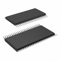
Packaged in 48-Pin TSSOP (DGG)
APPLICATIONS
•
•
•
•
•
•
AdvancedTCA™ (ATCA™) Clock Bus Driver
Clock Distribution
Data and Clock Repeating Over Backplanes
and Cables
Cellular Base Stations
Central Office Switches
Network Switches and Routers
LOGIC DIAGRAM
EN1
EN1
1A
1A
1B
EN2
1B
EN2
EN3
2A
2B
1D
3A
EN3
2A
2B
3A
3B
EN4
4A
4B
1D
3B
EN4
4A
4B
EN5
EN5
5A
5A
5B
5B
EN6
EN6
6A
6B
6A
6B
EN7
7A
2D
EN7
7A
7B
EN8
7B
EN8
8A
8B
SN65MLVD128
8A
8B
SN65MLVD129
Please be aware that an important notice concerning availability, standard warranty, and use in critical applications of Texas
Instruments semiconductor products and disclaimers thereto appears at the end of this data sheet.
AdvancedTCA, ATCA are trademarks of PCI Industrial Computer Manufacturers Group.
PRODUCTION DATA information is current as of publication date.
Products conform to specifications per the terms of the Texas
Instruments standard warranty. Production processing does not
necessarily include testing of all parameters.
Copyright © 2004, Texas Instruments Incorporated
�SN65MLVD128
SN65MLVD129
www.ti.com
SLLS586 – MARCH 2004
These devices have limited built-in ESD protection. The leads should be shorted together or the device placed in conductive foam
during storage or handling to prevent electrostatic damage to the MOS gates.
DESCRIPTION
The SN65MLVD128 and SN65MLVD129 are LVTTL-to-M-LVDS translators/repeaters. Outputs comply with the
M-LVDS standard (TIA/EIA-899) and are optimized for data rates up to 250 Mbps, and clock frequencies up to
125 MHz. The driver outputs have been designed to support multipoint buses presenting loads as low as 30 Ω
and incorporates controlled transition times for backbone operation.
M-LVDS compliant devices allow for 32 nodes on a common bus, providing a high-speed replacement for
RS-485 devices when lower common-mode voltage range and lower output signaling levels are acceptable. The
SN65MLVD128 and SN65MLVD129 provide separate driver enables, allowing for independent control of each
output signal.
Intended applications for these devices include transmission of clock signals from a central clock module, as well
as translation and buffering of data or control signals for transmission through a controlled impedance backplane
or cable.
ORDERING INFORMATION
PART NUMBER
INPUT/OUTPUT CHANNEL
PART MARKING
PACKAGE/CARRIER
SN65MLVD128DGG
1:8
MLVD128
48-Pin TSSOP/Tube
SM65MLVD128DGGR
1:8
MLVD128
48-Pin TSSOP/Tape and Reeled
SN65MLVD129DGG
Dual 1:4
MLVD129
48-Pin TSSOP/Tube
SM65MLVD129DGGR
Dual 1:4
MLVD129
48-Pin TSSOP/Tape and Reeled
PACKAGE DISSIPATION RATINGS
PACKAGE
PCB JEDEC
STANDARD
TA ≤ 25°C
POWER RATING
DERATING FACTOR (1)
ABOVE TA = 25°C
TA = 85°C
POWER RATING
48-DGG
Low-K (2)
1114.6 mW
9.7 mW/°C
533.1 mW
48-DGG
High-K (3)
1824.5 mW
15.9 mW/°C
872.6 mw
(1)
(2)
(3)
This is the inverse of the junction-to-ambient thermal resistance when board mounted and with no air flow.
In accordance with the Low-K thermal metric definitions of EIA/JESD51-3.
In accordance with the High-K thermal metric definitions of EIA/JESD51-7.
ABSOLUTE MAXIMUM RATINGS
over operating free-air temperature range unless otherwise noted (1)
SN65MLVD128, 129
range (2)
VCC
Supply voltage
VI
Input voltage range
D, EN
–0.5 V to 4 V
–0.5 V to 4 V
VO
Output voltage range
A or B
–1.8 V to 4 V
Human Body Model (3)
Electrostatic discharge
A, B
±4 kV
Charged-Device Model (4)
All pins
±1500 V
Machine Model (5)
All pins
200 V
Continuous power dissipation
(1)
(2)
(3)
(4)
(5)
2
±9 kV
All pins
See Dissipation Rating Table
Stresses beyond those listed under absolute maximum ratings may cause permanent damage to the device. These are stress ratings
only, and functional operation of the device at these or any other conditions beyond those indicated under recommended operating
conditions is not implied. Exposure to absolute-maximum-rated conditions for extended periods may affect device reliability.
All voltage values, except differential I/O bus voltages, are with respect to network ground terminal.
Tested in accordance with JEDEC Standard 22, Test Method A114-B.
Tested in accordance with JEDEC Standard 22, Test Method C101-A.
Tested in accordance with JEDEC Standard 22, Test Method A115-A.
Submit Documentation Feedback
�SN65MLVD128
SN65MLVD129
www.ti.com
SLLS586 – MARCH 2004
RECOMMENDED OPERATING CONDITIONS
MIN
NOM
3.3
MAX
UNIT
VCC
Supply voltage
3
3.6
V
VIH
High-level input voltage (1)
2
VCC
V
VIL
Low-level input voltage (2)
0
0.8
V
–1.4
3.8
V
30
55
Ω
250
Mbps
125
MHz
85
°C
Voltage at any bus terminal (separate or common mode) VA or VB
RL
Differential load resistance
1/tUI
Signaling rate
Clock frequency
TA
(1)
(2)
Ambient temperature
–40
In accordance with the High-K thermal metric difinitions of EIA/JESD51-7.
In accordance with the Low-K thermal metric difinitions of EIA/JESD51-3.
DEVICE ELECTRICAL CHARACTERISTICS
over recommended operating conditions unless otherwise noted
PARAMETER
Driver enabled
ICC
Supply current
Driver disabled
PD
(1)
(2)
Device power dissipation
TEST CONDITIONS
EN = VCC, Input = VCC or GND, RL = 50 Ω
MIN (1) TYP (2) MAX
140
mA
45
mA
EN = VCC, Input = VCC or GND, RL = 50 Ω
7
mA
EN = VCC, Input = VCC or GND, RL = No load
7
mA
529
mW
EN = VCC, Input = VCC or GND, RL = No load
VCC = 3.6 V, EN = VCC, CL = 15 pF, RL = 50 Ω,
Input 125 MHz 50 % duty cycle square wave, TA = 85°C
112
UNIT
The algebraic convention, in which the least positive (most negative) limit is designated as minimum is used in this data sheet.
All typical values are at 25°C and with a 3.3-V supply voltage.
Submit Documentation Feedback
3
�SN65MLVD128
SN65MLVD129
www.ti.com
SLLS586 – MARCH 2004
DEVICE ELECTRICAL CHARACTERISTICS
over recommended operating conditions unless otherwise noted
PARAMETER
TEST CONDITIONS
MIN (1) TYP (2)
MAX
UNIT
LVTTL (D, EN) INPUT SPECIFICATIONS
|IIH|
High-level input current
VIH = 2 V or VCC
|IIL|
Low-level input current
VIL = GND or 0.8 V
Ci
Input capacitance
VI = 0.4 sin(30E6πt) + 0.5 V (3)
10
µA
10
µA
5
pF
M-LVDS (A, B) OUTPUT SPECIFICATIONS
|VAB|
Differential output voltage magnitude
480
650
mV
∆|VAB|
Change in differential output voltage magnitude See Figure 2
between logic states
–50
50
mV
VOS(SS)
Steady-state common-mode output voltage
0.8
1.2
V
-50
50
mV
150
mV
0
2.4
V
0
2.4
V
1.2
VSS
V
∆VOS(SS Change in steady-state common-mode output
voltage between logic states
)
VOS(PP)
Peak-to-peak common-mode output voltage
VA(OC)
Maximum steady-state open-circuit output
voltage
See Figure 3
See Figure 7
VB(OC)
Maximum steady-state open-circuit output
voltage
VP(H)
Voltage overshoot, low-to-high level output
VP(L)
Voltage overshoot, high-to-low level output
|IOS|
Differential short-circuit output current
magnitude
See Figure 4
IOZ
High-impedance state output current
–1.4 V ≤ (VA or VB) ≤ 3.8 V,
Other output = 1.2 V
IO(OFF)
Power-off output current
–1.4 V ≤ (VA or VB) ≤ 3.8 V,
Other output = 1.2 V, 0 ≤ VCC≤ 1.5 V
See Figure 5
–0.2 VSS
CA orCB Output capacitance
VI = 0.4 sin(30E6πt) + 0.5 V, (3)
Other input at 1.2 V, driver disabled
CAB
Differential output capacitance
VI = 0.4 sin(30E6πt) V,
Driver disabled
CA/B
Output capacitance balance, (CA/CB)
(1)
(2)
(3)
4
V
24
mA
–20
20
µA
–20
20
µA
3
pF
(3)
2.5
0.99
1.01
The algebraic convention, in which the least positive (most negative) limit is designated as minimum is used in this data sheet.
All typical values are at 25°C and with a 3.3-V supply voltage.
HP4194A impedance analyzer (or equivalent)
Submit Documentation Feedback
pF
�SN65MLVD128
SN65MLVD129
www.ti.com
SLLS586 – MARCH 2004
SWITCHING CHARACTERISTICS
over recommended operating conditions unless otherwise noted
PARAMETER
TEST CONDITIONS
tPLH
Propagation delay time, low-to-high-level output
tPHL
UNIT
1
3
ns
Propagation delay time, high-to-low-level output
1
3
ns
tr
Differential output signal rise time
1
2
ns
tf
Differential output signal fall time
1
2
ns
tsk(p)
Pulse skew (|tpHL– tpLH|)
100
ps
tsk(o)
Output skew
160
ps
tsk(bb)
Bank-to-bank skew (2)
100
ps
tsk(pp)
Part-to-part skew (3)
800
ps
deviation) (4)
See Figure 5
MIN TYP (1) MAX
tjit(per)
Period jitter, rms (1 standard
tjit(c-c)
Cycle-to-cycle jitter (4)
100 MHz clock input, All channels enabled
tjit(pp)
Peak-to-peak jitter (4)
200 Mbps 215-1 PRBS input, All channels
enabled
tPZH
Enable time, high-impedance-to-high-level output
tPZL
Enable time, high-impedance-to-low-level output
tPHZ
Disable time, high-level-to-high-impedance output
tPLZ
Disable time, low-level-to-high-impedance output
(1)
(2)
(3)
(4)
100 MHz clock input, All channels enabled
See Figure 6
See Figure 6
1
46
3
ps
20
ps
110
ps
7
ns
7
ns
7
ns
7
ns
All typical values are at 25°C and with a 3.3-V supply voltage.
tsk(bb), which only applies to the SN65MLVD129, is the magnitude of the difference between the tPLH and tPHL of two outputs of any
bank.
tsk(pp) is the magnitude of the difference in propagation delay times between any specified terminals of two devices when both devices
operate with the same supply voltages, at the same temperature, and have identical packages and test circuits.
Stimulus jitter has been subtracted from the numbers.
Submit Documentation Feedback
5
�SN65MLVD128
SN65MLVD129
www.ti.com
SLLS586 – MARCH 2004
PARAMETER MEASUREMENT INFORMATION
VCC
IA
A
II
VA + VB
D
2
VAB
IB
VY
B
VI
VOS
VB
Figure 1. Driver Voltage and Current Definitions
3.32 kΩ
A
+
_
49.9 Ω
VAB
D
B
-1 V ≤ Vtest ≤ 3.4 V
3.32 kΩ
NOTE: All resistors are 1% tolerance.
Figure 2. Differential Output Voltage Test Circuit
R1
24.9 Ω
A
C1
1 pF
D
≈ 1.3 V
B
≈ 0.7 V
VOS(PP)
B
C2
1 pF
A
R2
24.9 Ω
VOS
C3
2.5 pF
∆VOS(SS)
VOS(SS)
A.
All input pulses are supplied by a generator having the following characteristics: tr or tf≤ 1 ns, frequency = 1 MHz,
duty cycle = 50 ± 5%.
B.
C1, C2 and C3 include instrumentation and fixture capacitance within 2 cm of the D.U.T. and are ±20%.
C.
R1 and R2 are metal film, surface mount, ±1%, and located within 2 cm of the D.U.T.
D.
The measurement of VOS(PP) is made on test equipment with a -3 dB bandwidth of at least 1 GHz.
Figure 3. Test Circuit and Definitions for the Driver Common-Mode Output Voltage
A
IOS
0 V or VCC
+
B
VTest
-1 V or 3.4 V
-
Figure 4. Driver Short-Circuit Test Circuit
6
Submit Documentation Feedback
�SN65MLVD128
SN65MLVD129
www.ti.com
SLLS586 – MARCH 2004
PARAMETER MEASUREMENT INFORMATION (continued)
VCC
VCC/2
Input
0V
tpLH
tpHL
VSS
0.9VSS
VP(H)
Output
0V
VP(L)
0.1V
SS
0 V SS
tf
tr
NOTE: All input pulses are supplied by a generator having the following characteristics: tr or tf≤ 1 ns, frequency = 1 MHz,
duty cycle = 50 ± 5%.
Figure 5. Driver Test Circuit, Timing, and Voltage Definitions for the Differential Output Signal
R1
24.9 Ω
A
GND or VCC
Input
C1
1 pF
D
C2
1 pF
B
EN
C4
Output
0.5 pF
R2
24.9 Ω
VCC
VCC/2
0V
EN
tpZH
tpHZ
∼ 0.6 V
0.1 V
0V
Output With
D at VCC
Output With
D at GND
C3
2.5 pF
tpZL
tpLZ
0V
-0.1 V
∼ -0.6 V
A.
All input pulses are supplied by a generator having the following characteristics: tr or tf≤ 1 ns, frequency = 1 MHz,
duty cycle = 50 ± 5%.
B.
C1, C2, C3, and C4 include instrumentation and fixture capacitance within 2 cm of the D.U.T. and are ±20%.
C.
R1 and R2 are metal film, surface mount, ±1%, and located within 2 cm of the D.U.T.
Figure 6. Driver Enable and Disable Time Circuit and Definitions
A
0 V or VCC
B
VA or VB
1.62 kΩ, ±1%
Figure 7. Driver Maximum Steady State Output Voltage
Submit Documentation Feedback
7
�SN65MLVD128
SN65MLVD129
www.ti.com
SLLS586 – MARCH 2004
PARAMETER MEASUREMENT INFORMATION (continued)
VCC
CLOCK
INPUT
VCC/2
0V
1/f0
Period Jitter
IDEAL
OUTPUT 0 V
VA -VB
VCC
PRBS INPUT
0V
ACTUAL
OUTPUT 0 V
VA -VB
VCC/2
1/f0
Peak to Peak Jitter
VA -VB
tc(n)
tjit(per) = tc(n) -1/f0
OUTPUT 0 V
VA -VB
tjit(pp)
Cycle to Cycle Jitter
OUTPUT
0V
VA - VB
tc(n)
tc(n+1)
tjit(cc) = | tc(n) - tc(n+1) |
A.
All input pulses are supplied by an Agilent 8304A Stimulus System.
B.
The measurement is made on a TEK TDS6604 running TDSJIT3 application software
C.
Period jitter and cycle-to-cycle jitter are measured using a 100 MHz 50 ±1% duty cycle clock input.
D.
Peak-to-peak jitter is measured using a 200 Mbps 215-1 PRBS input.
Figure 8. Driver Jitter Measurement Waveforms
8
Submit Documentation Feedback
�SN65MLVD128
SN65MLVD129
www.ti.com
SLLS586 – MARCH 2004
Table 1. Terminal Functions
PIN
NAME
TYPE
NO.
DESCRIPTION
SN65MLVD128
1D
39
Input
Data inputs for drivers
EN1–EN8
27, 28, 32, 33, 40, 41, 45, 46
Input
Driver enable, active high, individual enables
1A–8A
2, 4, 8, 10, 14, 16, 20, 22
Output
M-LVDS bus noninverting output
1B–8B
3, 5, 9, 11, 15, 17, 21, 23
Output
M-LVDS bus inverting output
GND
6, 12, 18, 24, 25, 26, 31, 37, 38, 43, 44
Power
Circuit ground
VCC
1, 7, 13, 19, 29, 30, 35, 36, 47, 48
Power
Supply voltage
NC
34, 42
N/A
Not connected
SN65MLVD129
1D, 2D
39, 34
Input
Data inputs for drivers
EN1–EN8
27, 28, 32, 33,40, 41, 45, 46
Input
Driver enable, active high, individual enables
1A–8A
2, 4, 8, 10,14, 16, 20, 22
Output
M-LVDS bus noninverting output
1B–8B
3, 5, 9, 11,15, 17, 21, 23
Output
M-LVDS bus inverting output
GND
6, 12, 18, 24, 25, 26, 31, 37, 38, 43, 44
Power
Circuit ground
VCC
1, 7, 13, 19, 29, 30, 35, 36, 47, 48
Power
Supply voltage
NC
42
N/A
Not connected
PIN ASSIGNMENTS
MLVD129DGG
48-TSSOP PACKAGE
(TOP VIEW)
MLVD128DGG
48-TSSOP PACKAGE
(TOP VIEW)
VCC
1A
1B
2A
2B
GND
VCC
3A
3B
4A
4B
GND
VCC
5A
5B
6A
6B
GND
VCC
7A
7B
8A
8B
GND
1
2
3
4
5
6
7
8
9
10
11
12
13
14
15
16
17
18
19
20
21
22
23
24
48
47
46
45
44
43
42
41
40
39
38
37
36
35
34
33
32
31
30
29
28
27
26
25
VCC
VCC
EN1
EN2
GND
GND
NC
EN3
EN4
1D
GND
GND
VCC
VCC
NC
EN5
EN6
GND
VCC
VCC
EN7
EN8
GND
GND
VCC
1A
1B
2A
2B
GND
VCC
3A
3B
4A
4B
GND
VCC
5A
5B
6A
6B
GND
VCC
7A
7B
8A
8B
GND
1
2
3
4
5
6
7
8
9
10
11
12
13
14
15
16
17
18
19
20
21
22
23
24
48
47
46
45
44
43
42
41
40
39
38
37
36
35
34
33
32
31
30
29
28
27
26
25
VCC
VCC
EN1
EN2
GND
GND
NC
EN3
EN4
1D
GND
GND
VCC
VCC
2D
EN5
EN6
GND
VCC
VCC
EN7
EN8
GND
GND
NC - No internal connection
Submit Documentation Feedback
9
�SN65MLVD128
SN65MLVD129
www.ti.com
SLLS586 – MARCH 2004
FUNCTION TABLE
MLVD128 / MLVD129 (1)
(1)
INPUT
ENABLE
D
EN
OUTPUTS
A
B
H
L
H
L
H
H
H
L
OPEN
H
L
H
X
OPEN
Z
Z
X
L
Z
Z
H = high level, L = low level, Z = high impedance, X = Don't care,
OPEN = indeterminate
EQUIVALENT INPUT AND OUTPUT SCHEMATIC DIAGRAMS
DRIVER OUTPUT
DRIVER INPUT AND DRIVER ENABLE
VCC
VCC
400 Ω
D or EN
A or
B
7V
360 kΩ
TYPICAL CHARACTERISTICS
RMS SUPPLY CURRENT
vs
INPUT FREQUENCY
RMS SUPPLY CURRENT
vs
FREE-AIR TEMPERATURE
180
150
VCC = 3.3 V
TA = 25�C
All EN = VCC
RL = 50 �
ICC − RMS Supply Current − mA
ICC − RMS Supply Current − mA
180
120
90
60
VCC = 3.3 V
f = 100 MHz
All EN = VCC
RL = 50 �
150
120
90
60
25
50
75
100
f − Input Frequency − MHz
125
−40
Figure 9.
10
−15
35
60
10
TA − Free-Air Temperature − °C
Figure 10.
Submit Documentation Feedback
85
�SN65MLVD128
SN65MLVD129
www.ti.com
SLLS586 – MARCH 2004
TYPICAL CHARACTERISTICS (continued)
DIFFERENTIAL OUTPUT VOLTAGE MAGNITUDE
vs
INPUT FREQUENCY
PROPAGATION DELAY TIME
vs
FREE-AIR TEMPERATURE
650
2.4
TA = 25�C
EN = VCC
RL = 50 �,
2.3
t pd − Propagation Delay Time − ns
VAB − Differential Output Voltage Magnitude − mV
700
600
VCC = 3.6 V
VCC = 3.3 V
550
VCC = 3 V
500
VCC = 3.3 V
f = 500 kHz
EN = VCC
RL = 50 �
2.2
2.1
tPLH
2
1.9
1.8
tPHL
1.7
450
25
50
75
100
1.6
125
−40
35
Figure 12.
TRANSITION TIME
vs
FREE-AIR TEMPERATURE
PEAK-TO-PEAK JITTER
vs
DATA RATE
60
85
100
VCC = 3.3 V
f = 500 kHz
EN = VCC
RL = 50 �
90
t jit(p-p) − Peak-To-Peak Jitter − ps
t r or t f − Rising or Falling Transition Time − ns
1.8
10
Figure 11.
2
1.9
−15
TA − Free-Air Temperature − °C
f − Input Frequency − MHz
1.7
1.6
tf
1.5
tr
1.4
1.3
1.2
1.1
80
VCC = 3.3 V,
TA = 25�C,
215-1 PRBS NRZ,
All EN = VCC
See Figure 8
70
60
50
40
30
20
1
10
−40
35
−15
60
10
TA − Free-Air Temperature − °C
85
Figure 13.
50
100
150
200
Data Rate − Mbps
250
Figure 14.
Submit Documentation Feedback
11
�SN65MLVD128
SN65MLVD129
www.ti.com
SLLS586 – MARCH 2004
TYPICAL CHARACTERISTICS (continued)
PERIOD JITTER
vs
CLOCK FREQUENCY
CYCLE-TO-CYCLE JITTER
vs
CLOCK FREQUENCY
13
1.0
t jit(per) − Period Jitter − ps
0.8
12
t jit(c-c) − Cycle-To-Cycle Jitter − ps
0.9
VCC = 3.3 V,
TA = 25�C,
Input = Clock
All EN = VCC
See Figure 8
0.7
0.6
0.5
0.4
0.3
0.2
0.1
11
10
9
8
7
6
5
4
3
2
1
0
0
25
50
75
100
f − Clock Frequency − MHz
125
25
50
75
100
f − Clock Frequency − MHz
Figure 15.
12
VCC = 3.3 V,
TA = 25�C,
Input = Clock
All EN = VCC
See Figure 8
Figure 16.
Submit Documentation Feedback
125
�SN65MLVD128
SN65MLVD129
www.ti.com
SLLS586 – MARCH 2004
APPLICATION INFORMATION
CLOCK DISTRIBUTION
SN65MLVD128 Output
SN65MLVD128 Output
Input Source: 19.6608 MHz Clock With 50%
Duty Cycle, VCC = 3.3 V, RL = 50 �, CL = 2.5 pF
Input Source: 61.44 MHz Clock With 50%
Duty Cycle, VCC = 3.3 V, RL = 50 �, CL = 2.5 pF
Output duty cycle = 50.01%.
Vertical scale = 142 mV/div
Horizontal scale = 4 ns/div
Output Duty cycle = 49.97%.
Vertical scale = 142 mV/div
Horizontal scale = 11 ns/div
Figure 17.
Figure 18.
DATA DISTRIBUTION
SN65MLVD128 Output
Input Source: 250 Mbps, 215-1 PRBS,
VCC = 3.3 V, RL = 50 �, CL = 2.5 pF
Vertical scale = 150 mV/div
Horizontal scale = 1.21 ns/div
Figure 19.
Submit Documentation Feedback
13
�PACKAGE OPTION ADDENDUM
www.ti.com
10-Dec-2020
PACKAGING INFORMATION
Orderable Device
Status
(1)
Package Type Package Pins Package
Drawing
Qty
Eco Plan
(2)
Lead finish/
Ball material
MSL Peak Temp
Op Temp (°C)
Device Marking
(3)
(4/5)
(6)
SN65MLVD128DGG
ACTIVE
TSSOP
DGG
48
40
RoHS & Green
NIPDAU
Level-2-260C-1 YEAR
-40 to 85
MLVD128
SN65MLVD128DGGR
ACTIVE
TSSOP
DGG
48
2000
RoHS & Green
NIPDAU
Level-2-260C-1 YEAR
-40 to 85
MLVD128
SN65MLVD129DGG
ACTIVE
TSSOP
DGG
48
40
RoHS & Green
NIPDAU
Level-2-260C-1 YEAR
-40 to 85
MLVD129
SN65MLVD129DGGR
ACTIVE
TSSOP
DGG
48
2000
RoHS & Green
NIPDAU
Level-2-260C-1 YEAR
-40 to 85
MLVD129
(1)
The marketing status values are defined as follows:
ACTIVE: Product device recommended for new designs.
LIFEBUY: TI has announced that the device will be discontinued, and a lifetime-buy period is in effect.
NRND: Not recommended for new designs. Device is in production to support existing customers, but TI does not recommend using this part in a new design.
PREVIEW: Device has been announced but is not in production. Samples may or may not be available.
OBSOLETE: TI has discontinued the production of the device.
(2)
RoHS: TI defines "RoHS" to mean semiconductor products that are compliant with the current EU RoHS requirements for all 10 RoHS substances, including the requirement that RoHS substance
do not exceed 0.1% by weight in homogeneous materials. Where designed to be soldered at high temperatures, "RoHS" products are suitable for use in specified lead-free processes. TI may
reference these types of products as "Pb-Free".
RoHS Exempt: TI defines "RoHS Exempt" to mean products that contain lead but are compliant with EU RoHS pursuant to a specific EU RoHS exemption.
Green: TI defines "Green" to mean the content of Chlorine (Cl) and Bromine (Br) based flame retardants meet JS709B low halogen requirements of