SN65MLVD2
SN65MLVD3
www.ti.com
SLLS767 – NOVEMBER 2006
SINGLE M-LVDS RECEIVERS
FEATURES
APPLICATIONS
•
•
•
•
•
•
•
•
•
•
(1)
Low-Voltage Differential 30-Ω to 55-Ω Line
Receivers for Signaling Rates(1) up to
250Mbps; Clock Frequencies up to 125MHz
SN65MLVD2 Type-1 Receiver Incorporates 25
mV of Input Threshold Hysteresis
SN65MLVD3 Type-2 Receiver Provides 100
mV Offset Threshold to Detect Open-Circuit
and Idle-Bus Conditions
Wide Receiver Input Common-Mode Voltage
Range, –1 V to 3.4 V, Allows 2 V of Ground
Noise
Improved VIT (35 mV)
Meets or Exceeds the M-LVDS Standard
TIA/EIA-899 for Multipoint Topology
High Input Impedance with Low Supply
Voltage
Bus-Pin HBM ESD Protection Exceeds 9 kV
Packaged in 8-Pin SON (DRB) 70% Smaller
Than 8-Pin SOIC
•
•
•
Parallel Multipoint Data and Clock
Transmission via Backplanes and Cables
Cellular Base Stations
Central Office Switches
Network Switches and Routers
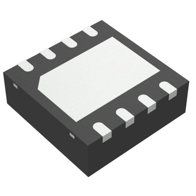
PACKAGE AND PIN-OUT
SN65MLVD2DRB
SN65MLVD3DRB
SON-8
VCC
1
8
VCC
RE
2
7
B
R
3
6
A
GND
4
5
GND
The signaling rate of a line is the number of voltage
transitions that are made per second, expressed in the units
bps (bits per second).
DESCRIPTION
The SN65MLVD2 and SN65MLVD3 are single-channel M-LVDS receivers. These devices are designed in full
compliance with the TIA/EIA-899 (M-LVDS) standard, which are optimized to operate at signaling rates up to
250 Mbps. Each receiver channel is controlled by a receive enable (RE). When RE = low, the corresponding
channel is enabled; when RE = high, the corresponding channel is disabled.
The M-LVDS standard defines two types of receivers, designated as Type-1 and Type-2. Type-1 receivers
(SN65MLVD2) have thresholds centered about zero with 25 mV of hysteresis to prevent output oscillations with
loss of input; Type-2 receivers (SN65MLVD3) implement a failsafe by using an offset threshold. Receiver
outputs are slew rate controlled to reduce EMI and crosstalk effects associated with large current surges.
The devices are characterized for operation from –40°C to 85°C.
Please be aware that an important notice concerning availability, standard warranty, and use in critical applications of Texas
Instruments semiconductor products and disclaimers thereto appears at the end of this data sheet.
PRODUCTION DATA information is current as of publication date.
Products conform to specifications per the terms of the Texas
Instruments standard warranty. Production processing does not
necessarily include testing of all parameters.
Copyright © 2006, Texas Instruments Incorporated
�SN65MLVD2
SN65MLVD3
www.ti.com
SLLS767 – NOVEMBER 2006
TYPICAL APPLICATION
(System Clock - Primary)
(System Clock - Secondary)
User defined frequency
< 100 MHz
19.44 MHz
8 KHz
M-LVDS
Transceiver
M-LVDS
Transceiver
19.44 MHz
8 KHz
M-LVDS
Transceiver
M-LVDS
Transceiver
User defined frequency
< 100 MHz
M-LVDS
Transceiver
80 RT
CLK1A (8 KHz)
80 RT
80 RT
CLK1B (8KHz)
80 RT
80 R
CLK2A (19.44 MHz)
80 R
CLK2B (19.44 MHz)
80 R
80 R
T
T
T
T
80 RT
CLK3A (user defined frequency)
80 RT
80 R
CLK3B (user defined frequency)
80 R
T
M-LVDS
Receivers
CLK1A
8 KHz
M-LVDS
Receivers
CLK1B
8 KHz
M-LVDS
Receivers
CLK2A
19.44 MHz
M-LVDS
Receivers
CLK2B
19.44 MHz
M-LVDS
Receivers
AdvancedTCA Backplane - Synchronized System Clock
Submit Documentation Feedback
M-LVDS
Receivers
CLK3A
CLK3B
User defined frequency
Line Card 1 - N
2
M-LVDS
Transceiver
T
�SN65MLVD2
SN65MLVD3
www.ti.com
SLLS767 – NOVEMBER 2006
These devices have limited built-in ESD protection. The leads should be shorted together or the device placed in conductive foam
during storage or handling to prevent electrostatic damage to the MOS gates.
ORDERING INFORMATION (1)
PART NUMBER
FUNCTION
PART MARKING
PACKAGE / CARRIER
SN65MLVD2DRBT
M-LVDS Type 1 Receiver
MF2
8-Pin SON / Small Tape and Reel
SN65MLVD2DRBR
M-LVDS Type 1 Receiver
MF2
8-Pin SON / Tape and Reel
SN65MLVD3DRBT
M-LVDS Type 2 Receiver
MF3
8-Pin SON / Small Tape and Reel
SN65MLVD3DRBR
M-LVDS Type 2 Receiver
MF3
8-Pin SON / Tape and Reel
(1)
For the most current package and ordering information, see the Package Option Addendum at the end of this document, or see the TI
website at www.ti.com.
ABSOLUTE MAXIMUM RATINGS
over operating free-air temperature range (unless otherwise noted)
VCC
(1)
VALUE
UNIT
–0.5 to 4
V
RE
–0.5 to 4
V
A or B
–1.8 to 4
V
R
–0.3 to 4
V
Supply voltage range (2)
Input voltage range
Output voltage range
Human-body model (3)
Electrostatic discharge
All other pins
±7
A, B
±9
Machine model (4)
All pins
±200
V
Field-induced-charged-device model (5)
All pins
±2
kV
Continuous power dissipation
(1)
(2)
(3)
(4)
(5)
kV
See Dissipation Rating Table
Stresses beyond those listed under absolute maximum ratings may cause permanent damage to the device. These are stress ratings
only, and functional operation of the device at these or any other conditions beyond those indicated under recommended operating
conditions is not implied. Exposure to absolute-maximum-rated conditions for extended periods may affect device reliability.
All voltage values, except differential I/O bus voltages, are with respect to network ground terminal.
Tested in accordance with JEDEC Standard 22, Test Method A114-A. Bus pin stressed with respect to a common connection of GND
and VCC.
Tested in accordance with JEDEC Standard 22 Test Method A115-A.
Tested in accordance with EIA-JEDEC JESD22-C101C.
PACKAGE DISSIPATION RATINGS (1)
PACKAGE
8-SON DRB
(1)
(2)
PCB TYPE
TA≤ 25°C
POWER RATING
DERATING FACTOR (2)
ABOVE TA = 25°C
TA = 85°C
POWER RATING
Low-K
280 mW
2.80 mW/°C
112 mW
High-K
662 mW
6.62 mW/°C
264 mW
The thermal dissipations are in the consideration of soldering down the powerPAD without via on each type of boards.
This is the inverse of the junction-to-ambient thermal resistance when board-mounted and with no air flow.
THERMAL CHARACTERISTICS
PARAMETER
θJB
Junction-to-board thermal resistance
θJC
Junction-to-case thermal resistance
PD
Device power dissipation
TEST CONDITIONS
MIN
TYP
MAX
° C/W
98
RE at 0 V, CL = 15 pF, VID = 400 mV, 125 MHz
Submit Documentation Feedback
UNIT
° C/W
89
90
mW
3
�SN65MLVD2
SN65MLVD3
www.ti.com
SLLS767 – NOVEMBER 2006
RECOMMENDED OPERATING CONDITIONS
over operating free-air temperature range (unless otherwise noted)
MIN
NOM
MAX
VCC
Supply voltage
3
3.3
3.6
V
VIH
High-level input voltage
2
VCC
V
VIL
Low-level input voltage
GND
0.8
V
VA or VB
Voltage at any bus terminal
–1.4
3.8
V
|VID|
Magnitude of differential input voltage
0.035
VCC
V
VIC
Differential common-mode input voltage
–1
RL
Differential load resistance
30
1/tUI
Signaling rate
TA
Operating free-air temperature
3.4
V
Ω
50
–40
UNIT
250
Mbps
85
°C
DEVICE ELECTRICAL CHARACTERISTICS
over recommended operating conditions (unless otherwise noted)
PARAMETER
ICC
(1)
Supply current
TEST CONDITIONS
MIN
TYP (1) MAX
RE at 0 V, CL = 15 pF, VID = 400 mV, 125 MHz
25
UNIT
mA
All typical values are at 25°C and with a 3.3-V supply voltage.
RECEIVER ELECTRICAL CHARACTERISTICS
over recommended operating conditions (unless otherwise noted)
PARAMETER
VIT+
Positive-going differential input voltage
threshold
VIT–
Differential input voltage hysteresis
(VIT+– VIT–)
MIN TYP (1)
MAX
Type 1
35
Type 2
135
Negative-going differential input voltage Type 1
threshold
Type 2
VHYS
See Figure 1, Table 1 and Table 2
–35
UNIT
mV
mV
65
Type 1
25
Type 2
0
mV
VOH
High-level output voltage
IOH = –8 mA
VOL
Low-level output voltage
IOL = 8 mA
IIH
High-level input current
VIH = 2 V to VCC
–10
IIL
Low-level input current
VIL = GND to 0.8 V
–10
IOZ
High-impedance output current
VO = 0 V or VCC
–10
15
µA
IA or IB
Receiver input current
One input (VA or VB) = –1.4 V or 3.8 V,
Other input = 1.2 V
–20
20
µA
IAB
–4
4
µA
–20
20
µA
–4
4
µA
Receiver differential input current (IA– IB)
VA = VB = –1.4 V or 3.8 V
IA(OFF) or
IB(OFF)
Receiver input current
One input (VA or VB) = –1.4 V or 3.8 V,
Other input = 1.2 V, VCC = GND or 1.5
V
IAB(OFF)
Receiver power-off differential input current (IA– IB)
VA = VB = –1.4 V or 3.8 V, VCC = GND
or 1.5 V
CA or CB
Input capacitance
VI = 0.4sin(30E6πt) + 0.5V, (2)
Other input at 1.2 V
CAB
Differential input capacitance
VAB = 0.4sin(30E6πt) + 0.5 V (2)
CA/B
Input capacitance balance, (CA/CB)
(1)
(2)
4
TEST CONDITIONS
2.4
Submit Documentation Feedback
V
µA
µA
3
pF
2.5
0.99
All typical values are at 25°C and with a 3.3-V supply voltage.
HP4194A impedance analyzer (or equivalent)
V
0.4
1.01
pF
�SN65MLVD2
SN65MLVD3
www.ti.com
SLLS767 – NOVEMBER 2006
RECEIVER SWITCHING CHARACTERISTICS
over recommended operating conditions (unless otherwise noted)
PARAMETER
TEST CONDITIONS
MIN TYP (1)
MAX
UNIT
tPLH
Propagation delay time, low-to-high-level output
2
6
ns
tPHL
Propagation delay time, high-to-low-level output
2
6
ns
tr
Output signal rise time
1
2.3
tf
Output signal fall time
CL = 15 pF, See Figure 2
tsk(p)
Pulse skew (|tPHL– tPLH|)
tsk(pp)
Part-to-part skew
tjit(per)
Period jitter, rms (1 standard deviation) (2)
tjit(c-c)
Cycle-to-cycle jitter,
2.3
Type 1
90
210
Type 2
45
250
125 MHz clock input
rms (3)
125 MHz clock
Type 1
Deterministic jitter (2)
tjit(det)
1
Type 2
Type 1
input (4)
250 Mbps 215-1 PRBS input (5)
ps
1
ns
10
ps
8
ps
500
ps
450
ps
8
ps
tjit(ran)
Random jitter (2)
8
ps
tPZH
Enable time, high-impedance-to-high-level output
CL = 15 pF, See Figure 3
15
ns
tPZL
Enable time, high-impedance-to-low-level output
CL = 15 pF, See Figure 3
15
ns
tPHZ
Disable time, high-level-to-high-impedance output
CL = 15 pF, See Figure 3
10
ns
tPLZ
Disable time, low-level-to-high-impedance output
CL = 15 pF, See Figure 3
10
ns
(1)
(2)
(3)
(4)
(5)
Type 2
250 Mbps 215-1 PRBS input (5)
ns
All typical values are at 25°C and with a 3.3-V supply voltage.
Jitter measured by triggering off of the input source to track out the associated input jitter.
Stimulus jitter has been subtracted from the numbers.
Measured over 75K samples
Measured over BER = 10–6.
TERMINAL FUNCTIONS
TERMINAL
NAME
NO.
I/O
DESCRIPTION
A
6
I
M-LVDS Non-inverting input
B
7
I
M-LVDS Inverting input
R
3
O
Data output from receivers
RE
2
I
Receiver enable, active low, enables all receivers
GND
4, 5
Circuit ground
VCC
1, 8
Supply voltage
DEVICE FUNCTION TABLES
TYPE-1 RECEIVER (SN65MLVD2)
INPUTS (1)
(1)
TYPE-2 RECEIVER (SN65MLVD3)
OUTPUT (1)
VID = VA– VB
RE
R
INPUTS (1)
OUTPUT (1)
VID = VA– VB
RE
R
VID ≥ 35 mV
L
H
VID ≥ 135 mV
L
H
–35 mV ≤ VID ≤ 35 mV
L
?
65 mV ≤ VID ≤ 135 mV
L
?
VID ≤– 35 mV
L
L
VID ≤ 65 mV
L
L
X
H
Z
X
H
Z
X
Open
Z
X
Open
Z
Open Circuit
L
?
Open Circuit
L
L
H=high level, L=low level, Z=high impedance, X=Don’t care, ?=indeterminate
Submit Documentation Feedback
5
�SN65MLVD2
SN65MLVD3
www.ti.com
SLLS767 – NOVEMBER 2006
EQUIVALENT INPUT AND OUTPUT SCHEMATIC DIAGRAMS
Receiver Enable
VCC
360 kW
400 W
RE
7V
Receiver Input
VCC
Receiver Output
VCC
100 kW
100 kW
250 kW
250 kW
10 W
R
B
A
10 W
200 kW
200 kW
7V
6
Submit Documentation Feedback
�SN65MLVD2
SN65MLVD3
www.ti.com
SLLS767 – NOVEMBER 2006
PARAMETER MEASUREMENT INFORMATION
IA
A
IO
R
V ID
(V A +V B )/2
V CM
B
VA
VO
IB
VB
Figure 1. Receiver Voltage and Current Definitions
Table 1. Type-1 Receiver Input Threshold Test Voltages
APPLIED VOLTAGES
(1)
RESULTING DIFFERENTIAL
INPUT VOLTAGE
RESULTING
COMMON-MODE INPUT
VOLTAGE
VID
VIC
RECEIVER
OUTPUT (1)
VIA
VIB
2.400
0.000
2.400
1.200
0.000
2.400
– 2.400
1.200
L
3.400
3.365
0.035
3.3825
H
H
3.365
3.400
– 0.035
3.3825
L
–0.965
–1
0.035
–0.9825
H
–1
–0.965
– 0.035
–0.9825
L
H= high level, L = low level, output state assumes receiver is enabled (RE = L)
Table 2. Type-2 Receiver Input Threshold Test Voltages
APPLIED VOLTAGES
(1)
RESULTING DIFFERENTIAL
INPUT VOLTAGE
RESULTING
COMMON-MODE INPUT
VOLTAGE
RECEIVER
OUTPUT (1)
VIA
VIB
VID
VIC
2.400
0.000
2.400
1.200
0.000
2.400
– 2.400
1.200
L
3.400
3.265
0.135
3.3325
H
3.4000
3.335
0.065
3.3675
L
–0.865
–1
0.135
–0.9325
H
–0.935
–1
0.065
–0.9675
L
H
H= high level, L = low level, output state assumes receiver is enabled (RE = L)
Submit Documentation Feedback
7
�SN65MLVD2
SN65MLVD3
www.ti.com
SLLS767 – NOVEMBER 2006
VID
VA
CL
15 pF
VB
VO
VA
1.2 V
VB
0.8 V
VID
0.4 V
0V
-0.4 V
tPHL
tPLH
VO
90%
10%
tf
tr
VOH
VCC
2
VOL
A.
All input pulses are supplied by a generator having the following characteristics: tr or tf ≤ 1 ns, Frequency = 1 MHz,
duty cycle = 50 ± 5%. CL is a combination of a 20%-tolerance, low-loss ceramic, surface-mount capacitor and fixture
capacitance within 2 cm of the D.U.T.
B.
The measurement is made on test equipment with a –3dB bandwidth of at least 1 GHz.
Figure 2. Receiver Timing Test Circuit and Waveforms
8
Submit Documentation Feedback
�SN65MLVD2
SN65MLVD3
www.ti.com
SLLS767 – NOVEMBER 2006
1.2 V
B
RL
499 W
A
CL
15 pF
Inputs
RE
VO
VTEST
VTEST
VCC
0.8 V
A
VCC
VCC
2
0V
RE
tPZL
tPLZ
VO
VCC
VCC
V 2 + 0.5 V
OL
VOL
VTEST
0V
1.6 V
A
VCC
VCC
2
0V
RE
tPZH
tPHZ
VO
VOH
VOH
VCC
2
0V
0.5 V
A.
All input pulses are supplied by a generator having the following characteristics: tr or tf ≤ 1 ns, frequency = 1 MHz,
duty cycle = 50 ± 5%.
B.
RL is 1% tolerance, metal film, surface mount, and located within 2 cm of the D.U.T
C.
CL is the instrumentation and fixture capacitance within 2 cm of the D.U.T. and ±20%. The measurement is made on
test equipment with a –3dB bandwidth of at least 1GHz.
Figure 3. Receiver Enable/Disable Time Test Circuit and Waveforms
Submit Documentation Feedback
9
�SN65MLVD2
SN65MLVD3
www.ti.com
SLLS767 – NOVEMBER 2006
INPUTS
VA - VB
VCM
CLOCK INPUT
VA - VB
0.4 V
1/fo
1.0 V
Period Jitter
IDEAL
OUTPUT
VOH
VCC /2
VOL
VA
1/fo
PRBS INPUT
ACTUAL
OUTPUT
V OH
VB
VCC/2
VOL
Peak to Peak Jitter
VOH
tc(n)
OUTPUT
tjit(per) = | tc(n) - 1/fo |
VCC/2
VOL
Cycle to Cycle Jitter
OUTPUT
t jit(pp)
VOH
VCC /2
VOL
tc(n)
tc(n+1)
tjit(cc) = | tc(n) - tc(n+1)|
A.
All input pulses are supplied by the Agilent 81250 Parallel BERT Stimulus System with plug-in E4832A.
B.
The cycle-to-cycle jitter measurement is made on a TEK TDS6604 running TDSJIT3 application software
C.
Period jitter is measured using a 125-MHz 50 ± 1% duty cycle clock input.
D.
Deterministic jitter and random jitter are measured using a 250-Mbps 215-1 PRBS input
Figure 4. Receiver Jitter Measurement Waveforms
10
Submit Documentation Feedback
�SN65MLVD2
SN65MLVD3
www.ti.com
SLLS767 – NOVEMBER 2006
TYPICAL CHARACTERISTICS
SUPPLY CURRENT
vs
FREQUENCY
RECEIVER (TYPE-1) PROPAGATION DELAY TIME
vs
FREE-AIR TEMPERATURE
6
12
5.5
MLVD3 (Type 2)
PD - Propagation Delay Time - ns
ICC - Supply Current - mA
10
MLVD2 (Type 1)
8
6
4
VCC = 3.3 V,
TA = 25ºC,
VID = 400 mV,
VIC = 1 V
2
50
75
100
f - Frequency - MHz
4
tPLH
3.5
tPHL
3
2
-40
125
-8.75
22.5
53.75
TA - Free-Air Temperature - ºC
Figure 5.
Figure 6.
RECEIVER (TYPE-2) PROPAGATION DELAY TIME
vs
FREE-AIR TEMPERATURE
RECEIVER (TYPE-1) TRANSITION TIME
vs
FREE-AIR TEMPERATURE
5
2.2
VCC = 3.3 V,
f = 1 MHz,
CL = 15 pF
tr/tf - Rising/Falling Transition Time - ns
5.5
85
2.3
6
PD - Propagation Delay Time - ns
4.5
2.5
0
25
5
VCC = 3.3 V,
f = 1 MHz,
CL = 15 pF
4.5
4
tPHL
3.5
tPLH
3
2.5
2.1
VCC = 3.3 V,
f = 1 MHz,
CL = 15 pF
2
1.9
1.8
tr
1.7
1.6
1.5
1.4
tf
1.3
1.2
1.1
2
-40
-8.75
22.5
53.75
TA - Free-Air Temperature - ºC
85
1
-40
Figure 7.
-8.75
22.5
53.75
TA - Free-Air Temperature - ºC
85
Figure 8.
Submit Documentation Feedback
11
�SN65MLVD2
SN65MLVD3
www.ti.com
SLLS767 – NOVEMBER 2006
TYPICAL CHARACTERISTICS (continued)
RECEIVER (TYPE-2) TRANSITION TIME
vs
FREE-AIR TEMPERATURE
RECEIVER (TYPE-1) TRANSITION TIME
vs
OUTPUT LOAD CAPACITOR
2.3
1.8
VCC = 3.3 V,
f = 1 MHz,
CL = 15 pF
2.1
2
1.9
1.8
1.7
tr
1.6
1.5
1.4
tf
1.3
1.2
1.1
1.6
1.5
1.4
tr
1.3
1.2
1.1
1
tf
0.9
0.8
0.7
0.6
1
-40
-8.75
22.5
53.75
TA - Free-Air Temperature - ºC
0.5
85
5
7.5
11
13
CL - Output Load Capacitor - pF
Figure 9.
Figure 10.
RECEIVER (TYPE-2) TRANSITION TIME
vs
OUTPUT LOAD CAPACITOR
ADDED RECEIVER PEAK-TO-PEAK JITTER
vs
SIGNALING RATE
1.8
15
500
VCC = 3.3 V,
f = 1 MHz,
CL = 15 pF
1.6
450
tjit(pp) - Peak-to-Peak Jitter - ps
1.7
tr/tf - Rising/Falling Transition Time - ns
VCC = 3.3 V,
f = 1 MHz,
CL = 15 pF
1.7
tr/tf - Rising/Falling Transition Time - ns
tr/tf - Rising/Falling Transition Time - ns
2.2
1.5
1.4
1.3
tr
1.2
1.1
1
0.9
0.8
tf
0.7
VCC = 3.3 V, TA = 25ºC,
15
2 - 1 PRBS NRZ,
See Figure 4
400
MLVD2 (Type 1)
350
MLVD3 (Type 2)
300
250
200
150
0.6
0.5
5
7.5
11
13
CL - Output Load Capacitor - pF
15
100
50
Figure 11.
12
100
200
150
Signaling Rate - Mbps
Figure 12.
Submit Documentation Feedback
250
�SN65MLVD2
SN65MLVD3
www.ti.com
SLLS767 – NOVEMBER 2006
TYPICAL CHARACTERISTICS (continued)
ADDED RECEIVER PERIOD JITTER
vs
CLOCK FREQUENCY
ADDED RECEIVER CYCLE-TO-CYCLE JITTER
vs
CLOCK FREQUENCY
5
5
tjit(c-c) rms - Cycle-to-Cycle Jitter - ps
VCC = 3.3 V, TA = 25ºC,
See Figure 4
tjit(per) rms - Period Jitter - ps
4
3
2
MLVD2 (Type 1)
MLVD3 (Type 2)
1
0
25
VCC = 3.3 V, TA = 25ºC,
See Figure 4
4
3
MLVD2 (Type 1)
2
1
MLVD3 (Type 2)
0
50
75
100
fCLK - Clock Frequency - MHz
125
25
Figure 13.
75
100
50
fCLK - Clock Frequency - MHz
125
Figure 14.
33.5 mV/div
EYE PATTERNS
666.9 ps/div
Figure 15. SN65MLVD2 Output (VCC = 3.3 V, CL = 15 pF) 250 Mbps 215–1 PRBS
Submit Documentation Feedback
13
�SN65MLVD2
SN65MLVD3
www.ti.com
SLLS767 – NOVEMBER 2006
33.5 mV/div
TYPICAL CHARACTERISTICS (continued)
666.9 ps/div
Figure 16. SN65MLVD3 Output (VCC = 3.3 V, CL = 15 pF) 250 Mbps 215–1 PRBS
14
Submit Documentation Feedback
�PACKAGE OPTION ADDENDUM
www.ti.com
10-Dec-2020
PACKAGING INFORMATION
Orderable Device
Status
(1)
Package Type Package Pins Package
Drawing
Qty
Eco Plan
(2)
Lead finish/
Ball material
MSL Peak Temp
Op Temp (°C)
Device Marking
(3)
(4/5)
(6)
SN65MLVD2DRBR
ACTIVE
SON
DRB
8
3000
RoHS & Green
NIPDAU
Level-2-260C-1 YEAR
-40 to 85
MF2
SN65MLVD2DRBT
ACTIVE
SON
DRB
8
250
RoHS & Green
NIPDAU
Level-2-260C-1 YEAR
-40 to 85
MF2
SN65MLVD3DRBR
ACTIVE
SON
DRB
8
3000
RoHS & Green
NIPDAU
Level-2-260C-1 YEAR
-40 to 85
MF3
SN65MLVD3DRBT
ACTIVE
SON
DRB
8
250
RoHS & Green
NIPDAU
Level-2-260C-1 YEAR
-40 to 85
MF3
(1)
The marketing status values are defined as follows:
ACTIVE: Product device recommended for new designs.
LIFEBUY: TI has announced that the device will be discontinued, and a lifetime-buy period is in effect.
NRND: Not recommended for new designs. Device is in production to support existing customers, but TI does not recommend using this part in a new design.
PREVIEW: Device has been announced but is not in production. Samples may or may not be available.
OBSOLETE: TI has discontinued the production of the device.
(2)
RoHS: TI defines "RoHS" to mean semiconductor products that are compliant with the current EU RoHS requirements for all 10 RoHS substances, including the requirement that RoHS substance
do not exceed 0.1% by weight in homogeneous materials. Where designed to be soldered at high temperatures, "RoHS" products are suitable for use in specified lead-free processes. TI may
reference these types of products as "Pb-Free".
RoHS Exempt: TI defines "RoHS Exempt" to mean products that contain lead but are compliant with EU RoHS pursuant to a specific EU RoHS exemption.
Green: TI defines "Green" to mean the content of Chlorine (Cl) and Bromine (Br) based flame retardants meet JS709B low halogen requirements of


 工商网监
湘ICP备2023018690号
工商网监
湘ICP备2023018690号

