SN74ABT18652
SCAN TEST DEVICE
WITH 18-BIT TRANSCEIVER AND REGISTER
SCBS132B – AUGUST 1992 – REVISED JANUARY 2002
D
D
D
D
Member of the Texas Instruments
Widebus Family
Compatible With IEEE Std 1149.1-1990
(JTAG) Test Access Port and
Boundary-Scan Architecture
Includes D-Type Flip-Flops and Control
Circuitry to Provide Multiplexed
Transmission of Stored and Real-Time Data
Two Boundary-Scan Cells Per I/O for
Greater Flexibility
D
SCOPE Instruction Set
– IEEE Std 1149.1-1990 Required
Instructions, Optional INTEST, and
P1149.1A CLAMP and HIGHZ
– Parallel Signature Analysis at Inputs
With Masking Option
– Pseudorandom Pattern Generation From
Outputs
– Sample Inputs/Toggle Outputs
– Binary Count From Outputs
– Device Identification
– Even-Parity Opcodes
1A2
1A1
1OEBA
GND
1SAB
1CLKAB
TDO
V CC
TMS
1CLKBA
1SBA
1OEAB
GND
1B1
1B2
1B3
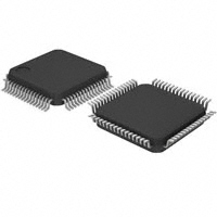
PM PACKAGE
(TOP VIEW)
64 63 62 61 60 59 58 57 56 55 54 53 52 51 50 49
1A3
1A4
1A5
GND
1A6
1A7
1A8
1A9
VCC
2A1
2A2
2A3
GND
2A4
2A5
2A6
1
48
2
47
3
46
4
45
5
44
6
43
7
42
8
41
9
40
10
39
11
38
12
37
13
36
14
35
15
34
16
33
1B4
1B5
1B6
GND
1B7
1B8
1B9
VCC
2B1
2B2
2B3
2B4
GND
2B5
2B6
2B7
2A7
2A8
2A9
GND
2OEBA
2SAB
2CLKAB
TDI
VCC
TCK
2CLKBA
2SBA
GND
2OEAB
2B9
2B8
17 18 19 20 21 22 23 24 25 26 27 28 29 30 31 32
description
This scan test device with an 18-bit bus transceiver and register is a member of the Texas Instruments SCOPE
testability IC family. This device supports IEEE Std 1149.1-1990 boundary scan to facilitate testing of complex
circuit board assemblies. Scan access to the test circuitry is accomplished via the four-wire test access port
(TAP) interface.
Please be aware that an important notice concerning availability, standard warranty, and use in critical applications of
Texas Instruments semiconductor products and disclaimers thereto appears at the end of this data sheet.
SCOPE and Widebus are trademarks of Texas Instruments.
Copyright 2002, Texas Instruments Incorporated
PRODUCTION DATA information is current as of publication date.
Products conform to specifications per the terms of Texas Instruments
standard warranty. Production processing does not necessarily include
testing of all parameters.
POST OFFICE BOX 655303
• DALLAS, TEXAS 75265
1
�SN74ABT18652
SCAN TEST DEVICE
WITH 18-BIT TRANSCEIVER AND REGISTER
SCBS132B – AUGUST 1992 – REVISED JANUARY 2002
description (continued)
In the normal mode, this device is an 18-bit bus transceiver and register that allows for multiplexed transmission
of data directly from the input bus or from the internal registers. It can be used either as two 9-bit transceivers
or one 18-bit transceiver. The test circuitry can be activated by the TAP to take snapshot samples of the data
appearing at the device pins or to perform a self-test on the boundary test cells. Activating the TAP in the normal
mode does not affect the functional operation of the SCOPE bus transceivers and registers.
Data flow in each direction is controlled by clock (CLKAB and CLKBA), select (SAB and SBA), and
output-enable (OEAB and OEBA) inputs. For A-to-B data flow, data on the A bus is clocked into the associated
registers on the low-to-high transition of CLKAB. When SAB is low, real-time A data is selected for presentation
to the B bus (transparent mode). When SAB is high, stored A data is selected for presentation to the B bus
(registered mode). When OEAB is high, the B outputs are active. When OEAB is low, the B outputs are in the
high-impedance state. Control for B-to-A data flow is similar to that for A-to-B data flow but uses CLKBA, SBA,
and OEBA inputs. Since the OEBA input is active-low, the A outputs are active when OEBA is low and are in
the high-impedance state when OEBA is high. Figure 1 illustrates the four fundamental bus-management
functions that can be performed with the SN74ABT18652.
In the test mode, the normal operation of the SCOPE bus transceivers and registers is inhibited, and the test
circuitry is enabled to observe and control the I/O boundary of the device. When enabled, the test circuitry can
perform boundary scan test operations according to the protocol described in IEEE Std 1149.1-1990.
Four dedicated test pins are used to observe and control the operation of the test circuitry: test data input (TDI),
test data output (TDO), test mode select (TMS), and test clock (TCK). Additionally, the test circuitry can perform
other testing functions, such as parallel signature analysis on data inputs and pseudorandom pattern generation
from data outputs. All testing and scan operations are synchronized to the TAP interface.
Additional flexibility is provided in the test mode through the use of two boundary scan cells (BSCs) for each
I/O pin. This allows independent test data to be captured and forced at either bus (A or B). A PSA/COUNT
instruction is also included to ease the testing of memories and other circuits where a binary count addressing
scheme is useful.
ORDERING INFORMATION
TA
PACKAGE†
ORDERABLE
PART NUMBER
TOP-SIDE
MARKING
–40°C to 85°C
LQFP – PM
Tray
SN74ABT18652PM
ABT18652
† Package drawings, standard packing quantities, thermal data, symbolization, and PCB
design guidelines are available at www.ti.com/sc/package.
2
POST OFFICE BOX 655303
• DALLAS, TEXAS 75265
�SN74ABT18652
SCAN TEST DEVICE
WITH 18-BIT TRANSCEIVER AND REGISTER
SCBS132B – AUGUST 1992 – REVISED JANUARY 2002
FUNCTION TABLE
(normal mode, each 9-bit section)
INPUTS
OEAB
OEBA
L
H
L
H
X
H
H
CLKAB
DATA I/O
OPERATION OR FUNCTION
CLKBA
SAB
SBA
A1–A9
B1–B9
L
L
X
X
Input disabled
Input disabled
Isolation
↑
↑
X
X
Input
Input
Store A and B data
↑
L
X
Input
Unspecified†
Store A, hold B
H
↑
↑
X
X‡
X
Input
Output
Store A in both registers
L
X
L
↑
X
Unspecified†
Input
Hold A, store B
L
L
↑
↑
X
X
X‡
Output
Input
Store B in both registers
L
L
X
X
X
L
Output
Input
Real-time B data to A bus
L
L
X
X
X
H
Output
Input
Stored B data to A bus
H
H
X
X
L
X
Input
Output
Real-time A data to B bus
H
H
X
X
H
X
Input
Output
Stored A data to B bus
Output
Stored A data to B bus and
stored B data to A bus
H
L
L
L
H
H
Output
† The data output functions can be enabled or disabled by a variety of level combinations at the OEAB or OEBA inputs. Data input functions are
always enabled, i.e., data at the bus terminals is stored on every low-to-high transition on the clock inputs.
‡ Select control = L: clocks can occur simultaneously.
Select control = H: clocks must be staggered in order to load both registers.
POST OFFICE BOX 655303
• DALLAS, TEXAS 75265
3
�SN74ABT18652
SCAN TEST DEVICE
WITH 18-BIT TRANSCEIVER AND REGISTER
OEAB OEBA
L
L
CLKAB CLKBA SAB
X
X
X
BUS B
BUS A
BUS A
BUS B
SCBS132B – AUGUST 1992 – REVISED JANUARY 2002
SBA
L
OEAB OEBA
H
H
OEBA
H
X
H
CLKAB CLKBA SAB
↑
X
↑
X
↑
↑
X
X
X
SBA
X
X
X
STORAGE FROM
A, B, OR A AND B
OEAB
H
SBA
X
BUS B
OEBA
L
CLKAB
CLKBA
SAB
SBA
X
X
H
H
TRANSFER STORED DATA
TO A AND/OR B
Figure 1. Bus-Management Functions
4
SAB
L
BUS A
BUS A
OEAB
X
L
L
CLKBA
X
REAL-TIME TRANSFER
BUS A TO BUS B
BUS B
REAL-TIME TRANSFER
BUS B TO BUS A
CLKAB
X
POST OFFICE BOX 655303
• DALLAS, TEXAS 75265
�SN74ABT18652
SCAN TEST DEVICE
WITH 18-BIT TRANSCEIVER AND REGISTER
SCBS132B – AUGUST 1992 – REVISED JANUARY 2002
functional block diagram
Boundary-Scan Register
53
1OEAB
VCC
62
1OEBA
55
1CLKBA
54
1SBA
59
1CLKAB
60
1SAB
GND
C1
1D
1A1
63
51
C1
1D
1B1
One of Nine Channels
30
2OEAB
VCC
21
2OEBA
27
2CLKBA
28
2SBA
23
2CLKAB
22
2SAB
GND
C1
1D
2A1
40
10
C1
1D
2B1
One of Nine Channels
Bypass Register
Boundary-Control
Register
Identification
Register
TDI
TMS
TCK
VCC
24
58
Instruction
Register
TDO
VCC
56
26
TAP
Controller
POST OFFICE BOX 655303
• DALLAS, TEXAS 75265
5
�SN74ABT18652
SCAN TEST DEVICE
WITH 18-BIT TRANSCEIVER AND REGISTER
SCBS132B – AUGUST 1992 – REVISED JANUARY 2002
absolute maximum ratings over operating free-air temperature range (unless otherwise noted)†
Supply voltage range, VCC . . . . . . . . . . . . . . . . . . . . . . . . . . . . . . . . . . . . . . . . . . . . . . . . . . . . . . . . . . –0.5 V to 7 V
Input voltage range, VI: Except I/O ports (see Note 1) . . . . . . . . . . . . . . . . . . . . . . . . . . . . . . . . . . –0.5 V to 7 V
I/O ports (see Note 1) . . . . . . . . . . . . . . . . . . . . . . . . . . . . . . . . . . . . . . . . –0.5 V to 5.5 V
Voltage range applied to any output in the high state or power-off state, VO . . . . . . . . . . . . . . –0.5 V to 5.5 V
Current into any output in the low state, IO . . . . . . . . . . . . . . . . . . . . . . . . . . . . . . . . . . . . . . . . . . . . . . . . . . 96 mA
Input clamp current, IIK (VI < 0) . . . . . . . . . . . . . . . . . . . . . . . . . . . . . . . . . . . . . . . . . . . . . . . . . . . . . . . . . . . –18 mA
Output clamp current, IOK (VO < 0) . . . . . . . . . . . . . . . . . . . . . . . . . . . . . . . . . . . . . . . . . . . . . . . . . . . . . . . . –50 mA
Package thermal impedance, θJA (see Note 2) . . . . . . . . . . . . . . . . . . . . . . . . . . . . . . . . . . . . . . . . . . . . . 34°C/W
Storage temperature range, Tstg . . . . . . . . . . . . . . . . . . . . . . . . . . . . . . . . . . . . . . . . . . . . . . . . . . . –65°C to 150°C
† Stresses beyond those listed under “absolute maximum ratings” may cause permanent damage to the device. These are stress ratings only, and
functional operation of the device at these or any other conditions beyond those indicated under “recommended operating conditions” is not
implied. Exposure to absolute-maximum-rated conditions for extended periods may affect device reliability.
NOTES: 1. The input and output negative-voltage ratings may be exceeded if the input and output clamp-current ratings are observed.
2. The package thermal impedance is calculated in accordance with JESD 51-7.
recommended operating conditions (see Note 3)
MIN
MAX
4.5
5.5
UNIT
VCC
VIH
Supply voltage
VIL
VI
Low-level input voltage
IOH
IOL
High-level output current
VCC
–32
mA
Low-level output current
64
mA
∆t/∆v
Input transition rise or fall rate
10
ns/V
High-level input voltage
2
V
0.8
Input voltage
0
V
V
V
TA
Operating free-air temperature
–40
85
°C
NOTE 3: All unused inputs of the device must be held at VCC or GND to ensure proper device operation. Refer to the TI application report,
Implications of Slow or Floating CMOS Inputs, literature number SCBA004.
6
POST OFFICE BOX 655303
• DALLAS, TEXAS 75265
�SN74ABT18652
SCAN TEST DEVICE
WITH 18-BIT TRANSCEIVER AND REGISTER
SCBS132B – AUGUST 1992 – REVISED JANUARY 2002
electrical characteristics over recommended operating free-air temperature range (unless
otherwise noted) (see Note 4)
PARAMETER
VIK
VOH
TEST CONDITIONS
MIN
VCC = 4.5 V,
VCC = 4.5 V,
II = –18 mA
IOH = –3 mA
VCC = 5 V,
IOH = –3 mA
IOH = –24 mA
3
IOH = –32 mA
IOL = 48 mA
2
5V
VCC = 4
4.5
VOL
VCC = 4
4.5
5V
II
VCC = 5
5.5
5V
V,
VCC = 5
5.5
5V
IIH
IIL
VCC = 5.5 V,
VCC = 5.5 V,
VI = VCC,
VI = GND,
IOZH‡
IOZL‡
VCC = 5.5 V,
VCC = 5.5 V,
VO = 2.7 V
VO = 0.5 V
Ioff
ICEX
IO§
VCC = 0,
VCC = 5.5 V,
VI or VO ≤ 5.5 V
VO = 5.5 V
VCC = 5.5 V,
VO = 2.5 V
TYP†
5 5 V,
V IO = 0,
0
VCC = 5.5
VI = VCC or GND
∆ICC#
Ci
VCC = 5.5 V,
VI = 2.5 V or 0.5 V,
0.55
±1
CLK, OEAB, OEBA, S, TCK
±100
A or B ports
Cio
VO = 2.5 V or 0.5 V,
VO = 2.5 V or 0.5 V,
Co
V
µA
TDI, TMS
10
µA
TDI, TMS
–150
µA
50
µA
Outputs high
–50
Outputs low
Outputs disabled
One input at 3.4 V,
V
V
IOL = 64 mA
A or B ports
UNIT
–1.2
2.5
Outputs high
ICC
MAX
–50
µA
±100
µA
50
µA
–200
mA
5.5
38¶
mA
5
Other inputs at VCC or GND
2.5
Control inputs
A or B ports
TDO
mA
3
pF
10
pF
8
pF
NOTE 4: Preliminary specifications based on SPICE analysis
† All typical values are at VCC = 5 V, TA = 25°C.
‡ The parameters IOZH and IOZL include the input leakage current.
§ Not more than one output should be tested at a time, and the duration of the test should not exceed one second.
¶ If both A and B ports are low, ICCL is 76 mA.
# This is the increase in supply current for each input that is at the specified TTL voltage level rather than VCC or GND.
timing requirements over recommended ranges of supply voltage and operating free-air
temperature (unless otherwise noted) (normal mode) (see Note 4 and Figure 2)
MIN
fclock
tw
Clock frequency
CLKAB or CLKBA
Pulse duration
CLKAB or CLKBA high or low
tsu
th
Setup time
A before CLKAB↑ or B before CLKBA↑
Hold time
A after CLKAB↑ or B after CLKBA↑
MAX
UNIT
100
MHz
4
ns
4.5
ns
0
ns
NOTE 4: Preliminary specifications based on SPICE analysis
POST OFFICE BOX 655303
• DALLAS, TEXAS 75265
7
�SN74ABT18652
SCAN TEST DEVICE
WITH 18-BIT TRANSCEIVER AND REGISTER
SCBS132B – AUGUST 1992 – REVISED JANUARY 2002
timing requirements over recommended ranges of supply voltage and operating free-air
temperature (unless otherwise noted) (test mode) (see Note 4 and Figure 2)123
MIN
fclock
tw
tsu
th
td
tr
Clock frequency
TCK
Pulse duration
TCK high or low
Setup time
Hold time
MAX
UNIT
50
MHz
8
A, B, CLK, OEAB, OEBA, or S before TCK↑
4.5
TDI before TCK↑
7.5
TMS before TCK↑
3
A or B after TCK↑
1
CLK, OEAB, OEBA, or S after TCK↑
0
ns
ns
ns
TDI after TCK↑
0.5
TMS after TCK↑
0.5
Delay time
Power up to TCK↑
50
ns
Rise time
VCC power up
1
µs
NOTE 4: Preliminary specifications based on SPICE analysis
switching characteristics over recommended ranges of supply voltage and operating free-air
temperature (unless otherwise noted) (normal mode) (see Note 4 and Figure 2)
PARAMETER
fmax
tPLH
tPHL
tPLH
tPHL
tPLH
tPHL
tPZH
tPZL
tPZH
tPZL
tPHZ
tPLZ
tPHZ
FROM
(INPUT)
TO
(OUTPUT)
CLKAB or CLKBA
A or B
B or A
CLKAB or CLKBA
B or A
SAB or SBA
B or A
OEAB
B
OEBA
A
OEAB
B
POST OFFICE BOX 655303
MAX
100
A
OEBA
tPLZ
NOTE 4: Preliminary specifications based on SPICE analysis
8
MIN
• DALLAS, TEXAS 75265
UNIT
MHz
2
5.4
2
6.6
2.5
8
2.5
7.4
2
7.5
2
8
2.5
8.6
3
9.3
2
6.9
2.5
7.9
3
10.5
2
8.5
3
8.4
1.5
6.5
ns
ns
ns
ns
ns
ns
ns
�SN74ABT18652
SCAN TEST DEVICE
WITH 18-BIT TRANSCEIVER AND REGISTER
SCBS132B – AUGUST 1992 – REVISED JANUARY 2002
switching characteristics over recommended ranges of supply voltage and operating free-air
temperature (unless otherwise noted) (test mode) (see Note 4 and Figure 2)123
PARAMETER
fmax
tPLH
tPHL
tPLH
tPHL
tPZH
tPZL
tPZH
tPZL
tPHZ
tPLZ
tPHZ
FROM
(INPUT)
TO
(OUTPUT)
TCK
MAX
50
TCK↓
A or B
TCK↓
TDO
TCK↓
A or B
TCK↓
TDO
TCK↓
A or B
TCK↓
tPLZ
NOTE 4: Preliminary specifications based on SPICE analysis
POST OFFICE BOX 655303
MIN
TDO
• DALLAS, TEXAS 75265
UNIT
MHz
2.5
13.5
2.5
12.5
2
6.5
2
6.5
4.5
14.2
5
15.5
2
7
3
7.5
4
17
3
16
3
9
3
7.5
ns
ns
ns
ns
ns
ns
9
�SN74ABT18652
SCAN TEST DEVICE
WITH 18-BIT TRANSCEIVER AND REGISTER
SCBS132B – AUGUST 1992 – REVISED JANUARY 2002
PARAMETER MEASUREMENT INFORMATION
7V
500 Ω
From Output
Under Test
Open
S1
GND
CL = 50 pF
(see Note A)
500 Ω
TEST
S1
tPLH/tPHL
tPLZ/tPZL
tPHZ/tPZH
Open
7V
Open
3V
LOAD CIRCUIT
Timing Input
1.5 V
0V
tw
tsu
3V
th
3V
1.5 V
Input
1.5 V
0V
Data Input
1.5 V
0V
VOLTAGE WAVEFORMS
PULSE DURATION
VOLTAGE WAVEFORMS
SETUP AND HOLD TIMES
3V
1.5 V
Input
1.5 V
0V
VOH
1.5 V
Output
1.5 V
VOL
VOH
1.5 V
1.5 V
VOL
VOLTAGE WAVEFORMS
PROPAGATION DELAY TIMES
INVERTING AND NONINVERTING OUTPUTS
1.5 V
1.5 V
0V
tPZL
tPLZ
Output
Waveform 1
S1 at 7 V
(see Note B)
tPLH
tPHL
Output
3V
Output
Control
tPHL
tPLH
1.5 V
Output
Waveform 2
S1 at Open
(see Note B)
1.5 V
3.5 V
VOL + 0.3 V
VOL
tPHZ
tPZH
1.5 V
VOH – 0.3 V
VOH
≈0 V
VOLTAGE WAVEFORMS
ENABLE AND DISABLE TIMES
LOW- AND HIGH-LEVEL ENABLING
NOTES: A. CL includes probe and jig capacitance.
B. Waveform 1 is for an output with internal conditions such that the output is low except when disabled by the output control.
Waveform 2 is for an output with internal conditions such that the output is high except when disabled by the output control.
C. All input pulses are supplied by generators having the following characteristics: PRR ≤ 10 MHz, ZO = 50 Ω, tr ≤ 2.5 ns, tf ≤ 2.5 ns.
D. The outputs are measured one at a time with one transition per measurement.
Figure 2. Load Circuit and Voltage Waveforms
10
POST OFFICE BOX 655303
• DALLAS, TEXAS 75265
�PACKAGE OPTION ADDENDUM
www.ti.com
10-Dec-2020
PACKAGING INFORMATION
Orderable Device
Status
(1)
Package Type Package Pins Package
Drawing
Qty
Eco Plan
(2)
Lead finish/
Ball material
MSL Peak Temp
Op Temp (°C)
Device Marking
(3)
(4/5)
(6)
SN74ABT18652PM
ACTIVE
LQFP
PM
64
160
RoHS & Green
NIPDAU
Level-3-260C-168 HR
-40 to 85
ABT18652
(1)
The marketing status values are defined as follows:
ACTIVE: Product device recommended for new designs.
LIFEBUY: TI has announced that the device will be discontinued, and a lifetime-buy period is in effect.
NRND: Not recommended for new designs. Device is in production to support existing customers, but TI does not recommend using this part in a new design.
PREVIEW: Device has been announced but is not in production. Samples may or may not be available.
OBSOLETE: TI has discontinued the production of the device.
(2)
RoHS: TI defines "RoHS" to mean semiconductor products that are compliant with the current EU RoHS requirements for all 10 RoHS substances, including the requirement that RoHS substance
do not exceed 0.1% by weight in homogeneous materials. Where designed to be soldered at high temperatures, "RoHS" products are suitable for use in specified lead-free processes. TI may
reference these types of products as "Pb-Free".
RoHS Exempt: TI defines "RoHS Exempt" to mean products that contain lead but are compliant with EU RoHS pursuant to a specific EU RoHS exemption.
Green: TI defines "Green" to mean the content of Chlorine (Cl) and Bromine (Br) based flame retardants meet JS709B low halogen requirements of