SN74ABT7819
512 × 18 × 2
CLOCKED BIDIRECTIONAL FIRST-IN, FIRST-OUT MEMORY
SCBS125G – JULY 1992 – REVISED JULY 1998
D
D
D
D
D
D
Member of the Texas Instruments
Widebus Family
Free-Running CLKA and CLKB Can Be
Asynchronous or Coincident
Read and Write Operations Synchronized
to Independent System Clocks
Two Separate 512 × 18 Clocked FIFOs
Buffering Data in Opposite Directions
IRA and ORA Synchronized to CLKA
IRB and ORB Synchronized to CLKB
D
D
D
D
D
D
Microprocessor Interface Control Logic
Programmable Almost-Full/Almost-Empty
Flag
Fast Access Times of 9 ns With a 50-pF
Load and Simultaneous Switching Data
Outputs
Data Rates up to 100 MHz
Advanced BiCMOS Technology
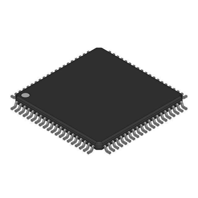
Package Options Include 80-Pin Quad Flat
(PH) and 80-Pin Thin Quad Flat (PN)
Packages
CSA
W/RA
GND
WENA
CLKA
RENA
ORA
VCC
VCC
ORB
RENB
CLKB
WENB
GND
W/RB
CSB
PH PACKAGE
(TOP VIEW)
80 79 78 77 76 75 74 73 72 71 70 69 68 67 66 65
RSTA
PENA
AF/AEA
HFA
IRA
GND
A0
A1
VCC
A2
A3
GND
A4
A5
GND
A6
A7
GND
A8
A9
VCC
A10
A11
GND
64
63
62
61
60
59
58
57
56
55
54
53
52
51
50
49
48
47
46
45
44
43
42
41
1
2
3
4
5
6
7
8
9
10
11
12
13
14
15
16
17
18
19
20
21
22
23
24
RSTB
PENB
AF/AEB
HFB
IRB
GND
B0
B1
VCC
B2
B3
GND
B4
B5
GND
B6
B7
GND
B8
B9
VCC
B10
B11
GND
A12
A13
V CC
A14
A15
GND
A16
A17
B17
B16
GND
B15
B14
VCC
B13
B12
25 26 27 28 29 30 31 32 33 34 35 36 37 38 39 40
Please be aware that an important notice concerning availability, standard warranty, and use in critical applications of
Texas Instruments semiconductor products and disclaimers thereto appears at the end of this data sheet.
Widebus is a trademark of Texas Instruments Incorporated.
Copyright 1998, Texas Instruments Incorporated
PRODUCTION DATA information is current as of publication date.
Products conform to specifications per the terms of Texas Instruments
standard warranty. Production processing does not necessarily include
testing of all parameters.
POST OFFICE BOX 655303
• DALLAS, TEXAS 75265
1
�SN74ABT7819
512 × 18 × 2
CLOCKED BIDIRECTIONAL FIRST-IN, FIRST-OUT MEMORY
SCBS125G – JULY 1992 – REVISED JULY 1998
RENB
CLKB
WENB
GND
W/RB
CSB
RSTB
PENB
PENA
RSTA
CSA
W/RA
GND
WENA
CLKA
RENA
ORA
VCC
VCC
ORB
PN PACKAGE
(TOP VIEW)
80 79 78 77 76 75 74 73 72 71 70 69 68 67 66 65 64 63 62 61
AF/AEA
HFA
IRA
GND
A0
A1
VCC
A2
A3
GND
A4
A5
GND
A6
A7
GND
A8
A9
VCC
A10
1
60
2
59
3
58
4
57
5
56
6
55
7
54
8
53
9
52
10
51
11
50
12
49
13
48
14
47
15
46
16
45
17
44
18
43
19
42
20
41
AF/AEB
HFB
IRB
GND
B0
B1
VCC
B2
B3
GND
B4
B5
GND
B6
B7
GND
B8
B9
VCC
B10
A11
GND
A12
A13
V CC
A14
A15
GND
A16
A17
B17
B16
GND
B15
B14
V CC
B13
B12
GND
B11
21 22 23 24 25 26 27 28 29 30 31 32 33 34 35 36 37 38 39 40
description
A FIFO memory is a storage device that allows data to be written into and read from its array at independent
data rates. The SN74ABT7819 is a high-speed, low-power BiCMOS bidirectional clocked FIFO memory. Two
independent 512 × 18 dual-port SRAM FIFOs on the chip buffer data in opposite directions. Each FIFO has flags
to indicate empty and full conditions, a half-full flag, and a programmable almost-full/almost-empty flag.
The SN74ABT7819 is a clocked FIFO, which means each port employs a synchronous interface. All data
transfers through a port are gated to the low-to-high transition of a continuous (free-running) port clock by enable
signals. The continuous clocks for each port are independent of one another and can be asynchronous or
coincident. The enables for each port are arranged to provide a simple bidirectional interface between
microprocessors and/or buses with synchronous control.
The state of the A0–A17 outputs is controlled by CSA and W/RA. When both CSA and W/RA are low, the outputs
are active. The A0–A17 outputs are in the high-impedance state when either CSA or W/RA is high. Data is
written to FIFOA–B from port A on the low-to-high transition of CLKA when CSA is low, W/RA is high, WENA
is high, and the IRA flag is high. Data is read from FIFOB–A to the A0–A17 outputs on the low-to-high transition
of CLKA when CSA is low, W/RA is low, RENA is high, and the ORA flag is high.
2
POST OFFICE BOX 655303
• DALLAS, TEXAS 75265
�SN74ABT7819
512 × 18 × 2
CLOCKED BIDIRECTIONAL FIRST-IN, FIRST-OUT MEMORY
SCBS125G – JULY 1992 – REVISED JULY 1998
description (continued)
The state of the B0–B17 outputs is controlled by CSB and W/RB. When both CSB and W/RB are low, the outputs
are active. The B0–B17 outputs are in the high-impedance state when either CSB or W/RB is high. Data is
written to FIFOB–A from port B on the low-to-high transition of CLKB when CSB is low, W/RB is high, WENB
is high, and the IRB flag is high. Data is read from FIFOA–B to the B0–B17 outputs on the low-to-high transition
of CLKB when CSB is low, W/RB is low, RENB is high, and the ORB flag is high.
The setup- and hold-time constraints for the chip selects (CSA, CSB) and write/read selects (W/RA, W/RB)
enable write and read operations on memory and are not related to the high-impedance control of the data
outputs. If a port read enable (RENA or RENB) and write enable (WENA or WENB) are set low during a clock
cycle, the chip select and write/read select can switch at any time during the cycle to change the state of the
data outputs.
The input-ready (IR) and output-ready (OR) flags of a FIFO are two-stage synchronized to the port clocks for
use as reliable control signals. CLKA synchronizes the status of the input-ready flag of FIFOA–B (IRA) and the
output-ready flag of FIFOB–A (ORA). CLKB synchronizes the status of the input-ready flag of FIFOB–A (IRB)
and the output-ready flag of FIFOA–B (ORB). When the IR flag of a port is low, the FIFO receiving input from
the port is full and writes are disabled to its array. When the OR flag of a port is low, the FIFO that outputs data
to the port is empty and reads from its memory are disabled. The first word loaded to an empty memory is sent
to the FIFO output register at the same time its OR flag is asserted (high). When the memory is read empty and
the OR flag is forced low, the last valid data remains on the FIFO outputs until the OR flag is asserted (high)
again. In this way, a high on the OR flag indicates new data is present on the FIFO outputs.
The SN74ABT7819 is characterized for operation from 0°C to 70°C.
Function Tables
PORT A
SELECT INPUTS
CLKA
CSA
W/RA
X
H
↑
L
↑
L
L
A0 A17
A0–A17
PORT A OPERATION
PORT-A
WENA
RENA
X
X
X
High Z
None
H
H
X
High Z
Write A0–A17 to FIFOA–B
X
H
Active
Read FIFOB–A to A0–A17
B0 B17
B0–B17
PORT B OPERATION
PORT-B
None
PORT B
SELECT INPUTS
CLKB
CSB
W/RB
WENB
RENB
X
H
X
X
X
High Z
↑
L
H
H
X
High Z
Write B0–B17 to FIFOB–A
↑
L
L
X
H
Active
Read FIFOA–B to B0–B17
POST OFFICE BOX 655303
• DALLAS, TEXAS 75265
3
�SN74ABT7819
512 × 18 × 2
CLOCKED BIDIRECTIONAL FIRST-IN, FIRST-OUT MEMORY
SCBS125G – JULY 1992 – REVISED JULY 1998
logic symbol†
CLKA
CSA
W/RA
76
CLOCK A
&
80
OE1
79
77
&
RENA
75
1
RSTA
PENA
IRA
ORA
HFA
AF/AEA
A0
A1
A2
A3
A4
A5
A6
A7
A8
A9
A10
A11
A12
A13
A14
A15
A16
A17
2
5
74
4
3
7
CLOCK B
&
CLKB
65
OE2
66
WRITE
ENABLE
FIFOA–B
WRITE
ENABLE
FIFOB–A
&
READ
ENABLE
FIFOB–A
READ
ENABLE
FIFOA–B
&
RESET FIFO A–B
PROGRAM ENABLE
FIFO A–B
INPUT-READY
PORT A
OUTPUT-READY
PORT A
HALF-FULL
FIFOA–B
ALMOST-FULL/EMPTY
FIFOA–B
68
70
RESET FIFO B–A
PROGRAM ENABLE
FIFO B–A
INPUT-READY
PORT B
OUTPUT-READY
PORT B
HALF-FULL
FIFOB–A
ALMOST-FULL/EMPTY
FIFOB–A
0
0
8
64
63
60
71
61
62
58
57
10
55
11
54
13
52
14
51
16
49
17
48
19
1
20
46
2
Data
45
Data
22
43
23
42
25
40
26
39
28
37
29
36
31
34
32
33
17
17
† This symbol is in accordance with ANSI/IEEE Std 91-1984 and IEC Publication 617-12.
Pin numbers shown are for the PH package.
4
69
CSB
W/RB
&
WENA
Φ
FIFO 512 × 18 × 2
SN74ABT7819
POST OFFICE BOX 655303
• DALLAS, TEXAS 75265
WENB
RENB
RSTB
PENB
IRB
ORB
HFB
AF/AEB
B0
B1
B2
B3
B4
B5
B6
B7
B8
B9
B10
B11
B12
B13
B14
B15
B16
B17
�SN74ABT7819
512 × 18 × 2
CLOCKED BIDIRECTIONAL FIRST-IN, FIRST-OUT MEMORY
SCBS125G – JULY 1992 – REVISED JULY 1998
functional block diagram
PENA
RENA
WENA
CSA
W/RA
CLKA
RSTA
Port-A
Control
Logic
Read
Pointer
18
Register
512 × 18
Dual-Port SRAM
FIFOB–A
Register
18
18
Write
Pointer
Flag
Logic
FIFOB–A
ORA
IRB
AF/AEB
HFB
8
A0–A17
B0–B17
8
IRA
AF/AEA
HFA
Flag
Logic
FIFOA–B
ORB
Write
Pointer
18
Register
512 × 18
Dual-Port SRAM
FIFOA–B
Register
Read
Pointer
Port-B
Control
Logic
RSTB
CLKB
CSB
W/RB
WENB
RENB
PENB
POST OFFICE BOX 655303
• DALLAS, TEXAS 75265
5
�SN74ABT7819
512 × 18 × 2
CLOCKED BIDIRECTIONAL FIRST-IN, FIRST-OUT MEMORY
SCBS125G – JULY 1992 – REVISED JULY 1998
enable logic diagram (positive logic)
CSA
W/RA
WENA
WEN FIFOA–B
A0–A17 (output enable)
REN FIFOB–A
RENA
CSB
W/RB
WENB
WEN FIFOB–A
B0–B17 (output enable)
REN FIFOA–B
RENB
Terminal Functions
TERMINAL†
NAME
NO.
A0–A17
7–8, 10–11,
13–14, 16–17,
19–20, 22–23,
25–26, 28–29,
31–32
AF/AEA
3
I/O
DESCRIPTION
I/O
Port-A data. The 18-bit bidirectional data port for side A.
O
FIFOA–B almost-full/almost-empty flag. Depth offsets can be programmed for AF/AEA or the default
value of 128 can be used for both the almost-empty offset (X) and the almost-full offset (Y). AF/AEA is
high when X or fewer words or (512 – Y) or more words are stored in FIFOA–B. AF/AEA is forced high
when FIFOA–B is reset.
AF/AEB
62
O
FIFOB–A almost-full/almost-empty flag. Depth offsets can be programmed for AF/AEB or the default
value of 128 can be used for both the almost-empty offset (X) and the almost-full offset (Y). AF/AEB is
high when X or fewer words or (512 – Y) or more words are stored in FIFOB–A. AF/AEB is forced high
when FIFOB–A is reset.
B0–B17
58–57, 55–54,
52–51, 49–48,
46–45, 43–42,
40–39, 37–36,
34–33
I/O
Port-B data. The 18-bit bidirectional data port for side B.
CLKA
76
I
Port-A clock. CLKA is a continuous clock that synchronizes all data transfers through port A to its
low-to-high transition and can be asynchronous or coincident to CLKB.
CLKB
69
I
Port-B clock. CLKB is a continuous clock that synchronizes all data transfers through port B to its
low-to-high transition and can be asynchronous or coincident to CLKA.
CSA
80
I
Port-A chip select. CSA must be low to enable a low-to-high transition of CLKA to either write data from
A0–A17 to FIFOA–B or read data from FIFOB–A to A0–A17. The A0–A17 outputs are in the
high-impedance state when CSA is high.
CSB
65
I
Port-B chip select. CSB must be low to enable a low-to-high transition of CLKB to either write data from
B0–B17 to FIFOB–A or read data from FIFOA–B to B0–B17. The B0–B17 outputs are in the
high-impedance state when CSB is high.
† Terminals listed are for the PH package.
6
POST OFFICE BOX 655303
• DALLAS, TEXAS 75265
�SN74ABT7819
512 × 18 × 2
CLOCKED BIDIRECTIONAL FIRST-IN, FIRST-OUT MEMORY
SCBS125G – JULY 1992 – REVISED JULY 1998
Terminal Functions (Continued)
TERMINAL†
NAME
NO.
I/O
DESCRIPTION
HFA
4
O
FIFOA–B half-full flag. HFA is high when FIFOA–B contains 256 or more words and is low when
FIFOA–B contains 255 or fewer words. HFA is set low after FIFOA–B is reset.
HFB
61
O
FIFOB–A half-full flag. HFB is high when FIFOB–A contains 256 or more words and is low when
FIFOB–A contains 255 or fewer words. HFB is set low after FIFOB–A is reset.
IRA
5
O
Port-A input-ready flag. IRA is synchronized to the low-to-high transition of CLKA. When IRA is low,
FIFOA–B is full and writes to its array are disabled. IRA is set low during a FIFOA–B reset and is set high
on the second low-to-high transition of CLKA after reset.
IRB
60
O
Port-B input-ready flag. IRB is synchronized to the low-to-high transition of CLKB. When IRB is low,
FIFOB–A is full and writes to its array are disabled. IRB is set low during a FIFOB–A reset and is set high
on the second low-to-high transition of CLKB after reset.
O
Port-A output-ready flag. ORA is synchronized to the low-to-high transition of CLKA. When ORA is low,
FIFOB–A is empty and reads from its array are disabled. The last valid word remains on the FIFOB–A
outputs when ORA is low. Ready data is present for the A0–A17 outputs when ORA is high. ORA is set
low during a FIFOB–A reset and goes high on the third low-to-high transition of CLKA after the first word
is loaded to an empty FIFOB–A.
ORA
74
ORB
71
O
Port-B output-ready flag. ORB is synchronized to the low-to-high transition of CLKB. When ORB is low,
FIFOA–B is empty and reads from its array are disabled. The last valid word remains on the FIFOA–B
outputs when ORB is low. Ready data is present for the B0–B17 outputs when ORB is high. ORB is set
low during a FIFOA–B reset and goes high on the third low-to-high transition of CLKB after the first word
is loaded to an empty FIFOA–B.
PENA
2
I
AF/AEA program enable. After FIFOA–B is reset and before a word is written to its array, the binary value
on A0–A7 is latched as an AF/AEA offset when PENA is low and CLKA is high.
PENB
63
I
AF/AEB program enable. After FIFOB–A is reset and before a word is written to its array, the binary value
on B0–B7 is latched as an AF/AEB offset when PENB is low and CLKB is high.
RENA
75
I
Port-A read enable. A high level on RENA enables data to be read from FIFOB–A on the low-to-high
transition of CLKA when CSA is low, W/RA is low, and ORA is high.
RENB
70
I
Port-B read enable. A high level on RENB enables data to be read from FIFOA–B on the low-to-high
transition of CLKB when CSB is low, W/RB is low, and ORB is high.
RSTA
1
I
FIFOA–B reset. To reset FIFOA–B, four low-to-high transitions of CLKA and four low-to-high transitions
of CLKB must occur while RSTA is low. This sets HFA low, IRA low, ORB low, and AF/AEA high.
RSTB
64
I
FIFOB–A reset. To reset FIFOB–A, four low-to-high transitions of CLKA and four low-to-high transitions
of CLKB must occur while RSTB is low. This sets HFB low, IRB low, ORA low, and AF/AEB high.
WENA
77
I
Port-A write enable. A high level on WENA enables data on A0–A17 to be written into FIFOA–B on the
low-to-high transition of CLKA when W/RA is high, CSA is low, and IRA is high.
WENB
68
I
Port-B write enable. A high level on WENB enables data on B0–B17 to be written into FIFOB–A on the
low-to-high transition of CLKB when W/RB is high, CSB is low, and IRB is high.
I
Port-A write/read select. A high on W/RA enables A0–A17 data to be written to FIFOA–B on a low-to-high
transition of CLKA when WENA is high, CSA is low, and IRA is high. A low on W/RA enables data to be
read from FIFOB–A on a low-to-high transition of CLKA when RENA is high, CSA is low, and ORA is high.
The A0–A17 outputs are in the high-impedance state when W/RA is high.
I
Port-B write/read select. A high on W/RB enables B0–B17 data to be written to FIFOB–A on a low-to-high
transition of CLKB when WENB is high, CSB is low, and IRB is high. A low on W/RB enables data to be
read from FIFOA–B on a low-to-high transition of CLKB when RENB is high, CSB is low, and ORB is high.
The B0–B17 outputs are in the high-impedance state when W/RB is high.
W/RA
W/RB
79
66
† Terminals listed are for the PH package.
POST OFFICE BOX 655303
• DALLAS, TEXAS 75265
7
�SN74ABT7819
512 × 18 × 2
CLOCKED BIDIRECTIONAL FIRST-IN, FIRST-OUT MEMORY
SCBS125G – JULY 1992 – REVISED JULY 1998
CLKA
1
CLKB
1
2
3
2
4
3
1
2
4
RSTA
ÎÎÎÎÎÎÎÎÎÎÎÎ
ÎÎÎÎÎÎÎÎÎÎÎÎ
ÎÎÎÎÎÎÎÎÎÎÎÎÎÎÎÎ
ÎÎÎÎÎÎÎÎÎÎÎÎÎÎÎÎ
ÎÎÎÎÎÎÎÎÎÎÎÎÎÎÎÎ
ÎÎÎÎÎ
ÎÎÎÎÎ
ÏÏÏÏÏ
ÏÏÏÏÏ
ÏÏÏÏÏ
IRA
ORB
HFA
AF/AEA
Figure 1. Reset Cycle for FIFOA–B†
† FIFOB–A is reset in the same manner.
CLKA
1
IRA
0
CSA
ÌÌÌÌÌ
ÌÌÌÌÌÌÌ
ÌÌ
ÌÌÌÌÌ
ÌÌÌÌÌÌÌ
ÌÌ
ÌÌÌÌÌÌÌÌ
ÌÌÌÌÌÌ
ÌÌÌÌÌÌÌÌÌÌÌ
ÌÌÌÌÌÌ
ÌÌÌ
ÌÌÌÌÌÌÌÌ
ÌÌÌÌÌÌ
ÌÌÌÌÌÌÌÌÌÌÌ
ÌÌÌÌÌÌ
ÌÌÌ
ÌÌÌÌÌÌÌÌ
ÌÌÌÌÌÌ ÌÌÌÌÌÌ
ÌÌÌ ÌÌÌÌÌÌÌÌÌÌÌ
ÌÌÌÌÌÌÌÌ ÌÌÌÌÌÌ
ÌÌÌ ÌÌÌ
ÌÌ
ÌÌÌÌÌÌ ÌÌÌ ÌÌÌÌÌÌÌÌ ÌÌÌ ÌÌ
W/RA
WENA
A0–A17
Word 1‡
Word 2‡
Word 3‡
‡ Written to FIFOA–B
Figure 2. Write Timing – Port A
8
POST OFFICE BOX 655303
• DALLAS, TEXAS 75265
Word 4‡
�SN74ABT7819
512 × 18 × 2
CLOCKED BIDIRECTIONAL FIRST-IN, FIRST-OUT MEMORY
SCBS125G – JULY 1992 – REVISED JULY 1998
CLKB
1
IRB
0
CSB
ÌÌÌÌÌÌ
ÌÌÌÌÌÌÌÌ
ÌÌÌ
ÌÌÌÌÌÌ
ÌÌÌÌÌÌÌÌ
ÌÌÌ
ÌÌÌÌÌÌÌÌÌÌÌÌÌÌÌÌÌÌÌÌÌÌÌ
ÌÌÌÌÌÌÌÌÌ
ÌÌÌÌÌÌÌÌÌÌÌÌÌÌÌÌÌÌÌÌÌÌÌ
ÌÌÌÌÌÌÌÌÌ
ÌÌÌÌÌÌÌÌ
ÌÌÌÌÌ
ÌÌÌÌÌÌÌÌÌÌ
ÌÌÌÌÌÌ
ÌÌÌ
ÌÌÌÌÌÌ ÌÌÌ ÌÌÌÌÌÌÌÌ ÌÌÌ ÌÌÌ
ÌÌÌÌÌÌ ÌÌÌ ÌÌÌÌÌÌÌÌ ÌÌÌ ÌÌÌ
W/RB
WENB
B0–B17
Word 1†
Word 2†
Word 3†
Word 4†
† Written to FIFOB–A
Figure 3. Write Timing – Port B
POST OFFICE BOX 655303
• DALLAS, TEXAS 75265
9
�SN74ABT7819
512 × 18 × 2
CLOCKED BIDIRECTIONAL FIRST-IN, FIRST-OUT MEMORY
SCBS125G – JULY 1992 – REVISED JULY 1998
CLKA
1
CSA
0
1
W/RA
ÏÏÏÏÏÎÎÎÎÎ
ÏÏÏÏÏ
ÎÎÎÎÎ
ÌÌÌÌÌ ÌÌÌÌÌÌÌÌÌÌÌÌÌÌÌÌÌÌÌÌÌÌÌÌ
ÌÌÌÌÌ ÌÌÌÌÌÌÌÌÌÌÌÌÌÌÌÌÌÌÌÌÌÌÌÌ
WENA
tsu
A0–A17
CLKB
W1
1
2
3
ORB
tpd
tpd
CSB
W/RB
ÏÏÏÏÏÏÏÏÏÏÏÏÏÏÏÏÏÏÏÏ
ÎÎÎÎÎÎÎÎÎÎÎ
ÏÏÏÏÏÏÏÏÏÏÏÏÏÏÏÏÏÏÏÏ
ÎÎÎÎÎÎÎÎÎÎÎ
ÌÌÌÌÌÌÌÌÌÌÌÌÌÌÌÌ
ÌÌÌÌÌÌÌÌÌÌÌÌÌÌÌÌ
RENB
tpd
B0–B17
W1 From FIFOA–B
Figure 4. ORB-Flag Timing and First Data-Word Fall-Through When FIFOA–B Is Empty†
† Operation of FIFOB–A is identical to that of FIFOA–B.
10
POST OFFICE BOX 655303
• DALLAS, TEXAS 75265
0
�SN74ABT7819
512 × 18 × 2
CLOCKED BIDIRECTIONAL FIRST-IN, FIRST-OUT MEMORY
SCBS125G – JULY 1992 – REVISED JULY 1998
CLKB
1
CSB
0
1
W/RB
RENB
0
ÏÏÏ ÎÎÎÎ
ÏÏÏ ÎÎÎÎ
From FIFOA–B
B0–B17
CLKA
1
2
IRA
tpd
tpd
1
CSA
0
WENA
ÏÏÏÏÏÏÏÏÏÏÏÏÏÏÏÎÎÎÎÎÎÎÎÎÎÎÎÎÎÎ
ÏÏÏÏÏÏÏÏÏÏÏÏÏÏÏÎÎÎÎÎÎÎÎÎÎÎÎÎÎÎ
1
W/RA
0
A0–A17
ÌÌÌÌÌÌÌÌÌÌÌÌÌÌÌ ÌÌÌÌÌÌÌÌÌÌÌÌÌ
ÌÌÌÌÌÌÌÌÌÌÌÌÌÌÌ ÌÌÌÌÌÌÌÌÌÌÌÌÌ
To FIFOA–B
Figure 5. Write-Cycle and IRA-Flag Timing When FIFOA–B Is Full†
† Operation of FIFOB–A is identical to that of FIFOA–B.
POST OFFICE BOX 655303
• DALLAS, TEXAS 75265
11
�SN74ABT7819
512 × 18 × 2
CLOCKED BIDIRECTIONAL FIRST-IN, FIRST-OUT MEMORY
SCBS125G – JULY 1992 – REVISED JULY 1998
CLKA
1
ORA
0
CSA
ÎÎÎÎ
ÏÏÏÏÏÏÏ
ÎÎÎÎ
ÏÏÏÏÏÏÏ
ÎÎÎÎ
ÏÏÏÏÏÏÏ
ÌÌÌÌÌÌÌÌÌÌÌÌÌÌÌÌÌÌÌÌÌÌÌÌÌÌÌÌÌÌ
ÌÌÌÌÌÌÌÌÌÌÌÌÌÌÌÌÌÌÌÌÌÌÌÌÌÌÌÌÌÌ
W/RA
RENA
tpd
ten
Word 1†
A0–A17
tdis
Word 2†
Word 3†
Word 4†
† Read from FIFOB–A
Figure 6. Read Timing – Port A
CLKB
1
ORB
0
CSB
ÎÎÎÎ
ÏÏÏÏÏÏÏ
ÎÎÎÎ
ÏÏÏÏÏÏÏ
ÌÌÌÌÌÌÌÌÌÌÌÌÌÌÌÌÌÌÌÌÌÌÌÌÌÌÌÌÌÌ
ÌÌÌÌÌÌÌÌÌÌÌÌÌÌÌÌÌÌÌÌÌÌÌÌÌÌÌÌÌÌ
W/RB
RENB
ten
B0–B17
tpd
Word 1‡
tdis
Word 2‡
Word 3‡
‡ Read from FIFOA–B
Figure 7. Read Timing – Port B
12
POST OFFICE BOX 655303
• DALLAS, TEXAS 75265
Word 4‡
�CLKA
WENA
ÌÌÌ
ÌÌÌÌÌÌ
ÌÌÌ
ÌÌÌÌÌÌ
ÌÌÌÌÌÌ
ÌÌÌ
ÌÌÌÌÌÌ
ÌÌÌÌÌÌ
ÌÌÌ
ÌÌÌ
ÌÌÌ
ÌÌÌ
ÌÌÌÌÌÌ
ÌÌÌ
ÌÌÌÌÌÌ
ÌÌÌ
ÌÌÌ
ÌÌÌ
ÌÌÌÌÌÌ
ÌÌÌ
ÌÌÌ
ÌÌÌ
ÌÌÌÌÌÌ
ÌÌÌ
ÌÌÌ
ÌÌÌ
ÌÌÌ
ÌÌÌ
IRA
A0 – A17
W1
WX+1
WX+2
W256
W257
W512–Y
W513–Y
W513
RENB
ÌÌÌ
ÌÌÌ
ÌÌÌ
ÌÌÌ
• DALLAS, TEXAS 75265
ORB
B0 – B17
W1
W2
WY+1
WY+2
HFA
NOTES: A. CSA, CSB = 0, W/RA = 1, W/RB = 0
B. X is the almost-empty offset and Y is the almost-full offset for AF/AEA.
C. HFB and AF/AEB function in the same manner for FIFO B–A.
Figure 8. FIFOA – B (HFA, AF/AEA) Asynchronous Flag Timing
W258
W512–X
W513–X
13
SCBS125G – JULY 1992 – REVISED JULY 1998
AF/AEA
W257
SN74ABT7819
512 × 18 × 2
CLOCKED BIDIRECTIONAL FIRST-IN, FIRST-OUT MEMORY
POST OFFICE BOX 655303
CLKB
�SN74ABT7819
512 × 18 × 2
CLOCKED BIDIRECTIONAL FIRST-IN, FIRST-OUT MEMORY
SCBS125G – JULY 1992 – REVISED JULY 1998
offset values for AF/AE
The AF/AE flag of each FIFO has two programmable limits: the almost-empty offset value (X) and the almost-full
offset value (Y). They can be programmed from the input of the FIFO after it is reset and before a word is written
to its memory. An AF/AE flag is high when its FIFO contains X or fewer words or (512 – Y) or more words.
To program the offset values for AF/AEA, PENA is brought low after FIFOA–B is reset and only when CLKA is
low. On the following low-to-high transition of CLKA, the binary value on A0–A7 is stored as the almost-empty
offset value (X) and the almost-full offset value (Y). Holding PENA low for another low-to-high transition of CLKA
reprograms Y to the binary value on A0–A7 at the time of the second CLKA low-to-high transition.
During the first two CLKA cycles used for offset programming, PENA can be brought high only when CLKA is
low. PENA can be brought high at any time after the second CLKA pulse used for offset programming returns
low. A maximum value of 255 can be programmed for either X or Y (see Figure 9). To use the default values
of X = Y = 128, PENA must be tied high. No data is stored in FIFOA–B while the AF/AEA offsets are programmed.
The AF/AEB flag is programmed in the same manner, with PENB enabling CLKB to program the offset values
taken from B0–B7.Figure 8
RESET
CLKA
3
4
IRA
PENA
CSA
W/RA
WENA
A0–A7
ÏÏÏÏÏÏÏ
ÎÎÎ
ÏÏÏÏÏÏÏÏÏÏ
ÏÏÏÏÏÏÏ
ÎÎÎ
ÏÏÏÏÏÏÏÏÏÏ
ÏÏÏÏÏÏÏÏÏÏÏÏÏÏÏÏÏÏÏÏÏÏÏÏ
ÏÏÏÏÏÏÏÏÏÏÏÏÏÏÏÏÏÏÏÏÏÏÏÏ
ÏÏÏÏÏÏÏÏÏÏÏÏÏÏÏÏÏÏÏÏÏÏÏÏ
ÏÏÏÏÏÏÏÏÏÏÏÏ
ÏÏÏÏÏÏÏÏÏÏÏÏ
ÏÏÏÏÏÏÏÏÏÏÏÏ
ÎÎÎÎÎÎÎÎÎÎÎÎÎÎÎÎÎÎÎÎÎÎÎÎ
ÎÎÎÎÎÎÎÎÎÎÎÎÎÎÎÎÎÎÎÎÎÎÎÎ
ÌÌÌÌÌÌÌÌÌÌÌÌÌÌ
ÌÌÌÌÌÌÌÌÌ
ÌÌÌÌÌÌÌÌÌÌÌÌÌÌ
ÌÌÌÌÌÌÌÌÌ
X and Y
Y
Figure 9. Programming X and Y Separately for AF/AEA
14
POST OFFICE BOX 655303
• DALLAS, TEXAS 75265
�SN74ABT7819
512 × 18 × 2
CLOCKED BIDIRECTIONAL FIRST-IN, FIRST-OUT MEMORY
SCBS125G – JULY 1992 – REVISED JULY 1998
absolute maximum ratings over operating free-air temperature range (unless otherwise noted)†
Supply voltage range, VCC . . . . . . . . . . . . . . . . . . . . . . . . . . . . . . . . . . . . . . . . . . . . . . . . . . . . . . . . . . –0.5 V to 7 V
Input voltage range, VI (see Note 1) . . . . . . . . . . . . . . . . . . . . . . . . . . . . . . . . . . . . . . . . . . . –0.5 V to VCC + 0.5 V
Voltage range applied to any output in the high state or power-off state, VO . . . . . . . . . . . . . . –0.5 V to 5.5 V
Current into any output in the low state, IO . . . . . . . . . . . . . . . . . . . . . . . . . . . . . . . . . . . . . . . . . . . . . . . . . . 48 mA
Input clamp current, IIK (VI < 0) . . . . . . . . . . . . . . . . . . . . . . . . . . . . . . . . . . . . . . . . . . . . . . . . . . . . . . . . . . . –18 mA
Output clamp current, IOK (VO < 0) . . . . . . . . . . . . . . . . . . . . . . . . . . . . . . . . . . . . . . . . . . . . . . . . . . . . . . . . –50 mA
Package thermal impedance, θJA (see Note 2): PH package . . . . . . . . . . . . . . . . . . . . . . . . . . . . . . . . . . 76°C/W
PN package . . . . . . . . . . . . . . . . . . . . . . . . . . . . . . . . . . 62°C/W
Storage temperature range, Tstg . . . . . . . . . . . . . . . . . . . . . . . . . . . . . . . . . . . . . . . . . . . . . . . . . . . –65°C to 150°C
† Stresses beyond those listed under “absolute maximum ratings” may cause permanent damage to the device. These are stress ratings only, and
functional operation of the device at these or any other conditions beyond those indicated under “recommended operating conditions” is not
implied. Exposure to absolute-maximum-rated conditions for extended periods may affect device reliability.
NOTES: 1. The input and output negative-voltage ratings may be exceeded if the input and output clamp-current ratings are observed.
2. The package thermal impedance is calculated in accordance with JESD 51.
recommended operating conditions
MIN
NOM
MAX
4.5
5
5.5
UNIT
VCC
VIH
Supply voltage
VIL
VI
Low-level input voltage
IOH
IOL
High-level output current
VCC
–12
mA
Low-level output current
24
mA
∆t/∆v
Input transition rise or fall rate
5
ns/V
TA
Operating free-air temperature
70
°C
High-level input voltage
2
V
0.8
Input voltage
V
0
0
V
V
electrical characteristics over recommended operating free-air temperature range (unless
otherwise noted)
PARAMETER
TEST CONDITIONS
VIK
VCC = 4.5 V,
VCC = 4.5 V,
II = –18 mA
IOH = –3 mA
VOH
VCC = 5 V,
VCC = 4.5 V,
IOH = –3 mA
IOH = –12 mA
VOL
II
VCC = 4.5 V,
VCC = 5.5 V,
IOL = 24 mA
VI = VCC or GND
IOZH§
IOZL§
VCC = 5.5 V,
VCC = 5.5 V,
VO = 2.7 V
VO = 0.5 V
IO¶
VCC = 5.5 V,
VO = 2.5 V
Outputs high
VCC = 5.5
5 5 V,
V IO = 0
0,
VI = VCC or GND
ICC
Ci
Control inputs
Co
Flags
MIN
TYP‡
V
V
3
2
0.5
–40
–100
Cio
A or B ports
VO = 2.5 V or 0.5 V
‡ All typical values are at VCC = 5 V, TA = 25°C.
§ The parameters IOZH and IOZL include the input leakage current.
¶ Not more than one output should be tested at a time, and the duration of the test should not exceed one second.
V
±1
µA
50
µA
–50
µA
–180
mA
15
95
Outputs disabled
VI = 2.5 V or 0.5 V
VO = 2.5 V or 0.5 V
• DALLAS, TEXAS 75265
UNIT
–1.2
2.5
Outputs low
POST OFFICE BOX 655303
MAX
mA
15
6
pF
4
pF
8
pF
15
�SN74ABT7819
512 × 18 × 2
CLOCKED BIDIRECTIONAL FIRST-IN, FIRST-OUT MEMORY
SCBS125G – JULY 1992 – REVISED JULY 1998
timing requirements over recommended operating free-air temperature range (unless otherwise
noted) (see Figures 1 through 10)
’ABT7819-10
MIN
fclock
Clock frequency
tw
Pulse
duration
tsu
th
Setup
time
Hold
time
’ABT7819-12
MAX
MIN
100
CLKA, CLKB high or low
MAX
’ABT7819-15
MIN
80
’ABT7819-20
MIN
67
MAX
’ABT7819-30
MIN
50
4.5
6
8
11
A0–A17 before CLKA↑ and
B0–B17 before CLKB↑
2
3
4
5
5
CSA before CLKA↑ and
CSB before CLKB↑
6
6
6
7
7
W/RA before CLKA↑ and
W/RB before CLKB↑
6
6
6
7
7
WENA before CLKA↑ and
WENB before CLKB↑
4
4
4
5
5
RENA before CLKA↑ and
RENB before CLKB↑
5
5
5
5
6
PENA before CLKA↑ and
PENB before CLKB↑
3
3
4
5
5
RSTA or RSTB low before
first CLKA↑ and CLKB↑†
3
3
4
5
5
A0–A17 after CLKA↑ and
B0–B17 after CLKB↑
0
0
0
0
0
CSA after CLKA↑ and
CSB after CLKB↑
0
0
0
0
0
W/RA after CLKA↑ and
W/RB after CLKB↑
0
0
0
0
0
WENA after CLKA↑ and
WENB after CLKB↑
0
0
0
0
0
RENA after CLKA↑ and
RENB after CLKB↑
0
0
0
0
0
PENA after CLKA low and
PENB after CLKB low
2
2
2
2
2
RSTA or RSTB low after
fourth CLKA↑ and CLKB↑†
3
3
3
4
4
POST OFFICE BOX 655303
• DALLAS, TEXAS 75265
MAX
33.3
4.5
† To permit the clock pulse to be utilized for reset purposes
16
MAX
UNIT
MHz
ns
ns
ns
�SN74ABT7819
512 × 18 × 2
CLOCKED BIDIRECTIONAL FIRST-IN, FIRST-OUT MEMORY
SCBS125G – JULY 1992 – REVISED JULY 1998
switching characteristics over recommended ranges of supply voltage and operating free-air
temperature, CL = 50 pF (unless otherwise noted) (see Figure 10)
PARAMETER
fmax
tpd
d
tpd
d‡
tpd
d
FROM
(INPUT)
CLKA
or
CLKB
tPLH
MIN
MAX
67
’ABT7819-20
MIN
MAX
50
’ABT7819-30
MIN
MAX
33.3
6
8
4
9
4
10
4
12
4
14
6
8
4
9
4
10
4
12
4
14
CLKA↑
A0–A17
5
CLKB↑
B0–B17
5
CLKA↑
IRA
4
9
4
9
4
10
4
12
4
14
IRB
4
9
4
9
4
10
4
12
4
14
CLKA↑
ORA
3.5
9
3.5
9
3.5
10
3.5
12
3.5
14
CLKB↑
ORB
3.5
9
3.5
9
3.5
10
3.5
12
3.5
14
8
17
8
17
8
17
8
18
8
20
8
17
8
17
8
17
8
18
8
20
4
12
4
12
4
14
4
15
4
16
8
17
8
17
8
17
8
18
8
20
8
17
8
17
8
17
8
18
8
20
RSTA
CLKA↑
CLKB↑
AF/AEA
AF/AEB
RSTB
AF/AEB
4
12
4
12
4
14
4
15
4
16
CLKA↑
HFA
8
17
8
17
8
17
8
18
8
20
8
17
8
17
8
17
8
18
8
20
4
12
4
12
4
14
4
15
4
16
8
17
8
17
8
17
8
18
8
20
8
17
8
17
8
17
8
18
8
20
4
12
4
12
4
14
4
15
4
16
2.5
8
2.5
8
2.5
9
2.5
10
2.5
11
2.5
8
2.5
8
2.5
9
2.5
10
2.5
11
2.5
8
2.5
8
2.5
9
2.5
10
2.5
11
2.5
8
2.5
8
2.5
9
2.5
10
2.5
11
2.5
8
2.5
8
2.5
9
2.5
10
2.5
11
2.5
8
2.5
8
2.5
9
2.5
10
2.5
11
2.5
8
2.5
8
2.5
9
2.5
10
2.5
11
2.5
8
2.5
9
2.5
10
2.5
11
RSTA
CLKB↑
RSTB
W/RA
CSB
CSA
W/RA
CSB
HFA
HFB
HFB
A0 A17
A0–A17
B0 B17
B0–B17
A0 A17
A0–A17
B0 B17
B0–B17
ns
ns
CLKB↑
AF/AEA
UNIT
MHz
3
W/RB
tdi
dis
80
’ABT7819-15
3
CSA
ten
MAX
B0–B17
CLKA↑
tPLH
tPHL
MIN
A0–A17
CLKB↑
tPHL
100
’ABT7819-12
CLKB↑
CLKB↑
tpd
d
’ABT7819-10
MIN TYP† MAX
CLKA↑
CLKA↑
tPLH
TO
(OUTPUT)
W/RB
2.5
8
† All typical values are at VCC = 5 V, TA = 25°C.
‡ This parameter is measured with a 30-pF load (see Figure 11).
POST OFFICE BOX 655303
• DALLAS, TEXAS 75265
ns
ns
ns
ns
ns
ns
ns
17
�SN74ABT7819
512 × 18 × 2
CLOCKED BIDIRECTIONAL FIRST-IN, FIRST-OUT MEMORY
SCBS125G – JULY 1992 – REVISED JULY 1998
PARAMETER MEASUREMENT INFORMATION
7V
PARAMETER
S1
ten
500Ω
From Output
Under Test
Test
Point
CL = 50 pF
(see Note A)
tdis
tpd
500Ω
S1
tPZH
tPZL
tPHZ
tPLZ
tPLH
tPHL
Open
Closed
Open
Closed
Open
Open
tw
LOAD CIRCUIT
3V
3V
Timing
Input
1.5 V
0V
0V
VOLTAGE WAVEFORMS
PULSE DURATION
th
3V
Data
Input
1.5 V
3V
1.5 V
0V
VOLTAGE WAVEFORMS
SETUP AND HOLD TIMES
1.5 V
tPLH
VOH
1.5 V
Output
Waveform 2
S1 at Open
VOL + 0.3 V
1.5 V
VOH – 0.3 V
VOH
≈0V
NOTE A: CL includes probe and jig capacitance.
Figure 10. Load Circuit and Voltage Waveforms
• DALLAS, TEXAS 75265
VOL
tPHZ
VOLTAGE WAVEFORMS
ENABLE AND DISABLE TIMES
VOLTAGE WAVEFORMS
PROPAGATION DELAY TIMES
POST OFFICE BOX 655303
tPLZ
1.5 V
tPZH
VOL
18
1.5 V
≈ 3.5 V
Output
Waveform 1
S1 at 7 V
tPHL
1.5 V
1.5 V
0V
3V
1.5 V
Output
Control
tPZL
0V
Output
1.5 V
1.5 V
tsu
Input
Input
�SN74ABT7819
512 × 18 × 2
CLOCKED BIDIRECTIONAL FIRST-IN, FIRST-OUT MEMORY
SCBS125G – JULY 1992 – REVISED JULY 1998
TYPICAL CHARACTERISTICS
PROPAGATION DELAY TIME
vs
LOAD CAPACITANCE
VCC = 5 V
TA = 25°C
RL = 500 Ω
typ + 4
typ + 2
typ
typ – 2
0
50
100
150
200
250
300
CL – Load Capacitance – pF
Figure 11
SUPPLY CURRENT
vs
CLOCK FREQUENCY
160
140
I CC(f) – Supply Current – mA
t pd – Propagation Delay Time – ns
typ + 6
120
TA = 75°C
CL = 0 pF
VCC = 5.5 V
VCC = 5 V
100
80
VCC = 4.5 V
60
40
20
10 15 20 25 30 35 40 45
50 55 60 65 70
fclock – Clock Frequency – MHz
Figure 12
POST OFFICE BOX 655303
• DALLAS, TEXAS 75265
19
�PACKAGE OPTION ADDENDUM
www.ti.com
19-Sep-2005
PACKAGING INFORMATION
Orderable Device
Status (1)
SN74ABT7819-10PH
SN74ABT7819-10PN
SN74ABT7819-12PH
SN74ABT7819-12PN
Pins Package Eco Plan (2)
Qty
Lead/Ball Finish
MSL Peak Temp (3)
Package
Type
Package
Drawing
OBSOLETE
QFP
PH
80
TBD
Call TI
Call TI
OBSOLETE
LQFP
PN
80
TBD
Call TI
Call TI
OBSOLETE
QFP
PH
80
TBD
Call TI
Call TI
OBSOLETE
LQFP
PN
80
TBD
Call TI
Call TI
SN74ABT7819-15PH
OBSOLETE
QFP
PH
80
TBD
Call TI
Call TI
SN74ABT7819-15PN
OBSOLETE
LQFP
PN
80
TBD
Call TI
Call TI
SN74ABT7819-20PH
OBSOLETE
QFP
PH
80
TBD
Call TI
Call TI
SN74ABT7819-20PN
OBSOLETE
LQFP
PN
80
TBD
Call TI
Call TI
SN74ABT7819-30PH
OBSOLETE
QFP
PH
80
TBD
Call TI
Call TI
SN74ABT7819-30PN
OBSOLETE
LQFP
PN
80
TBD
Call TI
Call TI
(1)
The marketing status values are defined as follows:
ACTIVE: Product device recommended for new designs.
LIFEBUY: TI has announced that the device will be discontinued, and a lifetime-buy period is in effect.
NRND: Not recommended for new designs. Device is in production to support existing customers, but TI does not recommend using this part in
a new design.
PREVIEW: Device has been announced but is not in production. Samples may or may not be available.
OBSOLETE: TI has discontinued the production of the device.
(2)
Eco Plan - The planned eco-friendly classification: Pb-Free (RoHS) or Green (RoHS & no Sb/Br) - please check
http://www.ti.com/productcontent for the latest availability information and additional product content details.
TBD: The Pb-Free/Green conversion plan has not been defined.
Pb-Free (RoHS): TI's terms "Lead-Free" or "Pb-Free" mean semiconductor products that are compatible with the current RoHS requirements
for all 6 substances, including the requirement that lead not exceed 0.1% by weight in homogeneous materials. Where designed to be soldered
at high temperatures, TI Pb-Free products are suitable for use in specified lead-free processes.
Green (RoHS & no Sb/Br): TI defines "Green" to mean Pb-Free (RoHS compatible), and free of Bromine (Br) and Antimony (Sb) based flame
retardants (Br or Sb do not exceed 0.1% by weight in homogeneous material)
(3)
MSL, Peak Temp. -- The Moisture Sensitivity Level rating according to the JEDEC industry standard classifications, and peak solder
temperature.
Important Information and Disclaimer:The information provided on this page represents TI's knowledge and belief as of the date that it is
provided. TI bases its knowledge and belief on information provided by third parties, and makes no representation or warranty as to the
accuracy of such information. Efforts are underway to better integrate information from third parties. TI has taken and continues to take
reasonable steps to provide representative and accurate information but may not have conducted destructive testing or chemical analysis on
incoming materials and chemicals. TI and TI suppliers consider certain information to be proprietary, and thus CAS numbers and other limited
information may not be available for release.
In no event shall TI's liability arising out of such information exceed the total purchase price of the TI part(s) at issue in this document sold by TI
to Customer on an annual basis.
Addendum-Page 1
�PACKAGE OPTION ADDENDUM
www.ti.com
18-Sep-2008
PACKAGING INFORMATION
Orderable Device
Status (1)
SN74ABT7819-10PH
SN74ABT7819-10PN
SN74ABT7819-12PH
SN74ABT7819-12PN
Pins Package Eco Plan (2)
Qty
Lead/Ball Finish
MSL Peak Temp (3)
Package
Type
Package
Drawing
OBSOLETE
QFP
PH
80
TBD
Call TI
Call TI
OBSOLETE
LQFP
PN
80
TBD
Call TI
Call TI
OBSOLETE
QFP
PH
80
TBD
Call TI
Call TI
OBSOLETE
LQFP
PN
80
TBD
Call TI
Call TI
SN74ABT7819-15PH
OBSOLETE
QFP
PH
80
TBD
Call TI
Call TI
SN74ABT7819-15PN
OBSOLETE
LQFP
PN
80
TBD
Call TI
Call TI
SN74ABT7819-20PH
OBSOLETE
QFP
PH
80
TBD
Call TI
Call TI
SN74ABT7819-20PN
OBSOLETE
LQFP
PN
80
TBD
Call TI
Call TI
SN74ABT7819-30PH
OBSOLETE
QFP
PH
80
TBD
Call TI
Call TI
SN74ABT7819-30PN
OBSOLETE
LQFP
PN
80
TBD
Call TI
Call TI
(1)
The marketing status values are defined as follows:
ACTIVE: Product device recommended for new designs.
LIFEBUY: TI has announced that the device will be discontinued, and a lifetime-buy period is in effect.
NRND: Not recommended for new designs. Device is in production to support existing customers, but TI does not recommend using this part in
a new design.
PREVIEW: Device has been announced but is not in production. Samples may or may not be available.
OBSOLETE: TI has discontinued the production of the device.
(2)
Eco Plan - The planned eco-friendly classification: Pb-Free (RoHS), Pb-Free (RoHS Exempt), or Green (RoHS & no Sb/Br) - please check
http://www.ti.com/productcontent for the latest availability information and additional product content details.
TBD: The Pb-Free/Green conversion plan has not been defined.
Pb-Free (RoHS): TI's terms "Lead-Free" or "Pb-Free" mean semiconductor products that are compatible with the current RoHS requirements
for all 6 substances, including the requirement that lead not exceed 0.1% by weight in homogeneous materials. Where designed to be soldered
at high temperatures, TI Pb-Free products are suitable for use in specified lead-free processes.
Pb-Free (RoHS Exempt): This component has a RoHS exemption for either 1) lead-based flip-chip solder bumps used between the die and
package, or 2) lead-based die adhesive used between the die and leadframe. The component is otherwise considered Pb-Free (RoHS
compatible) as defined above.
Green (RoHS & no Sb/Br): TI defines "Green" to mean Pb-Free (RoHS compatible), and free of Bromine (Br) and Antimony (Sb) based flame
retardants (Br or Sb do not exceed 0.1% by weight in homogeneous material)
(3)
MSL, Peak Temp. -- The Moisture Sensitivity Level rating according to the JEDEC industry standard classifications, and peak solder
temperature.
Important Information and Disclaimer:The information provided on this page represents TI's knowledge and belief as of the date that it is
provided. TI bases its knowledge and belief on information provided by third parties, and makes no representation or warranty as to the
accuracy of such information. Efforts are underway to better integrate information from third parties. TI has taken and continues to take
reasonable steps to provide representative and accurate information but may not have conducted destructive testing or chemical analysis on
incoming materials and chemicals. TI and TI suppliers consider certain information to be proprietary, and thus CAS numbers and other limited
information may not be available for release.
In no event shall TI's liability arising out of such information exceed the total purchase price of the TI part(s) at issue in this document sold by TI
to Customer on an annual basis.
OTHER QUALIFIED VERSIONS OF SN74ABT7819 :
• Military: SN54ABT7819
NOTE: Qualified Version Definitions:
• Military - QML certified for Military and Defense Applications
Addendum-Page 1
�MECHANICAL DATA
MTQF010A – JANUARY 1995 – REVISED DECEMBER 1996
PN (S-PQFP-G80)
PLASTIC QUAD FLATPACK
0,27
0,17
0,50
0,08 M
41
60
61
40
80
21
0,13 NOM
1
20
Gage Plane
9,50 TYP
12,20
SQ
11,80
14,20
SQ
13,80
0,25
0,05 MIN
0°– 7°
0,75
0,45
1,45
1,35
Seating Plane
0,08
1,60 MAX
4040135 / B 11/96
NOTES: A. All linear dimensions are in millimeters.
B. This drawing is subject to change without notice.
C. Falls within JEDEC MS-026
POST OFFICE BOX 655303
• DALLAS, TEXAS 75265
1
�MECHANICAL DATA
MQFP010 – JANUARY 1998
PH (R-PQFP-G80)
PLASTIC QUAD FLATPACK
0,45
0,25
0,80
64
0,16 M
41
65
40
12,00 TYP
80
14,20
13,80
18,00
17,20
25
1
24
0,15 NOM
18,40 TYP
20,20
19,80
24,00
23,20
Gage Plane
0,25
0,10 MIN
0°– 10°
2,70 TYP
1,10
0,70
Seating Plane
3,10 MAX
0,10
4040011 / B 03/95
NOTES: A. All linear dimensions are in millimeters.
B. This drawing is subject to change without notice.
POST OFFICE BOX 655303
• DALLAS, TEXAS 75265
1
�IMPORTANT NOTICE
Texas Instruments Incorporated and its subsidiaries (TI) reserve the right to make corrections, modifications, enhancements, improvements,
and other changes to its products and services at any time and to discontinue any product or service without notice. Customers should
obtain the latest relevant information before placing orders and should verify that such information is current and complete. All products are
sold subject to TI’s terms and conditions of sale supplied at the time of order acknowledgment.
TI warrants performance of its hardware products to the specifications applicable at the time of sale in accordance with TI’s standard
warranty. Testing and other quality control techniques are used to the extent TI deems necessary to support this warranty. Except where
mandated by government requirements, testing of all parameters of each product is not necessarily performed.
TI assumes no liability for applications assistance or customer product design. Customers are responsible for their products and
applications using TI components. To minimize the risks associated with customer products and applications, customers should provide
adequate design and operating safeguards.
TI does not warrant or represent that any license, either express or implied, is granted under any TI patent right, copyright, mask work right,
or other TI intellectual property right relating to any combination, machine, or process in which TI products or services are used. Information
published by TI regarding third-party products or services does not constitute a license from TI to use such products or services or a
warranty or endorsement thereof. Use of such information may require a license from a third party under the patents or other intellectual
property of the third party, or a license from TI under the patents or other intellectual property of TI.
Reproduction of TI information in TI data books or data sheets is permissible only if reproduction is without alteration and is accompanied
by all associated warranties, conditions, limitations, and notices. Reproduction of this information with alteration is an unfair and deceptive
business practice. TI is not responsible or liable for such altered documentation. Information of third parties may be subject to additional
restrictions.
Resale of TI products or services with statements different from or beyond the parameters stated by TI for that product or service voids all
express and any implied warranties for the associated TI product or service and is an unfair and deceptive business practice. TI is not
responsible or liable for any such statements.
TI products are not authorized for use in safety-critical applications (such as life support) where a failure of the TI product would reasonably
be expected to cause severe personal injury or death, unless officers of the parties have executed an agreement specifically governing
such use. Buyers represent that they have all necessary expertise in the safety and regulatory ramifications of their applications, and
acknowledge and agree that they are solely responsible for all legal, regulatory and safety-related requirements concerning their products
and any use of TI products in such safety-critical applications, notwithstanding any applications-related information or support that may be
provided by TI. Further, Buyers must fully indemnify TI and its representatives against any damages arising out of the use of TI products in
such safety-critical applications.
TI products are neither designed nor intended for use in military/aerospace applications or environments unless the TI products are
specifically designated by TI as military-grade or "enhanced plastic." Only products designated by TI as military-grade meet military
specifications. Buyers acknowledge and agree that any such use of TI products which TI has not designated as military-grade is solely at
the Buyer's risk, and that they are solely responsible for compliance with all legal and regulatory requirements in connection with such use.
TI products are neither designed nor intended for use in automotive applications or environments unless the specific TI products are
designated by TI as compliant with ISO/TS 16949 requirements. Buyers acknowledge and agree that, if they use any non-designated
products in automotive applications, TI will not be responsible for any failure to meet such requirements.
Following are URLs where you can obtain information on other Texas Instruments products and application solutions:
Products
Amplifiers
Data Converters
DSP
Clocks and Timers
Interface
Logic
Power Mgmt
Microcontrollers
RFID
RF/IF and ZigBee® Solutions
amplifier.ti.com
dataconverter.ti.com
dsp.ti.com
www.ti.com/clocks
interface.ti.com
logic.ti.com
power.ti.com
microcontroller.ti.com
www.ti-rfid.com
www.ti.com/lprf
Applications
Audio
Automotive
Broadband
Digital Control
Medical
Military
Optical Networking
Security
Telephony
Video & Imaging
Wireless
www.ti.com/audio
www.ti.com/automotive
www.ti.com/broadband
www.ti.com/digitalcontrol
www.ti.com/medical
www.ti.com/military
www.ti.com/opticalnetwork
www.ti.com/security
www.ti.com/telephony
www.ti.com/video
www.ti.com/wireless
Mailing Address: Texas Instruments, Post Office Box 655303, Dallas, Texas 75265
Copyright © 2008, Texas Instruments Incorporated
�


 工商网监
湘ICP备2023018690号
工商网监
湘ICP备2023018690号
