���������
�� ��������� ��� ���������
�� ��������� ��
� �� × �� � �� × �� ���� × �� ��
�� × �
������������ ��������� ��������� ��������
SCAS226A − FEBRUARY 1993 − REVISED SEPTEMBER 1995
D Reads and Writes Can Be Asynchronous
D
D
D
D
D
D
D
D
or Coincident
Organization:
− SN74ACT7203L − 2048 × 9
− SN74ACT7204L − 4096 × 9
− SN74ACT7205L − 8192 × 9
− SN74ACT7206L − 16383 × 9
Fast Data Access Times of 15 ns
Read and Write Frequencies up to 40 MHz
Bit-Width and Word-Depth Expansion
Fully Compatible With the IDT7203 / 7204
Retransmit Capability
Empty, Full, and Half-Full Flags
TTL-Compatible Inputs
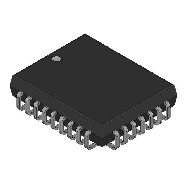
Available in 28-Pin Plastic DIP (NP), Plastic
Small-Outline (DV), and 32-Pin Plastic
J-Leaded Chip-Carrier (RJ) Packages
W
D8
D3
D2
D1
D0
XI
FF
Q0
Q1
Q2
Q3
Q8
GND
1
28
2
27
3
26
4
25
5
24
6
23
7
22
8
21
9
20
10
19
11
18
12
17
13
16
14
15
VCC
D4
D5
D6
D7
FL /RT
RS
EF
XO/HF
Q7
Q6
Q5
Q4
R
RJ PACKAGE
(TOP VIEW)
D3
D8
W
NC
VCC
D4
D5
description
These devices are constructed with dual-port
SRAM and have internal write and read address
counters to provide data throughput on a first-in,
first-out (FIFO) basis. Write and read operations
are independent and can be asynchronous or
coincident. Empty and full status flags prevent
underflow and overflow of memory, and
depth-expansion logic allows combining the
storage cells of two or more devices into one
FIFO. Word-width expansion is also possible.
4
D2
D1
D0
XI
FF
Q0
Q1
NC
Q2
3 2 1 32 31 30
29
6
28
7
27
8
26
9
25
10
24
11
23
12
22
13
21
14 15 16 17 18 19 20
Q3
Q8
Data is loaded into memory by the write-enable
(W) input and unloaded by the read-enable (R)
input. Read and write cycle times of 25 ns
(40 MHz) are possible with data access times of
15 ns.
5
D6
D7
NC
FL /RT
RS
EF
XO/HF
Q7
Q6
GND
NC
R
Q4
Q5
D
DV OR NP PACKAGE
(TOP VIEW)
NC − No internal connection
These devices are particularly suited for providing a data channel between two buses operating at
asynchronous rates. Applications include use as rate buffers from analog-to-digital converters in
data-acquisition systems, temporary storage elements between buses and magnetic or optical memories, and
queues for communication systems. A 9-bit-wide data path is provided for the transmission of byte data plus
a parity bit or packet-framing information. The read pointer can be reset independently of the write pointer for
retransmitting previously read data when a device is not used in depth expansion.
The SN74ACT7203L, SN74ACT7204L, SN74ACT7205L, and SN74ACT7206L are characterized for operation
from 0°C to 70°C.
Please be aware that an important notice concerning availability, standard warranty, and use in critical applications of
Texas Instruments semiconductor products and disclaimers thereto appears at the end of this data sheet.
Copyright 1995, Texas Instruments Incorporated
���������� ���� ��!"#$%&�"� �' ()##*�& %' "! +),-�(%&�"� .%&*/
�#".)(&' ("�!"#$ &" '+*(�!�(%&�"�' +*# &0* &*#$' "! �*1%' ��'&#)$*�&'
'&%�.%#. 2%##%�&3/ �#".)(&�"� +#"(*''��4 ."*' �"& �*(*''%#�-3 ��(-).*
&*'&��4 "! %-- +%#%$*&*#'/
•
POST OFFICE BOX 655303 DALLAS, TEXAS 75265
POST OFFICE BOX 1443 HOUSTON, TEXAS 77251−1443
•
1
����������
�� ��������� ��� ���������
�� ��������� ��
� �� × �� � �� × �� ���� × �� ��
�� × �
������������ ��������� ��������� ��������
SCAS226A − FEBRUARY 1993 − REVISED SEPTEMBER 1995
SN74ACT7203L logic symbol†
FIFO 2048 × 9
Φ
SN74ACT7203L
22
RS
1
W
2,4 CT = 0 (RST)
8
2(CT = 2047) G6
4(CT = 2047) G6
(CT = 2048) G6
6 (WR PNTR)
6 C1
G2
XI
FL /RT
7
23
(EXPAND)
(CT = 0) G5
R
21
EF
(1ST LOAD)
2,4 (REXMIT)
15
FF
(EXPAND)
CT > 1024
5 (RD PNTR)
20
XO/HF
5EN3
G4
(CT = WR PNTR − RD PNTR)
D0
D1
D2
D3
D4
D5
D6
D7
D8
6
1D
3
5
10
4
11
3
12
27
16
26
17
25
18
24
19
2
13
† This symbol is in accordance with ANSI/IEEE Std 91-1984 and IEC Publication 617-12.
Pin numbers shown are for the DV and NP packages.
2
9
•
POST OFFICE BOX 655303 DALLAS, TEXAS 75265
POST OFFICE BOX 1443 HOUSTON, TEXAS 77251−1443
•
Q0
Q1
Q2
Q3
Q4
Q5
Q6
Q7
Q8
����������
�� ��������� ��� ���������
�� ��������� ��
� �� × �� � �� × �� ���� × �� ��
�� × �
������������ ��������� ��������� ��������
SCAS226A − FEBRUARY 1993 − REVISED SEPTEMBER 1995
SN74ACT7204L logic symbol†
FIFO 4096 × 9
Φ
SN74ACT7204L
22
RS
1
W
2,4 CT = 0 (RST)
8
2(CT = 4095) G6
4(CT = 4095) G6
(CT = 4096) G6
6 (WR PNTR)
6 C1
G2
XI
FL /RT
7
23
(EXPAND)
(CT = 0) G5
R
21
EF
(1ST LOAD)
2,4 (REXMIT)
15
FF
(EXPAND)
CT > 2048
5 (RD PNTR)
20
XO/HF
5EN3
G4
(CT = WR PNTR − RD PNTR)
D0
D1
D2
D3
D4
D5
D6
D7
D8
6
1D
3
9
5
10
4
11
3
12
27
16
26
17
25
18
24
19
2
13
Q0
Q1
Q2
Q3
Q4
Q5
Q6
Q7
Q8
† This symbol is in accordance with ANSI/IEEE Std 91-1984 and IEC Publication 617-12.
Pin numbers shown are for the DV and NP packages.
•
POST OFFICE BOX 655303 DALLAS, TEXAS 75265
POST OFFICE BOX 1443 HOUSTON, TEXAS 77251−1443
•
3
����������
�� ��������� ��� ���������
�� ��������� ��
� �� × �� � �� × �� ���� × �� ��
�� × �
������������ ��������� ��������� ��������
SCAS226A − FEBRUARY 1993 − REVISED SEPTEMBER 1995
SN74ACT7205L logic symbol†
FIFO 8192 × 9
Φ
SN74ACT7205L
22
RS
1
W
2,4 CT = 0 (RST)
8
2(CT = 8191) G6
4(CT = 8191) G6
6 (WR PNTR)
6 C1
(CT = 8192) G6
G2
XI
FL /RT
7
23
(EXPAND)
(CT = 0) G5
R
21
EF
(1ST LOAD)
2,4 (REXMIT)
15
FF
(EXPAND)
20
XO/HF
CT > 4096
5 (RD PNTR)
5EN3
G4
(CT = WR PNTR − RD PNTR)
D0
D1
D2
D3
D4
D5
D6
D7
D8
6
1D
3
5
10
4
11
3
12
27
16
26
17
25
18
24
19
2
13
† This symbol is in accordance with ANSI/IEEE Std 91-1984 and IEC Publication 617-12.
Pin numbers shown are for the DV and NP packages.
4
9
•
POST OFFICE BOX 655303 DALLAS, TEXAS 75265
POST OFFICE BOX 1443 HOUSTON, TEXAS 77251−1443
•
Q0
Q1
Q2
Q3
Q4
Q5
Q6
Q7
Q8
����������
�� ��������� ��� ���������
�� ��������� ��
� �� × �� � �� × �� ���� × �� ��
�� × �
������������ ��������� ��������� ��������
SCAS226A − FEBRUARY 1993 − REVISED SEPTEMBER 1995
SN74ACT7206L logic symbol†
FIFO 16384 × 9
Φ
SN74ACT7206L
22
RS
1
W
2,4 CT = 0 (RST)
8
2(CT = 16383) G6
4(CT = 16383) G6
6 (WR PNTR)
6 C1
(CT = 16384) G6
G2
XI
FL /RT
7
23
(EXPAND)
(CT = 0) G5
R
21
EF
(1ST LOAD)
2,4 (REXMIT)
15
FF
(EXPAND)
20
XO/HF
CT > 8192
5 (RD PNTR)
5EN3
G4
(CT = WR PNTR − RD PNTR)
D0
D1
D2
D3
D4
D5
D6
D7
D8
6
1D
3
9
5
10
4
11
3
12
27
16
26
17
25
18
24
19
2
13
Q0
Q1
Q2
Q3
Q4
Q5
Q6
Q7
Q8
† This symbol is in accordance with ANSI/IEEE Std 91-1984 and IEC Publication 617-12.
Pin numbers shown are for the DV and NP packages.
•
POST OFFICE BOX 655303 DALLAS, TEXAS 75265
POST OFFICE BOX 1443 HOUSTON, TEXAS 77251−1443
•
5
����������
�� ��������� ��� ���������
�� ��������� ��
� �� × �� � �� × �� ���� × �� ��
�� × �
������������ ��������� ��������� ��������
SCAS226A − FEBRUARY 1993 − REVISED SEPTEMBER 1995
functional block diagram
9
D0 −D8
Location 1
Location 2
Write
Control
W
2048 × 9 or
4096 × 9 or
8192 × 9 or
16384 × 9
RAM†
Write
Pointer
Read
Pointer
•
9
•
RS
FL /RT
Q0 −Q8
Reset
Logic
StatusFlag
Logic
FF
EF
Read
Control
R
Expansion
Logic
XI
XO/HF
† 2048 × 9 for SN74ACT7203L; 4096 × 9 for SN74ACT7204L; 8192 × 9 for SN74ACT7205L; 16384 × 9 for SN74ACT7206L
RESET AND RETRANSMIT FUNCTION TABLE
(single-device depth; single-or multiple-device width)
INPUTS
INTERNAL TO DEVICE
OUTPUTS
FUNCTION
RS
FL/RT
XI
READ POINTER
WRITE POINTER
EF
FF
XO/HF
L
X
L
Location zero
Location zero
L
H
H
Reset device
H
L
L
Location zero
Unchanged
X
X
X
Retransmit
H
H
L
Increment if EF high
Increment if FF high
X
X
X
Read/write
RESET AND FIRST- LOAD FUNCTION TABLE
(multiple-device depth; single-or multiple-device width)
INPUTS
RS
FL/RT
INTERNAL TO DEVICE
L
L
XI
‡
L
H
‡
H
X
‡
OUTPUTS
WRITE POINTER
EF
FF
Location zero
Location zero
L
H
Reset first device
Location zero
Location zero
L
H
Reset all other devices
X
Read/write
X
X
X
‡ XI is connected to XO/HF of the previous device in the daisy chain (see Figure 15).
6
FUNCTION
READ POINTER
•
POST OFFICE BOX 655303 DALLAS, TEXAS 75265
POST OFFICE BOX 1443 HOUSTON, TEXAS 77251−1443
•
����������
�� ��������� ��� ���������
�� ��������� ��
� �� × �� � �� × �� ���� × �� ��
�� × �
������������ ��������� ��������� ��������
SCAS226A − FEBRUARY 1993 − REVISED SEPTEMBER 1995
Terminal Functions
TERMINAL
NAME
I/O
D0 −D8
I
Data inputs
EF
O
Empty-flag output. EF is low when the read pointer is equal to the write pointer, inhibiting any operation initiated by a read
cycle. When the FIFO is empty, a data word can be read automatically at Q0 −Q8 by holding R low when loading the data
word with a low-level pulse on W.
O
Full-flag output. FF is low when the write pointer is one location less than the read pointer, indicating that the device is
full and inhibiting any operation initiated by a write cycle. FF goes low when the number of writes after reset exceeds the
number of reads by 2048 for the SN74ACT7203L, 4096 for the SN74ACT7204L, 8192 for the SN74ACT7205L, and
16384 for the SN74ACT7206L. When the FIFO is full, a data word can be written automatically into memory by holding
W low while reading out another data word with a low-level pulse on R.
FF
DESCRIPTION
First-load/retransmit input. FL/RT performs two separate functions. When cascading two or more devices for word-depth
expansion, FL /RT is tied to ground on the first device in the daisy chain to indicate that it is the first device loaded and
unloaded; it is tied high on all other devices in the depth-expansion chain.
FL /RT
I
GND
Q0 −Q8
A device is not used in depth expansion when its expansion-in (XI) input is tied to ground. In that case, FL/RT acts as
a retransmit enable. A retransmit operation is initiated when FL /RT is pulsed low. This sets the internal read pointer to
the first location and does not affect the write pointer. R and W must be at a high logic level during the low-level FL /RT
retransmit pulse. Retransmit should be used only when less than 2048/4096 writes are performed between resets;
otherwise, an attempt to retransmit can cause the loss of unread data. The retransmit function can affect XO/HF
depending on the relative locations of the read and write pointers.
Ground
O
Data outputs. Q0 −Q8 are in the high-impedance state when R is high or the FIFO is empty.
R
I
Read-enable input. A read cycle begins on the falling edge of R if EF is high. This activates Q0 −Q8 and shifts the next
data value to this bus. The data outputs return to the high-impedance state as R goes high. As the last stored word is
read by the falling edge of R, EF transitions low but Q0 −Q8 remain active until R returns high. When the FIFO is empty,
the internal read pointer is unchanged by a pulse on R.
RS
I
Reset input. A reset is performed by taking RS low. This initializes the internal read and write pointers to the first location
and sets EF low, FF high, and HF high. Both R and W must be held high for a reset during the window shown in Figure 7.
A reset is required after power up before a write operation can take place.
VCC
Supply voltage
W
I
Write-enable input. A write cycle begins on the falling edge of W if FF is high. The value on D0 −D8 is stored in memory
as W returns high. When the FIFO is full, FF is low inhibiting W from performing any operation on the device.
XI
I
Expansion-in input. XI performs two functions. XI is tied to ground to indicate that the device is not used in depth
expansion. When the device is used in depth expansion, XI is connected to the expansion-out (XO) output of the previous
device in the depth-expansion chain.
XO/HF
O
Expansion-out/half-full-flag output. XO/HF performs two functions. When the device is not used in depth expansion (i.e.,
when XI is tied to ground), XO/HF indicates when half the memory locations are filled. After half of the memory is filled,
the falling edge on W for the next write operation drives XO/HF low. XO/HF remains low until a rising edge of R reduces
the number of words stored to exactly half of the total memory.
When the device is used in depth expansion, XO/HF is connected to XI of the next device in the daisy chain. XO/HF drives
the daisy chain by sending a pulse to the next device when the previous device reaches the last memory location.
•
POST OFFICE BOX 655303 DALLAS, TEXAS 75265
POST OFFICE BOX 1443 HOUSTON, TEXAS 77251−1443
•
7
����������
�� ��������� ��� ���������
�� ��������� ��
� �� × �� � �� × �� ���� × �� ��
�� × �
������������ ��������� ��������� ��������
SCAS226A − FEBRUARY 1993 − REVISED SEPTEMBER 1995
absolute maximum ratings over operating free-air temperature range (unless otherwise noted)†
Supply voltage range, VCC (see Note 1) . . . . . . . . . . . . . . . . . . . . . . . . . . . . . . . . . . . . . . . . . . . . . . −0.5 V to 7 V
Input voltage range (any input), VI . . . . . . . . . . . . . . . . . . . . . . . . . . . . . . . . . . . . . . . . . . . . . . . . . . . . −0.5 V to 7 V
Continuous output current, IO . . . . . . . . . . . . . . . . . . . . . . . . . . . . . . . . . . . . . . . . . . . . . . . . . . . . . . . . . . . . . . 50 mA
Voltage applied to a disabled 3-state output . . . . . . . . . . . . . . . . . . . . . . . . . . . . . . . . . . . . . . . . . . . . . . . . . . 5.5 V
Operating free-air temperature range, TA . . . . . . . . . . . . . . . . . . . . . . . . . . . . . . . . . . . . . . . . . . . . . . 0°C to 70°C
Storage temperature range, Tstg . . . . . . . . . . . . . . . . . . . . . . . . . . . . . . . . . . . . . . . . . . . . . . . . . . −55°C to 125°C
† Stresses beyond those listed under “absolute maximum ratings” may cause permanent damage to the device. These are stress ratings only, and
functional operation of the device at these or any other conditions beyond those indicated under “recommended operating conditions” is not
implied. Exposure to absolute-maximum-rated conditions for extended periods may affect device reliability.
NOTE 1: All voltage values are with respect to GND.
recommended operating conditions
MIN
NOM
MAX
4.5
5
5.5
UNIT
VCC
Supply voltage
VIH
High-level input voltage
VIL
IOH
Low-level input voltage
0.8
V
High-level output current
−2
mA
IOL
TA
Low-level output current
8
mA
70
°C
XI
Other inputs
Operating free-air temperature
2.6
V
V
2
0
electrical characteristics over recommended operating free-air temperature range, VCC = 5.5 V
(unless otherwise noted)
PARAMETER
TEST CONDITIONS
VOH
VOL
VCC = 4.5 V,
VCC = 4.5 V,
IOH = − 2 mA
IOL = 8 mA
IOZH
IOZL
VO = VCC ,
VO = 0.4 V,
II
ICC1‡
VI = 0 to 5.5 V
fclock = 20 MHz
ICC2‡
ICC3‡
R, W, RS, and FL/RT at VIH
Ci§
Co§
VI = VCC − 0.2 V
VI = 0,
MIN
MAX
2.4
UNIT
V
0.4
V
R ≥ VIH
±10
µA
R ≥ VIH
±10
µA
−1
TA = 25°C,
TA = 25°C,
f = 1 MHz
1
µA
120
mA
12
mA
2
mA
10
pF
VO = 0,
f = 1 MHz
10
pF
‡ ICC1 = supply current; ICC2 = standby current; ICC3 = power-down current. ICC measurements are made with outputs open (only capacitive
loading).
§ This parameter is sampled and not 100% tested.
8
•
POST OFFICE BOX 655303 DALLAS, TEXAS 75265
POST OFFICE BOX 1443 HOUSTON, TEXAS 77251−1443
•
����������
�� ��������� ��� ���������
�� ��������� ��
� �� × �� � �� × �� ���� × �� ��
�� × �
������������ ��������� ��������� ��������
SCAS226A − FEBRUARY 1993 − REVISED SEPTEMBER 1995
timing requirements over recommended ranges of supply voltage and operating free-air
temperature (unless otherwise noted)
′ACT7203L-15
′ACT7204L-15
′ACT7205L-15
′ACT7206L-15
FIGURE
MIN
′ACT7203L-25
′ACT7204L-25
′ACT7205L-25
′ACT7206L-25
MAX
MIN
40
MAX
′ACT7203L-50
′ACT7204L-50
′ACT7205L-50
′ACT7206L-50
MIN
MAX
fclock
tc(R)
Clock frequency, R or W
Cycle time, read
1(a)
25
35
65
ns
tc(W)
tc(RS)
Cycle time, write
1(b)
25
35
65
ns
Cycle time, reset
7
25
35
65
ns
tc(RT)
tw(RL)
Cycle time, retransmit
4
25
35
65
ns
Pulse duration, R low
1(a)
15
25
50
ns
tw(WL)
tw(RH)
Pulse duration, W low
1(b)
15
25
50
ns
Pulse duration, R high
1(a)
10
10
15
ns
tw(WH)
tw(RT)
Pulse duration, W high
1(b)
10
10
15
ns
Pulse duration, FL/RT low
4
15
25
50
ns
tw(RS)
tw(XIL)
Pulse duration, RS low
7
15
25
50
ns
Pulse duration, XI low
10
15
25
50
ns
tw(XIH)
tsu(D)
Pulse duration, XI high
10
10
10
10
ns
1(b), 6
11
15
30
ns
tsu(RT)
tsu(RS)
Setup time, R and W high before FL /RT↑†
Setup time, R and W high before RS↑†
4
15
25
50
ns
7
15
25
50
ns
tsu(XI-R)
tsu(XI-W)
Setup time, XI low before R↓
10
10
10
15
ns
Setup time, XI low before W↓
10
10
10
15
ns
th(D)
th(E-R)
Hold time, data after W↑
1(b), 6
0
0
5
ns
Hold time, R low after EF↑
5, 11
15
25
50
ns
th(F-W)
th(RT)
Hold time, W low after FF↑
6, 12
15
25
50
ns
4
10
10
15
ns
7
10
10
15
ns
Setup time, data before W↑
Hold time, R and W high after FL /RT↑
th(RS)
Hold time, R and W high after RS↑
† These values are characterized but not currently tested.
•
POST OFFICE BOX 655303 DALLAS, TEXAS 75265
POST OFFICE BOX 1443 HOUSTON, TEXAS 77251−1443
•
28.5
UNIT
15
MHz
9
����������
�� ��������� ��� ���������
�� ��������� ��
� �� × �� � �� × �� ���� × �� ��
�� × �
������������ ��������� ��������� ��������
SCAS226A − FEBRUARY 1993 − REVISED SEPTEMBER 1995
switching characteristics over recommended ranges of supply voltage and operating free-air
temperature (see Figure 13)
PARAMETER
′ACT7203L-15
′ACT7204L-15
′ACT7205L-15
′ACT7206L-15
FIGURE
MIN
1(a), 3, 5
MAX
′ACT7203L-25
′ACT7204L-25
′ACT7205L-25
′ACT7206L-25
MIN
15
MAX
′ACT7203L-50
′ACT7204L-50
′ACT7205L-50
′ACT7206L-50
MIN
MAX
ta
Access time, R↓ or EF↑ to data out valid
tv(RH)
Valid time, data out valid after R↑
1(a)
5
5
5
ns
ten(R-QX)
Enable time, R↓ to Q outputs at
low impedance†
1(a)
5
5
10
ns
ten(W-QX)
Enable time, W↑ to Q outputs at
low impedance†‡
5
5
5
15
ns
tdis(R)
Disable time, R↑ to Q outputs at
high impedance†
1(a)
15
18
30
ns
tw(FH)
Pulse duration, FF high in
automatic-write mode
6
15
25
45
ns
tw(EH)
Pulse duration, EF high in
automatic-read mode
5
15
25
45
ns
tpd(W-F)
Propagation delay time, W↓ to FF low
2
15
25
45
ns
tpd(R-F)
Propagation delay time, R↑ to FF high
2, 6, 12
15
25
45
ns
tpd(RS-F)
Propagation delay time, RS↓ to FF high
7
25
35
65
ns
tpd(RS-HF)
Propagation delay time, RS↓ to XO/HF
high
7
25
35
65
ns
tpd(W-E)
Propagation delay time, W↑ to EF high
3, 5, 11
15
25
45
ns
tpd(R-E)
Propagation delay time, R↓ to EF low
3
15
25
45
ns
tpd(RS-E)
Propagation delay time, RS↓ to EF low
7
25
35
65
ns
tpd(W-HF)
Propagation delay time, W↓ to XO/HF
low
8
25
35
65
ns
tpd(R-HF)
Propagation delay time, R↑ to XO/HF
high
8
25
35
65
ns
tpd(R-XOL)
Propagation delay time, R↓ to XO/HF
low
9
15
25
50
ns
tpd(W-XOL)
Propagation delay time, W↓ to XO/HF
low
9
15
25
50
ns
tpd(R-XOH)
Propagation delay time, R↑ to XO/HF
high
9
15
25
50
ns
tpd(W-XOH)
Propagation delay time, W↑ to XO/HF
high
9
15
25
50
ns
tpd(RT-FL)
Propagation delay time,
FL/RT↓ to HF, EF, FF valid
4
25
35
65
ns
† These values are characterized but not currently tested.
‡ Only applies when data is automatically read
10
•
POST OFFICE BOX 655303 DALLAS, TEXAS 75265
POST OFFICE BOX 1443 HOUSTON, TEXAS 77251−1443
•
25
UNIT
50
ns
����������
�� ��������� ��� ���������
�� ��������� ��
� �� × �� � �� × �� ���� × �� ��
�� × �
������������ ��������� ��������� ��������
SCAS226A − FEBRUARY 1993 − REVISED SEPTEMBER 1995
PARAMETER MEASUREMENT INFORMATION
tc(R)
tw(RL)
tw(RH)
ta
ta
R
ten(R-QX)
Q0 − Q8
tw(RH)
ÎÎÎ
ÎÎÎ
ÎÎÎÎ
ÎÎÎÎ
Valid
tdis(R)
Valid
ÎÎÎ
ÎÎÎ
(a) READ
tc(W)
tw(WH)
tw(WL)
W
tsu(D)
D0 − D8
th(D)
Valid
Valid
(b) WRITE
Figure 1. Asynchronous Waveforms
Ignored
Write
Last Write
First Read
Additional Reads
R
W
tpd(W-F)
tpd(R-F)
FF
Figure 2. Full-Flag Waveforms
•
POST OFFICE BOX 655303 DALLAS, TEXAS 75265
POST OFFICE BOX 1443 HOUSTON, TEXAS 77251−1443
•
11
����������
�� ��������� ��� ���������
�� ��������� ��
� �� × �� � �� × �� ���� × �� ��
�� × �
������������ ��������� ��������� ��������
SCAS226A − FEBRUARY 1993 − REVISED SEPTEMBER 1995
PARAMETER MEASUREMENT INFORMATION
Ignored
Read
Last Read
First Write
Additional Writes
W
R
tpd(W-E)
tpd(R-E)
EF
ÎÎ ÎÎÎ
ÎÎ ÎÎÎ
ÎÎ ÎÎÎ
ta
D0 − D8
Valid
Figure 3. Empty-Flag Waveforms
tc(RT)
tw(RT)
FL /RT
ÏÏÏÏÏÏÏÏ
ÏÏÏÏÏÏÏÏ
ÏÏÏÏÏÏÏÏ
ÎÎÎÎÎÎÎÎÎÎÎÎÎÎÎÎ
ÎÎÎÎÎÎÎÎÎÎÎÎÎÎÎÎ
W, R
tsu(RT)
th(RT)
XO / HF, EF, FF
tpd(RT-FL)
NOTE A: The EF, FF, and XO/HF status flags are valid after completion of the retransmit cycle.
Figure 4. Retransmit Waveforms
12
•
POST OFFICE BOX 655303 DALLAS, TEXAS 75265
POST OFFICE BOX 1443 HOUSTON, TEXAS 77251−1443
•
Valid Flag
����������
�� ��������� ��� ���������
�� ��������� ��
� �� × �� � �� × �� ���� × �� ��
�� × �
������������ ��������� ��������� ��������
SCAS226A − FEBRUARY 1993 − REVISED SEPTEMBER 1995
PARAMETER MEASUREMENT INFORMATION
W
th(E-R)
R
EF
tw(EH)
tpd(W-E)
ten(W-QX)
Q0 − Q8
ÎÎÎÎÎÎ
ÎÎÎÎÎÎ
ta
Valid
Figure 5. Automatic-Read Waveforms
R
th(F-W)
W
tpd(R-F)
FF
tw(FH)
th(D)
D0 − D8
Valid
tsu(D)
Figure 6. Automatic-Write Waveforms
•
POST OFFICE BOX 655303 DALLAS, TEXAS 75265
POST OFFICE BOX 1443 HOUSTON, TEXAS 77251−1443
•
13
����������
�� ��������� ��� ���������
�� ��������� ��
� �� × �� � �� × �� ���� × �� ��
�� × �
������������ ��������� ��������� ��������
SCAS226A − FEBRUARY 1993 − REVISED SEPTEMBER 1995
PARAMETER MEASUREMENT INFORMATION
tc(RS)
tw(RS)
RS
ÏÏÏÏÏÏÏÏÏÏÏÏÏÏÏÏ
ÏÏÏÏÏÏÏÏÏÏÏÏÏÏÏÏ
ÏÏÏÏÏÏÏÏÏÏÏÏÏÏÏÏ
ÏÏÏÏÏÏÏÏÏÏÏÏÏÏÏÏ
ÌÌÌÌÌÌÌÌÌÌÌÌÌ
ÌÌÌÌÌÌÌÌÌÌÌÌÌ
ÏÏÏÏÏÏÏÏÏÏÏÏÏ
ÏÏÏÏÏÏÏÏÏÏÏÏÏ
W
R
tsu(RS)
th(RS)
EF
tpd(RS-E)
XO/HF, FF
tpd(RS-HF)
tpd(RS-F)
Figure 7. Master-Reset Waveforms
Half Full or Less
More Than Half Full
Half Full or Less
W
tpd(R-HF)
R
tpd(W-HF)
XO/HF
Figure 8. Half-Full Flag Waveforms
14
•
POST OFFICE BOX 655303 DALLAS, TEXAS 75265
POST OFFICE BOX 1443 HOUSTON, TEXAS 77251−1443
•
����������
�� ��������� ��� ���������
�� ��������� ��
� �� × �� � �� × �� ���� × �� ��
�� × �
������������ ��������� ��������� ��������
SCAS226A − FEBRUARY 1993 − REVISED SEPTEMBER 1995
PARAMETER MEASUREMENT INFORMATION
W
R
Write to Last
Physical Location
Read From Last
Physical Location
tpd(W-XOH)
tpd(W-XOL)
tpd(R-XOL)
tpd(R-XOH)
XO/HF
Figure 9. Expansion-Out Waveforms
tw(XIL)
tw(XIH)
XI
tsu(XI-W)
W
Write to First
Physical Location
tsu(XI-R)
Read From First
Physical Location
R
Figure 10. Expansion-In Waveforms
W
tpd(W-E)
EF
ÌÌÌÌÌÌÌÌÌÌÌÌÌÌÌÌÌÌÌÌÌ
ÌÌÌÌÌÌÌÌÌÌÌÌÌÌÌÌÌÌÌÌÌ
ÌÌÌÌÌÌÌÌÌÌÌÌÌÌÌÌÌÌÌÌÌ
th(E-R)
R
Figure 11. Minimum Timing for an Empty-Flag Coincident-Read Pulse
•
POST OFFICE BOX 655303 DALLAS, TEXAS 75265
POST OFFICE BOX 1443 HOUSTON, TEXAS 77251−1443
•
15
����������
�� ��������� ��� ���������
�� ��������� ��
� �� × �� � �� × �� ���� × �� ��
�� × �
������������ ��������� ��������� ��������
SCAS226A − FEBRUARY 1993 − REVISED SEPTEMBER 1995
PARAMETER MEASUREMENT INFORMATION
R
tpd(R-F)
FF
W
ÌÌÌÌÌÌÌÌÌÌÌÌÌÌÌÌÌÌÌÌÌ
ÌÌÌÌÌÌÌÌÌÌÌÌÌÌÌÌÌÌÌÌÌ
ÌÌÌÌÌÌÌÌÌÌÌÌÌÌÌÌÌÌÌÌÌ
Figure 12. Minimum Timing for a Full-Flag Coincident-Write Pulse
16
•
POST OFFICE BOX 655303 DALLAS, TEXAS 75265
POST OFFICE BOX 1443 HOUSTON, TEXAS 77251−1443
•
th(F-W)
����������
�� ��������� ��� ���������
�� ��������� ��
� �� × �� � �� × �� ���� × �� ��
�� × �
������������ ��������� ��������� ��������
SCAS226A − FEBRUARY 1993 − REVISED SEPTEMBER 1995
PARAMETER MEASUREMENT INFORMATION
5V
1100 Ω
From Output
Under Test
680 Ω
30 pF
(see Note A)
LOAD CIRCUIT
3V
Timing
Input
1.5 V
GND
tw
3V
1.5 V
3V
1.5 V
Low-Level
Input
GND
1.5 V
1.5 V
GND
VOLTAGE WAVEFORMS
SETUP AND HOLD TIMES
Output
Enable
1.5 V
GND
th
tsu
Data,
Enable
Input
3V
High-Level
Input
1.5 V
VOLTAGE WAVEFORMS
PULSE DURATIONS
3V
1.5 V
1.5 V
GND
tPLZ
tPZL
Low-Level
Output
≈3V
3V
1.5 V
VOL
1.5 V
GND
tPZH
tpd
tpd
VOH
High-Level
Output
1.5 V
Input
1.5 V
VOH
In-Phase
Output
≈0V
1.5 V
1.5 V
VOL
tPHZ
VOLTAGE WAVEFORMS
PROPAGATION DELAY TIMES
VOLTAGE WAVEFORMS
ENABLE AND DISABLE TIMES
NOTE A: Includes probe and jig capacitance
Figure 13. Load Circuit and Voltage Waveforms
•
POST OFFICE BOX 655303 DALLAS, TEXAS 75265
POST OFFICE BOX 1443 HOUSTON, TEXAS 77251−1443
•
17
����������
�� ��������� ��� ���������
�� ��������� ��
� �� × �� � �� × �� ���� × �� ��
�� × �
������������ ��������� ��������� ��������
SCAS226A − FEBRUARY 1993 − REVISED SEPTEMBER 1995
APPLICATION INFORMATION
Combining two or more devices to create one FIFO with a greater number of memory bits is accomplished in two
different ways. Width expansion increases the number of bits in each word by connecting FIFOs with the same depth
in parallel. Depth expansion uses the built-in expansion logic to daisy-chain two or more devices for applications
requiring more than 2048, 4096, 8192, or 16384 words of storage. Width expansion and depth expansion can be used
together.
width expansion
Word-width expansion is achieved by connecting the corresponding input control to multiple devices with the
same depth. Status flags (EF, FF, and HF) can be monitored from any one device. Figure 14 shows two FIFOs
in a width-expansion configuration. Both devices have their expansion-in (XI) inputs tied to ground. This
disables the depth-expansion function of the device, allowing the first-load/retransmit (FL/RT) input to function
as a retransmit (RT) input and the expansion-out/half-full (XO/HF) output to function as a half-full (HF) flag.
depth expansion
The SN74ACT7203L / 7204L/7205L/7206L are easily expanded in depth. Figure 15 shows the connections
used to depth expand three SN74ACT7203L / 7204L/7205L/7206L devices. Any depth can be attained by
adding additional devices to the chain. The SN74ACT7203L/ 7204L/7205L/7206L operate in depth expansion
under the following conditions:
D
D
D
D
The first device in the chain is designated by connecting FL to ground.
All other devices have their FL inputs at a high logic level.
XO of each device must be connected to XI of the next device.
External logic is needed to generate a composite FF and EF. All FF outputs must be ORed together,
and all EF outputs must be ORed together.
D RT and HF functions are not available in the depth-expanded configuration.
combined depth and width expansion
Both expansion techniques can be used together to increase depth and width. This is done by creating
depth-expanded units and then connecting them in a width-expanded configuration (see Figure 16).
18
•
POST OFFICE BOX 655303 DALLAS, TEXAS 75265
POST OFFICE BOX 1443 HOUSTON, TEXAS 77251−1443
•
����������
�� ��������� ��� ���������
�� ��������� ��
� �� × �� � �� × �� ���� × �� ��
�� × �
������������ ��������� ��������� ��������
SCAS226A − FEBRUARY 1993 − REVISED SEPTEMBER 1995
APPLICATION INFORMATION
SN74ACT7203L / 7204L/7205L/7206L
18
D0 −D18
D0 − D8
Q0 − Q8
Q0 −Q8
D0 −D8
9
9
18
Q0 −Q18
W
W
R
R
EF
EF
RT
FL /RT
FF
FF
RS
RS
XO/HF
HF
XI
SN74ACT7203L / 7204L/7205L/7206L
D9 − D18
Q9 − Q18
Q0 −Q8
D0 −D8
9
9
W
R
EF
EF
FL /RT
FF
FF
XO/HF
HF
RS
XI
Figure 14. Word-Width Expansion: 2048 / 4096 Words × 18 Bits
•
POST OFFICE BOX 655303 DALLAS, TEXAS 75265
POST OFFICE BOX 1443 HOUSTON, TEXAS 77251−1443
•
19
����������
�� ��������� ��� ���������
�� ��������� ��
� �� × �� � �� × �� ���� × �� ��
�� × �
������������ ��������� ��������� ��������
SCAS226A − FEBRUARY 1993 − REVISED SEPTEMBER 1995
APPLICATION INFORMATION
SN74ACT7203L / 7204L/7205L/7206L
9
9
D0 −D8
9
D0 −D8
W
W
R
R
RS
9
Q0 −Q8
Q0 −Q8
XO/HF
RS
EF
FL /RT
FF
XI
SN74ACT7203L / 7204L/7205L/7206L
9
D0 −D8
Q0 −Q8
9
W
EF
R
VCC
XO/HF
RS
EF
FL /RT
FF
XI
FF
SN74ACT7203L / 7204L/7205L/7206L
9
D0 −D8
Q0 −Q8
9
W
R
XO/HF
RS
EF
FL /RT
FF
XI
Figure 15. Word-Depth Expansion: 6144 / 12288/24576/49152 Words × 9 Bits
20
•
POST OFFICE BOX 655303 DALLAS, TEXAS 75265
POST OFFICE BOX 1443 HOUSTON, TEXAS 77251−1443
•
����������
�� ��������� ��� ���������
�� ��������� ��
� �� × �� � �� × �� ���� × �� ��
�� × �
������������ ��������� ��������� ��������
SCAS226A − FEBRUARY 1993 − REVISED SEPTEMBER 1995
APPLICATION INFORMATION
Q0 −Q17
Q0 −Q26
18
9
9
27
D0 −D26
Q9 −Q17
′ACT7203L
or
′ACT7204L
or
′ACT7205L
or
′ACT7206L
Depth Expansion
Block
′ACT7203L
or
′ACT7204L
or
′ACT7205L
or
′ACT7206L
Depth Expansion
Block
W, R, RS
9
Q0 −Q8
9
D0 −D8
D9 −D17
27
9
Q18 −Q26
′ACT7203L
or
′ACT7204L
or
′ACT7205L
or
′ACT7206L
Depth Expansion
Block
9
D18 −D26
18
D9 −D26
Figure 16. Word-Depth Plus Word-Width Expansion
•
POST OFFICE BOX 655303 DALLAS, TEXAS 75265
POST OFFICE BOX 1443 HOUSTON, TEXAS 77251−1443
•
21
�IMPORTANT NOTICE
Texas Instruments Incorporated and its subsidiaries (TI) reserve the right to make corrections, modifications, enhancements, improvements,
and other changes to its products and services at any time and to discontinue any product or service without notice. Customers should
obtain the latest relevant information before placing orders and should verify that such information is current and complete. All products are
sold subject to TI’s terms and conditions of sale supplied at the time of order acknowledgment.
TI warrants performance of its hardware products to the specifications applicable at the time of sale in accordance with TI’s standard
warranty. Testing and other quality control techniques are used to the extent TI deems necessary to support this warranty. Except where
mandated by government requirements, testing of all parameters of each product is not necessarily performed.
TI assumes no liability for applications assistance or customer product design. Customers are responsible for their products and
applications using TI components. To minimize the risks associated with customer products and applications, customers should provide
adequate design and operating safeguards.
TI does not warrant or represent that any license, either express or implied, is granted under any TI patent right, copyright, mask work right,
or other TI intellectual property right relating to any combination, machine, or process in which TI products or services are used. Information
published by TI regarding third-party products or services does not constitute a license from TI to use such products or services or a
warranty or endorsement thereof. Use of such information may require a license from a third party under the patents or other intellectual
property of the third party, or a license from TI under the patents or other intellectual property of TI.
Reproduction of TI information in TI data books or data sheets is permissible only if reproduction is without alteration and is accompanied
by all associated warranties, conditions, limitations, and notices. Reproduction of this information with alteration is an unfair and deceptive
business practice. TI is not responsible or liable for such altered documentation. Information of third parties may be subject to additional
restrictions.
Resale of TI products or services with statements different from or beyond the parameters stated by TI for that product or service voids all
express and any implied warranties for the associated TI product or service and is an unfair and deceptive business practice. TI is not
responsible or liable for any such statements.
TI products are not authorized for use in safety-critical applications (such as life support) where a failure of the TI product would reasonably
be expected to cause severe personal injury or death, unless officers of the parties have executed an agreement specifically governing
such use. Buyers represent that they have all necessary expertise in the safety and regulatory ramifications of their applications, and
acknowledge and agree that they are solely responsible for all legal, regulatory and safety-related requirements concerning their products
and any use of TI products in such safety-critical applications, notwithstanding any applications-related information or support that may be
provided by TI. Further, Buyers must fully indemnify TI and its representatives against any damages arising out of the use of TI products in
such safety-critical applications.
TI products are neither designed nor intended for use in military/aerospace applications or environments unless the TI products are
specifically designated by TI as military-grade or "enhanced plastic." Only products designated by TI as military-grade meet military
specifications. Buyers acknowledge and agree that any such use of TI products which TI has not designated as military-grade is solely at
the Buyer's risk, and that they are solely responsible for compliance with all legal and regulatory requirements in connection with such use.
TI products are neither designed nor intended for use in automotive applications or environments unless the specific TI products are
designated by TI as compliant with ISO/TS 16949 requirements. Buyers acknowledge and agree that, if they use any non-designated
products in automotive applications, TI will not be responsible for any failure to meet such requirements.
Following are URLs where you can obtain information on other Texas Instruments products and application solutions:
Products
Amplifiers
Data Converters
DSP
Clocks and Timers
Interface
Logic
Power Mgmt
Microcontrollers
RFID
RF/IF and ZigBee® Solutions
amplifier.ti.com
dataconverter.ti.com
dsp.ti.com
www.ti.com/clocks
interface.ti.com
logic.ti.com
power.ti.com
microcontroller.ti.com
www.ti-rfid.com
www.ti.com/lprf
Applications
Audio
Automotive
Broadband
Digital Control
Medical
Military
Optical Networking
Security
Telephony
Video & Imaging
Wireless
www.ti.com/audio
www.ti.com/automotive
www.ti.com/broadband
www.ti.com/digitalcontrol
www.ti.com/medical
www.ti.com/military
www.ti.com/opticalnetwork
www.ti.com/security
www.ti.com/telephony
www.ti.com/video
www.ti.com/wireless
Mailing Address: Texas Instruments, Post Office Box 655303, Dallas, Texas 75265
Copyright © 2008, Texas Instruments Incorporated
�