SN54ACT8990, SN74ACT8990
TEST-BUS CONTROLLERS
IEEE STD 1149.1 (JTAG) TAP MASTERS WITH 16-BIT GENERIC HOST INTERFACES
SCAS190E – JUNE 1990 – REVISED JANUARY 1997
D
D
D
D
D
Members of the Texas Instruments
SCOPE Family of Testability Products
Compatible With the IEEE Standard
1149.1-1990 (JTAG) Test Access Port and
Boundary-Scan Architecture
Control Operation of Up to Six Parallel
Target Scan Paths
Accommodate Pipeline Delay to Target of
Up to 31 Clock Cycles
Scan Data Up to 232 Clock Cycles
D
D
D
D
D
Execute Instructions for Up to 232 Clock
Cycles
Each Device Includes Four Bidirectional
Event Pins for Additional Test Capability
Inputs Are TTL-Voltage Compatible
EPIC (Enhanced-Performance Implanted
CMOS) 1-µm Process
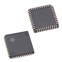
Packaged in 44-Pin Plastic Leaded Chip
Carrier (FN), 68-Pin Ceramic Pin Grid Array
(GB), and 68-Pin Ceramic Quad Flat
Packages (HV)
description
The ’ACT8990 test-bus controllers (TBC) are members of the Texas Instruments SCOPE testability
integrated-circuit family. This family of components supports IEEE Standard 1149.1-1990 (JTAG) boundary
scan to facilitate testing of complex circuit-board assemblies. The ’ACT8990 differ from other SCOPE
integrated circuits. Their function is to control the JTAG serial-test bus rather than being target
boundary -scannable devices.
The required signals of the JTAG serial-test bus – test clock (TCK), test mode select (TMS), test data input (TDI),
and test data output (TDO) can be connected from the TBC to a target device without additional logic. This is
done as a chain of IEEE Standard 1149.1-1990 boundary-scannable components that share the same
serial-test bus. The TBC generates TMS and TDI signals for its target(s), receives TDO signals from its target(s),
and buffers its test clock input (TCKI) to a test clock output (TCKO) for distribution to its target(s). The TMS, TDI,
and TDO signals can be connected to a target directly or via a pipeline, with a retiming delay of up to 31 bits.
Since the TBC can be configured to generate up to six separate TMS signals [TMS (5 – 0)], it can be used to
control up to six target scan paths that are connected in parallel (i.e., sharing common TCK, TDI, and TDO
signals).
While most operations of the TBC are synchronous to TCKI, a test-off (TOFF) input is provided for output control
of the target interface, and a test-reset (TRST) input is provided for hardware/software reset of the TBC. In
addition, four event [EVENT (3 – 0)] I/Os are provided for asynchronous communication to target device(s).
Each event has its own event generation/detection logic, and detected events can be counted by two 16-bit
counters.
The TBC operates under the control of a host microprocessor/microcontroller via the 5-bit address bus
[ADRS (4 – 0)] and the 16-bit read/write data bus [DATA (15 – 0)]. Read (RD) and write (WR) strobes are
implemented such that the critical host-interface timing is independent of the TCKI period. Any one of
24 registers can be addressed for read and/or write operations. In addition to control and status registers, the
TBC contains two command registers, a read buffer, and a write buffer. Status of the TBC is transmitted to the
host via ready (RDY) and interrupt (INT) outputs.
Major commands can be issued by the host to cause the TBC to generate the TMS sequences necessary to
move the target(s) from any stable test-access-port (TAP) controller state to any other stable TAP state, to
execute instructions in the Run-Test/Idle TAP state, or to scan instruction or test data through the target(s). A
32-bit counter can be preset to allow a predetermined number of execution or scan operations.
Serial data that appears at the selected TDI input (TDI1 or TDI0) is transferred into the read buffer, which can
be read by the host to obtain up to 16 bits of the serial-data stream. Serial data that is transmitted from the TDO
output is written by the host to the write buffer.
Please be aware that an important notice concerning availability, standard warranty, and use in critical applications of
Texas Instruments semiconductor products and disclaimers thereto appears at the end of this data sheet.
SCOPE and EPIC are trademarks of Texas Instruments Incorporated.
Copyright 1997, Texas Instruments Incorporated
PRODUCTION DATA information is current as of publication date.
Products conform to specifications per the terms of Texas Instruments
standard warranty. Production processing does not necessarily include
testing of all parameters.
On products compliant to MIL-PRF-38535, all parameters are tested
unless otherwise noted. On all other products, production
processing does not necessarily include testing of all parameters.
POST OFFICE BOX 655303
• DALLAS, TEXAS 75265
1
�SN54ACT8990, SN74ACT8990
TEST-BUS CONTROLLERS
IEEE STD 1149.1 (JTAG) TAP MASTERS WITH 16-BIT GENERIC HOST INTERFACES
SCAS190E – JUNE 1990 – REVISED JANUARY 1997
description (continued)
The SN54ACT8990 is characterized for operation over the full military temperature range of –55°C to 125°C.
The SN74ACT8990 is characterized for operation from 0°C to 70°C.
9 8 7 6 5 4 3 2 1 68 67 66 65 64 63 62 61
60
10
11
59
12
58
13
57
14
56
15
55
16
54
17
53
18
52
19
51
20
50
21
49
22
48
23
47
24
46
25
45
DATA14
NC
DATA15
TOFF
NC
TDI0
TDI1
NC
VCC
44
26
27 28 29 30 31 32 33 34 35 36 37 38 39 40 41 42 43
NC
DATA9
DATA10
NC
DATA11
DATA12
NC
DATA13
NC
DATA0
DATA1
NC
DATA2
DATA3
NC
DATA4
GND
VCC
NC
DATA5
DATA6
NC
DATA7
DATA8
NC
NC – No internal connection
2
TRST
NC
NC
ADRS4
ADRS3
NC
ADRS2
ADRS1
NC
ADRS0
GND
INT
NC
RDY
RD
NC
WR
SN54ACT8990 . . . HV PACKAGE
(TOP VIEW)
POST OFFICE BOX 655303
• DALLAS, TEXAS 75265
NC
TMS5/EVENT3
TMS4/EVENT2
NC
TMS3/EVENT1
TMS2/EVENT0
NC
VCC
GND
TMS1
NC
TMS0
TDO
NC
TCKO
TCKI
NC
�SN54ACT8990, SN74ACT8990
TEST-BUS CONTROLLERS
IEEE STD 1149.1 (JTAG) TAP MASTERS WITH 16-BIT GENERIC HOST INTERFACES
SCAS190E – JUNE 1990 – REVISED JANUARY 1997
ADRS4
ADRS3
ADRS2
ADRS1
ADRS0
GND
INT
RDY
RD
WR
TRST
SN74ACT8990 . . . FN PACKAGE
(TOP VIEW)
7
2 1 44 43 42 41 40
39
8
38
9
37
10
36
11
35
12
34
13
33
14
32
15
31
6 5
4
3
TMS5/EVENT3
TMS4/EVENT2
TMS3/EVENT1
TMS2/EVENT0
VCC
GND
TMS1
TMS0
TDO
TCKO
TCKI
16
VCC
DATA14
DATA15
TOFF
TDI0
TDI1
30
17
29
18 19 20 21 22 23 24 25 26 27 28
DATA9
DATA10
DATA11
DATA12
DATA13
DATA0
DATA1
DATA2
DATA3
DATA4
GND
VCC
DATA5
DATA6
DATA7
DATA8
SN54ACT8990 . . . GB PACKAGE
(TOP VIEW)
1
2
3
4
5
6
7
8
9
10
11
A
B
C
D
E
F
G
H
J
K
L
POST OFFICE BOX 655303
• DALLAS, TEXAS 75265
3
�SN54ACT8990, SN74ACT8990
TEST-BUS CONTROLLERS
IEEE STD 1149.1 (JTAG) TAP MASTERS WITH 16-BIT GENERIC HOST INTERFACES
SCAS190E – JUNE 1990 – REVISED JANUARY 1997
Table 1. Terminal Assignments
TERMINAL
TERMINAL
TERMINAL
TERMINAL
NO.
NAME
NO.
NAME
NO.
NAME
NO.
A2
NC
B10
NC
F11
NC
K6
NAME
NC
A3
ADRS4
B11
NC
G1
DATA5
K7
A4
NC
C1
DATA2
G2
NC
K8
VCC
DATA15
A5
ADRS1
C2
DATA1
G10
NC
K9
TDI0
A6
ADRS0
C3
NC
G11
TMS1
K10
NC
A7
NC
C10
TMS4/EVENT2
H1
NC
K11
TCKI
A8
INT
C11
TMS5/EVENT3
H2
DATA6
L2
DATA9
A9
RD
D1
DATA4
H10
TDO
L3
NC
A10
TRST
D2
DATA3
H11
TMS0
L4
DATA12
B1
DATA0
D10
TMS3/EVENT1
J1
DATA8
L5
DATA13
B2
NC
D11
NC
J2
DATA7
L6
NC
B3
ADRS3
E1
NC
J10
TCKO
L7
DATA14
B4
ADRS2
E2
GND
J11
NC
L8
TOFF
B5
NC
E10
K1
NC
L9
TDI1
B6
NC
E11
VCC
TMS2/EVENT0
K2
NC
L10
NC
B7
GND
F1
K3
DATA10
B8
RDY
F2
VCC
NC
K4
DATA11
B9
WR
F10
GND
K5
NC
NC – No internal connection
functional block diagram
Target
Interface
Host
Interface
Read Data Bus
16
Write Data Bus
16
16
DATA(15 – 0)†
5
ADRS(4 – 0)
TMS(5 – 2)/
EVENT(3 – 0)†
4
Event
Block
RD
Counter Block
WR
RDY
Command Block
TMS(1 – 0)
TDI(1 – 0)†
TDO
2
2
Sequencer
Block
Serial Block
TOFF†
TCKO
TCKI
TRST †
† Inputs have internal pullup resistors.
4
POST OFFICE BOX 655303
• DALLAS, TEXAS 75265
Host
Block
INT
�SN54ACT8990, SN74ACT8990
TEST-BUS CONTROLLERS
IEEE STD 1149.1 (JTAG) TAP MASTERS WITH 16-BIT GENERIC HOST INTERFACES
SCAS190E – JUNE 1990 – REVISED JANUARY 1997
Terminal Functions
TERMINAL NAME
I/O
DESCRIPTION
ADRS4 – ADRS0
I
Address inputs. ADRS4 – ADRS0 form the 5-bit address bus that interfaces the TBC to its host. These inputs
specify the TBC register to be read from or written to.
DATA15 – DATA0
I/O
Data inputs and outputs. DATA15 – DATA0 form the 16-bit bidirectional data bus that interfaces the TBC to its
host. Data is read from or written to the TBC register using this data bus.
GND
INT
Ground
O
NC
Interrupt. INT transmits an interrupt signal to the host. When the TBC requires service from the host, INT is
asserted (low). INT will remain asserted (low) until the host has completed the required service.
No connection
RD
I
Read strobe. RD is the active low output enable for the data bus. RD is used as the strobe for reading data from
the selected TBC register.
RDY
O
Ready. RDY transmits a status signal to the host. When the TBC is ready to accept a read or write operation
from the host, RDY is asserted (low). RDY is not asserted (high) when the TBC is in recovery from a read, write,
command, or reset operation.
TCKI
I
Test clock input. TCKI is the clock input for the TBC. Most operations of the TBC are synchronous to TCKI.
When enabled, all target interface outputs change on the falling edge of TCKI. Sampling of target interface
inputs are configured to occur on either the rising edge or falling edge of TCKI.
TCKO
O
Test clock output. TCKO distributes TCK to the target(s). The TCKO is configured to be disabled, constant zero,
constant one, or to follow TCKI. When TCKO follows TCKI, it is delayed to match the delay of generating the
TDO and TMS signals.
TDI1 – TDI0
I
Test data inputs. The TDI1 – TDI0 serial inputs are used for shifting test data from the target(s). The TDI inputs
can be directly connected to the TDO pin(s) of the target(s).
TDO
O
Test data output. TDO is used for shifting test data into the target(s). TDO can be directly connected to the TDI
terminal(s) of the target(s).
TMS1 – TMS0
O
Test mode select outputs. These parallel outputs transmit TMS signals to the target(s), which direct them
through their TAP controller states. TMS1 – TMS0 can be directly connected to the TMS terminals of the
target(s).
TMS5 – TMS2/
EVENT3 – EVENT0
I/O
Test mode select outputs or event inputs/outputs. These I/Os can be configured for use as either TMS outputs
or event inputs/outputs. As TMS outputs, they function similarly to TMS1 – TMS0 above. As event I/Os, they
can be used to receive/transmit interrupt signals to/from the target(s).
TOFF
I
Test-off input. TOFF is the active low output disable for all outputs and I/Os of the target interface (TCKO, TDO,
TMS, TMS/EVENT).
TRST
I
Test-reset input. TRST is used to initiate hardware and software reset operations of the TBC. Hardware reset
begins when TRST is asserted (low). Software reset begins when TRST is released (high) and proceeds
synchronously to TCKI to completion in a predetermined number of cycles.
WR
I
Write input. WR is the strobe for writing data to a TBC data register. Signals present at the data and address
buses are captured on the rising edge of WR.
VCC
Supply voltage
POST OFFICE BOX 655303
• DALLAS, TEXAS 75265
5
�SN54ACT8990, SN74ACT8990
TEST-BUS CONTROLLERS
IEEE STD 1149.1 (JTAG) TAP MASTERS WITH 16-BIT GENERIC HOST INTERFACES
SCAS190E – JUNE 1990 – REVISED JANUARY 1997
absolute maximum ratings over operating free-air temperature range (unless otherwise noted)†
Supply voltage range, VCC . . . . . . . . . . . . . . . . . . . . . . . . . . . . . . . . . . . . . . . . . . . . . . . . . . . . . . . . . . –0.5 V to 7 V
Input voltage range, VI (see Note 1) . . . . . . . . . . . . . . . . . . . . . . . . . . . . . . . . . . . . . . . . . . . . . . . . . –0.5 V to VCC
Output voltage range, VO (see Note 1) . . . . . . . . . . . . . . . . . . . . . . . . . . . . . . . . . . . . . . . . . . . . . . –0.5 V to VCC
Input clamp current, IIK (VI < 0 or VI > VCC) . . . . . . . . . . . . . . . . . . . . . . . . . . . . . . . . . . . . . . . . . . . . . . . . ±20 mA
Output clamp current, IOK (VO < 0 or VO > VCC) . . . . . . . . . . . . . . . . . . . . . . . . . . . . . . . . . . . . . . . . . . . . ±20 mA
Continuous output current, IO (VO = 0 to VCC) . . . . . . . . . . . . . . . . . . . . . . . . . . . . . . . . . . . . . . . . . . . . . . ±25 mA
Maximum power dissipation at TA = 55°C (in still air) (see Note 2): FN package . . . . . . . . . . . . . . . . . . . 1.5W
Storage temperature range, Tstg . . . . . . . . . . . . . . . . . . . . . . . . . . . . . . . . . . . . . . . . . . . . . . . . . . . –65°C to 150°C
† Stresses beyond those listed under “absolute maximum ratings” may cause permanent damage to the device. These are stress ratings only, and
functional operation of the device at these or any other conditions beyond those indicated under “recommended operating conditions” is not
implied. Exposure to absolute-maximum-rated conditions for extended periods may affect device reliability.
NOTES: 1. The input and output voltage ratings may be exceeded if the input and output clamp-current ratings are observed.
2. The maximum package power dissipation is calculated using a junction temperature of 150°C and a board trace length of 75 mils.
For more information, refer to the Package Thermal Considerations application note in the ABT Advanced BiCMOS Technology Data
Book, literature number SCBD002.
recommended operating conditions
SN54ACT8990
SN74ACT8990
MIN
MAX
MIN
MAX
4.5
5.5
4.5
5.5
UNIT
VCC
VIH
Supply voltage
VIL
VI
Low-level input voltage
Input voltage
0
VO
IOH
Output voltage
0
High-level output current
–8
–8
mA
IOL
TA
Low-level output current
8
8
mA
70
°C
6
High-level input voltage
2
2
0.8
Operating free-air temperature
–55
POST OFFICE BOX 655303
• DALLAS, TEXAS 75265
VCC
VCC
125
0
0
0
V
V
0.8
V
VCC
VCC
V
V
�SN54ACT8990, SN74ACT8990
TEST-BUS CONTROLLERS
IEEE STD 1149.1 (JTAG) TAP MASTERS WITH 16-BIT GENERIC HOST INTERFACES
SCAS190E – JUNE 1990 – REVISED JANUARY 1997
electrical characteristics over recommended operating free-air temperature range (unless
otherwise noted)
PARAMETER
TEST CONDITIONS
ICC
Ci
Cio
Co
SN54ACT8990
MIN
MAX
SN74ACT8990
MIN
MAX
IOH = –20 µA
IOH = – 8 mA
4.4
4.4
4.4
3.7
3.7
3.7
5V
VCC = 5
5.5
IOH = –20 µA
IOH = –8 mA
5.4
5.4
5.4
VCC = 4.5 V
to 5.5 V
IOL = 20 µA
IOL = 8 mA
0.1
0.1
0.1
0.5
0.5
0.5
ADRS, RD,
WR, TCKI
VCC = 5.5 V,
VI = VCC or GND
±1
±1
±1
TDI, TOFF,
TRST
VCC = 5
5.5
5V
VI = VCC
VI = GND
±1
±1
±1
INT, RDY, TCKO,
TDO, TMS
VCC = 5.5 V,
VO = VCC or GND
±10
±10
±10
DATA,,
TMS/EVENT
VCC = 5
5.5
5V
VO = VCC
VO = GND
±10
±10
±10
VCC = 5.5 V,
IO = 0,
VI = VCC or GND
VOL
IOZ‡
TA = 25°C
TYP†
MAX
VCC = 4
4.5
5V
VOH
II
MIN
4.7
–35
–35
4.7
–70
–70
–250
–250
450*
VCC = 5.5 V,
CL = 50 pF
fclock = 30 MHz
VI = VCC or GND
VI = VCC or GND
VI = VCC or GND
–35
–35
UNIT
V
4.7
–250
–250
450
–35
–35
V
A
µA
–250
A
µA
–250
450
µA
100
mA
5*
9*
pF
8*
pF
pF
* On products compliant to MIL-PRF-38535, this parameter does not apply.
† Typical values are at VCC = 5 V.
‡ For I/O ports, the parameter IOZ includes the input leakage.
POST OFFICE BOX 655303
• DALLAS, TEXAS 75265
7
�SN54ACT8990, SN74ACT8990
TEST-BUS CONTROLLERS
IEEE STD 1149.1 (JTAG) TAP MASTERS WITH 16-BIT GENERIC HOST INTERFACES
SCAS190E – JUNE 1990 – REVISED JANUARY 1997
timing requirements over recommended ranges of supply voltage and operating free-air
temperature (see Figure 1)
SN54ACT8990
fclock
Clock frequency
MIN
MAX
0
30
RD low†
Pulse duration
5.5
EVENT high or low
TCKI high or low
TRST low
ADRS† before RD↑
tsu
th
Setup time
Hold time
MAX
0
30
8
8
10.5
10.5
6
6
6.5
6.5
6.5
DATA before WR↑
6
6
EVENT before TCKI↑
6
5.5
EVENT before TCKI↓
5
5
TDI before TCKI↑
2
2
TDI before TCKI↓
ADRS† after RD↑
2
2
5
ADRS after WR↑
5.5
5
DATA after WR↑
5.5
5.5
EVENT after TCKI↑
5.5
5
EVENT after TCKI↓
5
5
TDI after TCKI↑
4
2.5
TDI after TCKI↓
4
2.5
POST OFFICE BOX 655303
• DALLAS, TEXAS 75265
UNIT
MHz
ns
5.5
ADRS before WR↑
† Applies only in the case where ADRS (4-0) = 10110 (read buffer).
8
MIN
5.5
WR low
tw
SN74ACT8990
ns
ns
ns
ns
ns
�SN54ACT8990, SN74ACT8990
TEST-BUS CONTROLLERS
IEEE STD 1149.1 (JTAG) TAP MASTERS WITH 16-BIT GENERIC HOST INTERFACES
SCAS190E – JUNE 1990 – REVISED JANUARY 1997
switching characteristics over recommended ranges of supply voltage and operating free-air
temperature (see Figure 1)
PARAMETER
fmax
tPLH
tPHL
tPLH
tPLH
tPHL
tPHL
tPLH
FROM
(INPUT)
TO
(OUTPUT)
SN54ACT8990
MIN
MIN
8
43
19.5
39.3
8
43
19.5
39.3
5.3
17
5.3
13.8
2.5
16
2.5
13
3.7
16
3.7
12.9
5.5
15
5.5
13.1
30
ADRS
DATA
RD↑
RDY
WR↑
INT
TCKI↑
SN74ACT8990
MAX
MAX
30
UNIT
MHz
ns
ns
ns
TCKI↑
RDY
4.4
15
4.4
13.4
ns
TCKI↑
TCKO
3.3
17
3.3
14.1
ns
tPLH
tPHL
TCKI↓
TCKO
2.3
19
2.3
15.9
3.6
17
3.6
15.6
tPLH
tPHL
TCKI↓
TDO
2.9
19
2.9
17.5
5.2
20
5.2
17.9
tPLH
tPHL
TCKI↓
TMS
3.1
19
3.1
17.5
5.1
19
5.1
18.2
tPLH
tPHL
TCKI↓
TMS/EVENT
1.5
19
1.5
17.5
3.5
20
3.5
18.9
tPZH
tPZL
DATA
3.8
21
3.8
17.6
RD↓
6.8
28
6.8
22.6
tPZH
INT
4.9
19
4.9
15.3
TCKI↑
RDY
3.6
19
3.6
15.3
tPZH
tPZL
TCKI↓
TCKO
4.1
23
4.1
19.2
4.8
20
4.8
17.4
tPZH
tPZL
TCKI↓
TDO
4.3
22
4.3
19.5
5
20
5
17.7
tPZH
tPZL
TCKI↓
TMS
4.6
23
4.6
19.9
5.1
20
5.1
18.5
tPZH
tPZL
TCKI↓
TMS/EVENT
2
21
2
18.8
3.2
20
3.2
18.7
tPZH
tPZL
TCKO
4.6
16
4.6
12.2
TOFF↑
3.1
14
3.1
10.3
tPZH
tPZL
TDO
4.4
15
4.4
12.2
TOFF↑
3.5
14
3.5
10.8
tPZH
tPZL
TOFF↑
TMS
3.1
16.2
3.1
14.7
1.9
16.7
1.9
13.6
POST OFFICE BOX 655303
• DALLAS, TEXAS 75265
ns
ns
ns
ns
ns
ns
ns
ns
ns
ns
ns
ns
ns
9
�SN54ACT8990, SN74ACT8990
TEST-BUS CONTROLLERS
IEEE STD 1149.1 (JTAG) TAP MASTERS WITH 16-BIT GENERIC HOST INTERFACES
SCAS190E – JUNE 1990 – REVISED JANUARY 1997
switching characteristics over recommended ranges of supply voltage and operating free-air
temperature (continued) (see Figure 1)
10
PARAMETER
FROM
(INPUT)
TO
(OUTPUT)
tPZH
tPZL
TOFF↑
TMS/EVENT
tPHZ
tPLZ
RD↑
DATA
tPHZ
tPLZ
TCKI↓
TCKO
tPHZ
tPLZ
TCKI↓
TDO
tPHZ
tPLZ
TCKI↓
TMS
tPHZ
tPLZ
TCKI↓
TMS/EVENT
tPHZ
tPLZ
TOFF↓
TCKO
tPHZ
tPLZ
TOFF↓
TDO
tPHZ
tPLZ
TOFF↓
TMS
tPHZ
tPLZ
TOFF↓
TMS/EVENT
tPHZ
tPLZ
TRST↓
DATA
tPHZ
tPLZ
TRST↓
INT
tPHZ
tPLZ
TRST↓
RDY
tPHZ
tPLZ
TRST↓
TMS/EVENT
POST OFFICE BOX 655303
• DALLAS, TEXAS 75265
SN54ACT8990
SN74ACT8990
MIN
MAX
MIN
MAX
2.3
15.3
2.3
13.8
2.7
16.4
2.7
13.9
3.8
18.4
3.8
15.4
4.1
17.1
4.1
14.8
6.7
20.4
6.7
19.8
4.8
21.1
4.8
20.4
5.1
21.7
5.1
21.3
5
20.7
5
20.3
6.9
22.4
6.9
21.9
4.6
20.6
4.6
20.1
4.7
22.5
4.7
22.1
2.8
20.5
2.8
20.1
5
15.6
5
15.4
4.4
15.5
4.4
15.3
5.6
16.6
5.6
16.5
4.6
15.4
4.6
15.4
4.8
19.1
4.8
17.1
4.4
17
4.4
15.8
4.5
18.8
4.5
17.3
2.4
17.1
2.4
16.2
5.7
23
5.7
20.8
4.2
20.3
4.2
20
6
19.6
8
19.5
6.1
18
6.1
17.8
6.5
18.8
6.5
18.7
4.8
17.8
4.8
17.8
6
21.1
6
21.1
4.2
20
4.2
19.9
UNIT
ns
ns
ns
ns
ns
ns
ns
ns
ns
ns
ns
ns
ns
ns
�SN54ACT8990, SN74ACT8990
TEST-BUS CONTROLLERS
IEEE STD 1149.1 (JTAG) TAP MASTERS WITH 16-BIT GENERIC HOST INTERFACES
SCAS190E – JUNE 1990 – REVISED JANUARY 1997
PARAMETER MEASUREMENT INFORMATION
VCC
S1
1 kΩ
From Output
Under Test
Open
GND
TEST
S1
tPLH/tPHL
tPLZ/tPZL
tPHZ/tPZH
Open
VCC
GND
CL = 50 pF
(see Note A)
tw
LOAD CIRCUIT
3V
Input
1.5 V
1.5 V
0V
3V
1.5 V
Timing Input
VOLTAGE WAVEFORMS
PULSE DURATION
0V
tsu
th
3V
1.5 V
Data Input
1.5 V
0V
VOLTAGE WAVEFORMS
SETUP AND HOLD TIMES
1.5 V
1.5 V
0V
tPLH
Output
VOH
50% VCC
VOL
Output
Waveform 2
S1 at GND
(see Note B)
1.5 V
0V
tPLZ
≈ VCC
Output
Waveform 1
S1 at VCC
(see Note B)
tPHL
50% VCC
1.5 V
tPZL
3V
Input
3V
Output
Control
(high-level
enabling)
50% VCC
tPZH
VOLTAGE WAVEFORMS
PROPAGATION DELAY TIMES
10% VCC
VOL
tPHZ
50% VCC
90% VCC
VOH
≈0V
VOLTAGE WAVEFORMS
ENABLE AND DISABLE TIMES
NOTES: A. CL includes probe and jig capacitance.
B. Waveform 1 is for an output with internal conditions such that the output is low except when disabled by the output control.
Waveform 2 is for an output with internal conditions such that the output is high except when disabled by the output control.
C. All input pulses are supplied by generators having the following characteristics: PRR ≤ 10 MHz, ZO = 50 Ω, tr ≤ 3 ns, tf ≤ 3 ns.
For testing pulse duration: tr = tf = 1 to 3 ns. Pulse polarity can be either high-to-low-to-high or low-to-high-to-low.
D. The outputs are measured one at a time with one transition per measurement.
Figure 1. Load Circuit and Voltage Waveforms
POST OFFICE BOX 655303
• DALLAS, TEXAS 75265
11
�PACKAGE OPTION ADDENDUM
www.ti.com
9-Mar-2021
PACKAGING INFORMATION
Orderable Device
Status
(1)
Package Type Package Pins Package
Drawing
Qty
Eco Plan
(2)
Lead finish/
Ball material
MSL Peak Temp
Op Temp (°C)
Device Marking
(3)
(4/5)
(6)
5962-9322801MXA
ACTIVE
CFP
HV
68
1
Non-RoHS &
Non-Green
Call TI
N / A for Pkg Type
-55 to 125
5962-9322801MX
A
SNJ54ACT8990HV
5962-9322801MYA
ACTIVE
CPGA
GB
68
1
Non-RoHS &
Non-Green
SNPB
N / A for Pkg Type
-55 to 125
5962-9322801MY
A
SNJ54ACT8990GB
SN74ACT8990FN
ACTIVE
PLCC
FN
44
26
RoHS & Green
NIPDAU
Level-3-260C-168 HR
-40 to 85
ACT8990
SN74ACT8990FNR
ACTIVE
PLCC
FN
44
500
RoHS & Green
NIPDAU
Level-3-260C-168 HR
-40 to 85
ACT8990
SNJ54ACT8990GB
ACTIVE
CPGA
GB
68
1
Non-RoHS &
Non-Green
SNPB
N / A for Pkg Type
-55 to 125
5962-9322801MY
A
SNJ54ACT8990GB
SNJ54ACT8990HV
ACTIVE
CFP
HV
68
1
Non-RoHS &
Non-Green
Call TI
N / A for Pkg Type
-55 to 125
5962-9322801MX
A
SNJ54ACT8990HV
(1)
The marketing status values are defined as follows:
ACTIVE: Product device recommended for new designs.
LIFEBUY: TI has announced that the device will be discontinued, and a lifetime-buy period is in effect.
NRND: Not recommended for new designs. Device is in production to support existing customers, but TI does not recommend using this part in a new design.
PREVIEW: Device has been announced but is not in production. Samples may or may not be available.
OBSOLETE: TI has discontinued the production of the device.
(2)
RoHS: TI defines "RoHS" to mean semiconductor products that are compliant with the current EU RoHS requirements for all 10 RoHS substances, including the requirement that RoHS substance
do not exceed 0.1% by weight in homogeneous materials. Where designed to be soldered at high temperatures, "RoHS" products are suitable for use in specified lead-free processes. TI may
reference these types of products as "Pb-Free".
RoHS Exempt: TI defines "RoHS Exempt" to mean products that contain lead but are compliant with EU RoHS pursuant to a specific EU RoHS exemption.
Green: TI defines "Green" to mean the content of Chlorine (Cl) and Bromine (Br) based flame retardants meet JS709B low halogen requirements of


 工商网监
湘ICP备2023018690号
工商网监
湘ICP备2023018690号

