SN74AHC595-Q1
8-BIT SHIFT REGISTER
WITH 3-STATE OUTPUT REGISTERS
www.ti.com
SCLS537B – AUGUST 2003 – REVISED JANUARY 2008
FEATURES
1
•
•
•
•
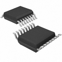
PW PACKAGE
(TOP VIEW)
Qualified for Automotive Applications
Operating Range 2-V to 5.5-V VCC
8-Bit Serial-In, Parallel-Out Shift
Shift Register Has Direct Clear
QB
QC
QD
QE
QF
QG
QH
GND
1
16
2
15
3
14
4
13
5
12
6
11
7
10
8
9
VCC
QA
SER
OE
RCLK
SRCLK
SRCLR
QH′
DESCRIPTION/ORDERING INFORMATION
The SN74AHC595 contains an 8-bit serial-in, parallel-out shift register that feeds an 8-bit D-type storage register.
The storage register has parallel 3-state outputs. Separate clocks are provided for both the shift and storage
registers. The shift register has a direct overriding clear (SRCLR) input, serial (SER) input, and a serial output for
cascading. When the output-enable (OE) input is high, all outputs, except QH', are in the high-impedance state.
Both the shift-register clock (SRCLK) and storage-register clock (RCLK) are positive-edge triggered. If both
clocks are connected together, the shift register always is one clock pulse ahead of the storage register.
ORDERING INFORMATION (1)
PACKAGE (2)
TA
–40°C to 125°C
(1)
(2)
TSSOP – PW
ORDERABLE PART NUMBER
Reel of 2000
SN74AHC595QPWRQ1
TOP-SIDE MARKING
HA595Q
For the most current package and ordering information, see the Package Option Addendum at the end of this document, or see the TI
web site at www.ti.com.
Package drawings, thermal data, and symbolization are available at www.ti.com/packaging.
FUNCTION TABLE
INPUTS
FUNCTION
SER
SRCLK
SRCLR
RCLK
OE
X
X
X
X
H
Outputs QA–QH are disabled.
X
X
X
X
L
Outputs QA–QH are enabled.
X
X
L
X
X
Shift register is cleared.
L
↑
H
X
X
First stage of the shift register goes low.
Other stages store the data of previous stage, respectively.
H
↑
H
X
X
First stage of the shift register goes high.
Other stages store the data of previous stage, respectively.
X
X
X
↑
X
Shift-register data is stored into the storage register.
1
Please be aware that an important notice concerning availability, standard warranty, and use in critical applications of
Texas Instruments semiconductor products and disclaimers thereto appears at the end of this data sheet.
PRODUCTION DATA information is current as of publication date.
Products conform to specifications per the terms of the Texas
Instruments standard warranty. Production processing does not
necessarily include testing of all parameters.
Copyright © 2003–2008, Texas Instruments Incorporated
�SN74AHC595-Q1
8-BIT SHIFT REGISTER
WITH 3-STATE OUTPUT REGISTERS
www.ti.com
SCLS537B – AUGUST 2003 – REVISED JANUARY 2008
LOGIC DIAGRAM (POSITIVE LOGIC)
OE
RCLK
SRCLR
SRCLK
SER
13
12
10
11
14
1D Q
C1
R
3D
C3 Q
15
2D Q
C2
R
3D
C3 Q
1
2D Q
C2
R
3D
C3 Q
2
2D Q
C2
R
3D
C3 Q
3
2D Q
C2
R
3D
C3 Q
4
2D Q
C2
R
3D
C3 Q
5
2D Q
C2
R
3D
C3 Q
6
2D Q
C2
R
3D
C3 Q
7
9
2
Submit Documentation Feedback
QA
QB
QC
QD
QE
QF
QG
QH
QH′
Copyright © 2003–2008, Texas Instruments Incorporated
Product Folder Link(s): SN74AHC595-Q1
�SN74AHC595-Q1
8-BIT SHIFT REGISTER
WITH 3-STATE OUTPUT REGISTERS
www.ti.com
SCLS537B – AUGUST 2003 – REVISED JANUARY 2008
TIMING DIAGRAM
SRCLK
SER
RCLK
SRCLR
ÎÎÎÎ
ÎÎÎÎ
ÎÎÎÎ
ÎÎÎÎ
ÎÎÎÎ
ÎÎÎÎ
ÎÎÎÎ
ÎÎÎÎ
ÎÎÎÎ
ÎÎÎÎ
ÎÎÎÎ
ÎÎÎÎ
ÎÎÎÎ
ÎÎÎÎ
ÎÎÎÎ
ÎÎÎÎ
ÎÎÎÎ
ÎÎÎÎ
OE
QA
QB
QC
QD
QE
QF
QG
QH
QH′
Copyright © 2003–2008, Texas Instruments Incorporated
Product Folder Link(s): SN74AHC595-Q1
Submit Documentation Feedback
3
�SN74AHC595-Q1
8-BIT SHIFT REGISTER
WITH 3-STATE OUTPUT REGISTERS
www.ti.com
SCLS537B – AUGUST 2003 – REVISED JANUARY 2008
ABSOLUTE MAXIMUM RATINGS (1)
over operating free-air temperature range (unless otherwise noted)
VCC
Supply voltage range
VI
Input voltage range (2)
–0.5 V to 7 V
VO
Output voltage range (2)
IIK
Input clamp current
VI < 0
–20 mA
IOK
Output clamp current
VO < 0 or VO > VCC
±20 mA
IO
Continuous output current
VO = 0 to VCC
±25 mA
–0.5 V to 7 V
–0.5 V to VCC + 0.5 V
Continuous current through VCC or GND
±75 mA
θJA
Package thermal impedance, junction to free air (3)
108°C/W
Tstg
Storage temperature range
(1)
(2)
(3)
–65°C to 150°C
Stresses beyond those listed under absolute maximum ratings may cause permanent damage to the device. These are stress ratings
only, and functional operation of the device at these or any other conditions beyond those indicated under recommended operating
conditions is not implied. Exposure to absolute-maximum-rated conditions for extended periods may affect device reliability.
The input and output voltage ratings may be exceeded if the input and output current ratings are observed.
The package thermal impedance is calculated in accordance with JESD 51-7.
RECOMMENDED OPERATING CONDITIONS (1)
VCC
Supply voltage
VIH
High-level input voltage
VCC = 2 V
MIN
MAX
2
5.5
2.1
0.5
VCC = 3 V
0.9
VCC = 5.5 V
VI
Input voltage
VO
Output voltage
High-level output current
IOL
Low-level output current
Δt/Δv
Input transition rise or fall rate
TA
Operating free-air temperature
(1)
4
V
1.65
0
5.5
0
VCC
V
–50
µA
VCC = 2 V
IOH
V
3.85
VCC = 2 V
Low-level input voltage
V
1.5
VCC = 3 V
VCC = 5.5 V
VIL
UNIT
VCC = 3.3 V ± 0.3 V
–4
VCC = 5 V ± 0.5 V
–8
VCC = 2 V
50
VCC = 3.3 V ± 0.3 V
4
VCC = 5 V ± 0.5 V
8
VCC = 3.3 V ± 0.3 V
100
VCC = 5 V ± 0.5 V
20
I-suffix devices
–40
85
Q-suffix devices
–40
125
V
mA
µA
mA
ns/V
°C
All unused inputs of the device must be held at VCC or GND to ensure proper device operation. Refer to the TI application report,
Implications of Slow or Floating CMOS Inputs, literature number SCBA004.
Submit Documentation Feedback
Copyright © 2003–2008, Texas Instruments Incorporated
Product Folder Link(s): SN74AHC595-Q1
�SN74AHC595-Q1
8-BIT SHIFT REGISTER
WITH 3-STATE OUTPUT REGISTERS
www.ti.com
SCLS537B – AUGUST 2003 – REVISED JANUARY 2008
ELECTRICAL CHARACTERISTICS
over recommended operating free-air temperature range (unless otherwise noted)
PARAMETER
TEST CONDITIONS
VCC
IOH = –50 µA
2V
1.9
2
1.9
2.9
3V
2.9
3
4.4
4.5
IOH = –4 mA
3V
2.58
IOH = –8 mA
4.5 V
3.94
IOL = 50 µA
VOL
IOL = 4 mA
IOL = 8 mA
VI = 5.5 V or GND
MAX
MIN
TYP
4.5 V
VOH
II
TA = 25°C
MIN
MAX
4.4
UNIT
V
2.48
3.8
2V
0.1
0.1
3V
0.1
0.1
4.5 V
0.1
0.1
3V
0.36
0.44
V
4.5 V
0.36
0.44
0 V to 5.5 V
±0.1
±1
µA
IOZ
QA–QH, VI = VCC or GND,
VO = VCC or GND, OE = VIH or VIL
5.5 V
±0.25
±10
µA
ICC
VI = VCC or GND, IO = 0
5.5 V
4
40
µA
Ci
VI = VCC or GND
5V
3
10
10
pF
Co
VO = VCC or GND
5V
5.5
pF
TIMING REQUIREMENTS
VCC = 3.3 V ± 0.3 V, over recommended operating free-air temperature range (unless otherwise noted) (see Figure 1)
TA = 25°C
MIN
tw
Pulse duration
5.5
6.5
RCLK high or low
5.5
6.5
5
6
3.5
4.5
8
9.5
8
10
SER before SRCLK↑
Setup time
th
Hold time
SRCLK↑ before RCLK↑
(1)
SRCLR low before RCLK↑
SRCLR high (inactive) before SRCLK↑
(1)
MIN
SRCLK high or low
SRCLR low
tsu
MAX
SER after SRCLK↑
3
4
1.5
2.5
MAX
UNIT
ns
ns
ns
This setup time allows the storage register to receive stable data from the shift register. The clocks can be tied together, in which case
the shift register is one clock pulse ahead of the storage register.
TIMING REQUIREMENTS
VCC = 5 V ± 0.5 V, over recommended operating free-air temperature range (unless otherwise noted) (see Figure 1)
TA = 25°C
MIN
SRCLK high or low
tw
Pulse duration
5
RCLK high or low
SRCLR low
SER before SRCLK↑
tsu
Setup time
SRCLK↑ before RCLK↑
(1)
SRCLR low before RCLK↑
SRCLR high (inactive) before SRCLK↑
th
(1)
Hold time
SER after SRCLK↑
MAX
MIN
MAX
UNIT
6
5
6
5.2
6.2
3
4
5
6
5
6
2.5
3.5
2
3
ns
ns
ns
This setup time allows the storage register to receive stable data from the shift register. The clocks can be tied together, in which case
the shift register is one clock pulse ahead of the storage register.
Copyright © 2003–2008, Texas Instruments Incorporated
Product Folder Link(s): SN74AHC595-Q1
Submit Documentation Feedback
5
�SN74AHC595-Q1
8-BIT SHIFT REGISTER
WITH 3-STATE OUTPUT REGISTERS
www.ti.com
SCLS537B – AUGUST 2003 – REVISED JANUARY 2008
SWITCHING CHARACTERISTICS
VCC = 3.3 V ± 0.3 V, over recommended operating free-air temperature range (unless otherwise noted) (see Figure 1)
PARAMETER
FROM
(INPUT)
TO
(OUTPUT)
fmax
tPLH
tPHL
tPLH
tPHL
tPHL
tPZH
tPZL
tPHZ
tPLZ
TA = 25°C
LOAD
CAPACITANCE
CL = 50 pF
RCLK
QA–QH
CL = 50 pF
SRCLK
QH'
CL = 50 pF
SRCLR
QH'
CL = 50 pF
OE
QA–QH
CL = 50 pF
OE
QA–QH
CL = 50 pF
MIN
TYP
55
105
MAX
MIN
MAX
40
UNIT
MHz
7.9
15.4
1
20
7.9
15.4
1
20
9.2
16.5
1
21.5
9.2
16.5
1
21.5
9
16.3
1
20.2
7.8
15
1
20
9.6
15
1
20
8.1
15.7
1
19.2
9.3
15.7
1
19.2
ns
ns
ns
ns
ns
SWITCHING CHARACTERISTICS
VCC = 5 V ± 0.5 V, over recommended operating free-air temperature range (unless otherwise noted) (see Figure 1)
PARAMETER
FROM
(INPUT)
TO
(OUTPUT)
fmax
tPLH
tPHL
tPLH
tPHL
tPHL
tPZH
tPZL
tPHZ
tPLZ
TA = 25°C
LOAD
CAPACITANCE
CL = 50 pF
RCLK
QA–QH
CL = 50 pF
SRCLK
QH'
CL = 50 pF
SRCLR
QH'
CL = 50 pF
OE
QA–QH
CL = 50 pF
OE
QA–QH
CL = 50 pF
MIN
TYP
95
140
MAX
MIN
MAX
75
UNIT
MHz
5.6
9.4
1
13.5
5.6
9.4
1
13.5
6.4
10.2
1
14.4
6.4
10.2
1
14.4
6.4
10
1
14.1
5.7
10.6
1
15
6.8
10.6
1
15
3.5
10.3
1
14
3.4
10.3
1
14
ns
ns
ns
ns
ns
OPERATING CHARACTERISTICS
VCC = 5 V, TA = 25°C (unless otherwise noted)
PARAMETER
Cpd
6
Power dissipation capacitance
TEST CONDITIONS
No load, f = 10 MHz
Submit Documentation Feedback
TYP
UNIT
114
pF
Copyright © 2003–2008, Texas Instruments Incorporated
Product Folder Link(s): SN74AHC595-Q1
�SN74AHC595-Q1
8-BIT SHIFT REGISTER
WITH 3-STATE OUTPUT REGISTERS
www.ti.com
SCLS537B – AUGUST 2003 – REVISED JANUARY 2008
PARAMETER MEASUREMENT INFORMATION
VCC
From Output
Under Test
Test
Point
RL = 1 kΩ
From Output
Under Test
CL
(see Note A)
S1
Open
TEST
GND
CL
(see Note A)
LOAD CIRCUIT FOR
TOTEM-POLE OUTPUTS
S1
tPLH/tPHL
tPLZ/tPZL
tPHZ/tPZH
Open Drain
Open
VCC
GND
VCC
LOAD CIRCUIT FOR
3-STATE AND OPEN-DRAIN OUTPUTS
VCC
50% VCC
Timing Input
tw
tsu
VCC
50% VCC
Input
50% VCC
0V
th
VCC
50% VCC
Data Input
50% VCC
0V
0V
VOLTAGE WAVEFORMS
PULSE DURATION
VOLTAGE WAVEFORMS
SETUP AND HOLD TIMES
VCC
50% VCC
Input
50% VCC
0V
tPLH
In-Phase
Output
tPHL
VOH
50% VCC
VOL
50% VCC
tPHL
Out-of-Phase
Output
Output
Waveform 1
S1 at VCC
(see Note B)
VOH
50% VCC
VOL
50% VCC
tPZL
tPLZ
≈VCC
50% VCC
VOL + 0.3 V
VOL
tPHZ
Output
Waveform 2
S1 at GND
(see Note B)
VOLTAGE WAVEFORMS
PROPAGATION DELAY TIMES
INVERTING AND NONINVERTING OUTPUTS
50% VCC
0V
tPZH
tPLH
50% VCC
VCC
Output
Control
50% VCC
VOH − 0.3 V
VOH
≈0 V
VOLTAGE WAVEFORMS
ENABLE AND DISABLE TIMES
LOW- AND HIGH-LEVEL ENABLING
NOTES: A. CL includes probe and jig capacitance.
B. Waveform 1 is for an output with internal conditions such that the output is low, except when disabled by the output control.
Waveform 2 is for an output with internal conditions such that the output is high, except when disabled by the output control.
C. All input pulses are supplied by generators having the following characteristics: PRR ≤ 1 MHz, ZO = 50 Ω, tr ≤ 3 ns, tf ≤ 3 ns.
D. The outputs are measured one at a time, with one input transition per measurement.
Figure 1. Load Circuit and Voltage Waveforms
Copyright © 2003–2008, Texas Instruments Incorporated
Product Folder Link(s): SN74AHC595-Q1
Submit Documentation Feedback
7
�PACKAGE OPTION ADDENDUM
www.ti.com
10-Dec-2020
PACKAGING INFORMATION
Orderable Device
Status
(1)
Package Type Package Pins Package
Drawing
Qty
Eco Plan
(2)
Lead finish/
Ball material
MSL Peak Temp
Op Temp (°C)
Device Marking
(3)
(4/5)
(6)
SN74AHC595QPWRQ1
ACTIVE
TSSOP
PW
16
2000
RoHS & Green
NIPDAU
Level-1-260C-UNLIM
-40 to 125
HA595Q
(1)
The marketing status values are defined as follows:
ACTIVE: Product device recommended for new designs.
LIFEBUY: TI has announced that the device will be discontinued, and a lifetime-buy period is in effect.
NRND: Not recommended for new designs. Device is in production to support existing customers, but TI does not recommend using this part in a new design.
PREVIEW: Device has been announced but is not in production. Samples may or may not be available.
OBSOLETE: TI has discontinued the production of the device.
(2)
RoHS: TI defines "RoHS" to mean semiconductor products that are compliant with the current EU RoHS requirements for all 10 RoHS substances, including the requirement that RoHS substance
do not exceed 0.1% by weight in homogeneous materials. Where designed to be soldered at high temperatures, "RoHS" products are suitable for use in specified lead-free processes. TI may
reference these types of products as "Pb-Free".
RoHS Exempt: TI defines "RoHS Exempt" to mean products that contain lead but are compliant with EU RoHS pursuant to a specific EU RoHS exemption.
Green: TI defines "Green" to mean the content of Chlorine (Cl) and Bromine (Br) based flame retardants meet JS709B low halogen requirements of


 工商网监
湘ICP备2023018690号
工商网监
湘ICP备2023018690号
