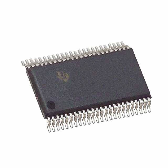
SN54AHCT16240, SN74AHCT16240
16-BIT BUFFERS/DRIVERS
WITH 3-STATE OUTPUTS
SCLS333I – MARCH 1996 – REVISED JANUARY 2000
D
D
D
D
D
D
D
D
SN54AHCT16240 . . . WD PACKAGE
SN74AHCT16240 . . . DGG, DGV, OR DL PACKAGE
(TOP VIEW)
Members of the Texas Instruments
Widebus Family
EPIC (Enhanced-Performance Implanted
CMOS) Process
Inputs Are TTL-Voltage Compatible
Distributed VCC and GND Pins Minimize
High-Speed Switching Noise
Flow-Through Architecture Optimizes PCB
Layout
Latch-Up Performance Exceeds 250 mA Per
JESD 17
ESD Protection Exceeds 2000 V Per
MIL-STD-883, Method 3015
Package Options Include Plastic Shrink
Small-Outline (DL), Thin Shrink
Small-Outline (DGG), and Thin Very
Small-Outline (DGV) Packages and 380-mil
Fine-Pitch Ceramic Flat (WD) Package
Using 25-mil Center-to-Center Spacings
1OE
1Y1
1Y2
GND
1Y3
1Y4
VCC
2Y1
2Y2
GND
2Y3
2Y4
3Y1
3Y2
GND
3Y3
3Y4
VCC
4Y1
4Y2
GND
4Y3
4Y4
4OE
description
The ’AHCT16240 devices are 16-bit buffers and
line drivers designed specifically to improve the
performance and density of 3-state memory
address drivers, clock drivers, and bus-oriented
receivers and transmitters.
1
48
2
47
3
46
4
45
5
44
6
43
7
42
8
41
9
40
10
39
11
38
12
37
13
36
14
35
15
34
16
33
17
32
18
31
19
30
20
29
21
28
22
27
23
26
24
25
2OE
1A1
1A2
GND
1A3
1A4
VCC
2A1
2A2
GND
2A3
2A4
3A1
3A2
GND
3A3
3A4
VCC
4A1
4A2
GND
4A3
4A4
3OE
These devices can be used as four 4-bit buffers,
two 8-bit buffers, or one 16-bit buffer. They provide
inverting outputs and symmetrical active-low
output-enable (OE) inputs.
To ensure the high-impedance state during power up or power down, OE should be tied to VCC through a pullup
resistor; the minimum value of the resistor is determined by the current-sinking capability of the driver.
The SN54AHCT16240 is characterized for operation over the full military temperature range of –55°C to 125°C.
The SN74AHCT16240 is characterized for operation from –40°C to 85°C.
FUNCTION TABLE
(each 4-bit buffer/driver)
INPUTS
OE
A
OUTPUT
Y
L
H
L
L
L
H
H
X
Z
Please be aware that an important notice concerning availability, standard warranty, and use in critical applications of
Texas Instruments semiconductor products and disclaimers thereto appears at the end of this data sheet.
EPIC and Widebus are trademarks of Texas Instruments Incorporated.
Copyright 2000, Texas Instruments Incorporated
UNLESS OTHERWISE NOTED this document contains PRODUCTION
DATA information current as of publication date. Products conform to
specifications per the terms of Texas Instruments standard warranty.
Production processing does not necessarily include testing of all
parameters.
POST OFFICE BOX 655303
• DALLAS, TEXAS 75265
1
�SN54AHCT16240, SN74AHCT16240
16-BIT BUFFERS/DRIVERS
WITH 3-STATE OUTPUTS
SCLS333I – MARCH 1996 – REVISED JANUARY 2000
logic symbol†
1OE
2OE
3OE
4OE
1A1
1A2
1A3
1A4
2A1
2A2
2A3
2A4
3A1
3A2
3A3
3A4
4A1
4A2
4A3
4A4
1
EN1
48
25
24
EN2
EN3
EN4
47
1
1
46
3
44
5
43
6
41
8
1
2
40
9
38
11
37
12
36
1
3
13
35
14
33
16
32
17
30
19
1
4
29
20
27
22
26
23
† This symbol is in accordance with ANSI/IEEE Std 91-1984 and IEC Publication 617-12.
2
2
POST OFFICE BOX 655303
• DALLAS, TEXAS 75265
1Y1
1Y2
1Y3
1Y4
2Y1
2Y2
2Y3
2Y4
3Y1
3Y2
3Y3
3Y4
4Y1
4Y2
4Y3
4Y4
�SN54AHCT16240, SN74AHCT16240
16-BIT BUFFERS/DRIVERS
WITH 3-STATE OUTPUTS
SCLS333I – MARCH 1996 – REVISED JANUARY 2000
logic diagram (positive logic)
1OE
1A1
1A2
1A3
1A4
2OE
2A1
2A2
2A3
2A4
1
3OE
47
2
46
3
44
5
43
6
1Y1
3A1
1Y2
3A2
1Y3
3A3
1Y4
3A4
48
4OE
41
8
40
9
38
11
37
12
2Y1
4A1
2Y2
4A2
2Y3
4A3
2Y4
4A4
25
36
13
35
14
33
16
32
17
3Y1
3Y2
3Y3
3Y4
24
30
19
29
20
27
22
26
23
4Y1
4Y2
4Y3
4Y4
absolute maximum ratings over operating free-air temperature range (unless otherwise noted)†
Supply voltage range, VCC . . . . . . . . . . . . . . . . . . . . . . . . . . . . . . . . . . . . . . . . . . . . . . . . . . . . . . . . . . –0.5 V to 7 V
Input voltage range, VI (see Note 1) . . . . . . . . . . . . . . . . . . . . . . . . . . . . . . . . . . . . . . . . . . . . . . . . . . –0.5 V to 7 V
Output voltage range, VO (see Note 1) . . . . . . . . . . . . . . . . . . . . . . . . . . . . . . . . . . . . . . . . –0.5 V to VCC + 0.5 V
Input clamp current, IIK (VI < 0) . . . . . . . . . . . . . . . . . . . . . . . . . . . . . . . . . . . . . . . . . . . . . . . . . . . . . . . . . . . –20 mA
Output clamp current, IOK (VO < 0 or VO > VCC) . . . . . . . . . . . . . . . . . . . . . . . . . . . . . . . . . . . . . . . . . . . . ±20 mA
Continuous output current, IO (VO = 0 to VCC) . . . . . . . . . . . . . . . . . . . . . . . . . . . . . . . . . . . . . . . . . . . . . . ±25 mA
Continuous current through each VCC or GND . . . . . . . . . . . . . . . . . . . . . . . . . . . . . . . . . . . . . . . . . . . . . . ±75 mA
Package thermal impedance, θJA (see Note 2): DGG package . . . . . . . . . . . . . . . . . . . . . . . . . . . . . . . 70°C/W
DGV package . . . . . . . . . . . . . . . . . . . . . . . . . . . . . . . . 58°C/W
DL package . . . . . . . . . . . . . . . . . . . . . . . . . . . . . . . . . 63°C/W
Storage temperature range, Tstg . . . . . . . . . . . . . . . . . . . . . . . . . . . . . . . . . . . . . . . . . . . . . . . . . . . –65°C to 150°C
† Stresses beyond those listed under “absolute maximum ratings” may cause permanent damage to the device. These are stress ratings only, and
functional operation of the device at these or any other conditions beyond those indicated under “recommended operating conditions” is not
implied. Exposure to absolute-maximum-rated conditions for extended periods may affect device reliability.
NOTES: 1. The input and output voltage ratings may be exceeded if the input and output current ratings are observed.
2. The package thermal impedance is calculated in accordance with JESD 51.
POST OFFICE BOX 655303
• DALLAS, TEXAS 75265
3
�SN54AHCT16240, SN74AHCT16240
16-BIT BUFFERS/DRIVERS
WITH 3-STATE OUTPUTS
SCLS333I – MARCH 1996 – REVISED JANUARY 2000
recommended operating conditions (see Note 3)
SN54AHCT16240
SN74AHCT16240
MIN
MAX
MIN
MAX
4.5
5.5
4.5
5.5
UNIT
VCC
VIH
Supply voltage
VIL
VI
Low-level input voltage
0.8
V
Input voltage
0
5.5
0
5.5
V
VO
IOH
Output voltage
0
0
VCC
–8
V
High-level output current
VCC
–8
mA
IOL
∆t/∆v
Low-level output current
8
8
mA
20
20
ns/V
High-level input voltage
2
2
0.8
Input transition rise or fall rate
V
V
TA
Operating free-air temperature
–55
125
–40
85
°C
NOTE 3: All unused inputs of the device must be held at VCC or GND to ensure proper device operation. Refer to the TI application report,
Implications of Slow or Floating CMOS Inputs, literature number SCBA004.
electrical characteristics over recommended operating free-air temperature range (unless
otherwise noted)
PARAMETER
TEST CONDITIONS
VCC
VOH
IOH = –50 mA
IOH = –8 mA
45V
4.5
VOL
IOL = 50 mA
IOL = 8 mA
45V
4.5
II
IOZ
VI = VCC or GND
VO = VCC or GND
ICC
VI = VCC or GND,
IO = 0
One input at 3.4 V,
Other inputs at VCC or GND
∆ICC†
Ci
VI = VCC or GND
VO = VCC or GND
MIN
4.4
TA = 25°C
TYP
MAX
4.5
3.94
SN54AHCT16240
MIN
MAX
SN74AHCT16240
MIN
4.4
4.4
3.8
3.8
UNIT
V
0.1
0.1
0.1
0.36
0.44
0.44
V
0 V to 5.5 V
±0.1
±1*
±1
mA
5.5 V
±0.25
±2.5
±2.5
mA
5.5 V
4
40
40
mA
5.5 V
1.35
1.5
1.5
mA
10
pF
5V
2.5
10
Co
5V
3
* On products compliant to MIL-PRF-38535, this parameter is not production tested at VCC = 0 V.
† This is the increase in supply current for each input at one of the specified TTL voltage levels rather than 0 V or VCC.
PRODUCT PREVIEW information concerns products in the formative or
design phase of development. Characteristic data and other
specifications are design goals. Texas Instruments reserves the right to
change or discontinue these products without notice.
4
MAX
POST OFFICE BOX 655303
• DALLAS, TEXAS 75265
pF
�SN54AHCT16240, SN74AHCT16240
16-BIT BUFFERS/DRIVERS
WITH 3-STATE OUTPUTS
SCLS333I – MARCH 1996 – REVISED JANUARY 2000
switching characteristics over recommended operating free-air temperature range,
VCC = 5 V ± 0.5 V (unless otherwise noted) (see Figure 1)
PARAMETER
FROM
(INPUT)
TO
(OUTPUT)
LOAD
CAPACITANCE
tPLH
tPHL
A
Y
CL = 15 pF
tPZH
tPZL
OE
Y
CL = 15 pF
tPHZ
tPLZ
OE
Y
CL = 15 pF
tPLH
tPHL
A
Y
CL = 50 pF
tPZH
tPZL
OE
Y
CL = 50 pF
tPHZ
tPLZ
OE
Y
CL = 50 pF
tsk(o)
MIN
TA = 25°C
TYP
MAX
SN54AHCT16240
SN74AHCT16240
MIN
MAX
MIN
MAX
5.4*
8.5*
1*
10*
1
9.5
5.4*
8.5*
1*
10*
1
9.5
7.7*
10.4*
1*
12*
1
12
7.7*
10.4*
1*
12*
1
12
8.3*
10.4*
1*
12*
1
12
8.3*
10.4*
1*
12*
1
12
7
9.5
1
11
1
10.5
5.9
9.5
1
11
1
10.5
8.2
11.4
1
13
1
13
8.2
11.4
1
13
1
13
8.8
11.4
1
13
1
13
8.8
11.4
1
13
1
13
1**
CL = 50 pF
1
UNIT
ns
ns
ns
ns
ns
ns
ns
* On products compliant to MIL-PRF-38535, this parameter is not production tested.
** On products compliant to MIL-PRF-38535, this parameter does not apply.
noise characteristics, VCC = 5 V, CL = 50 pF, TA = 25°C (see Note 4)
SN74AHCT16240
PARAMETER
MIN
TYP
MAX
UNIT
VOL(P)
VOL(V)
Quiet output, maximum dynamic VOL
0.6
V
Quiet output, minimum dynamic VOL
–0.6
V
VOH(V)
VIH(D)
Quiet output, minimum dynamic VOH
4.6
V
High-level dynamic input voltage
2
VIL(D)
Low-level dynamic input voltage
NOTE 4: Characteristics are for surface-mount packages only.
V
0.8
V
TYP
UNIT
operating characteristics, VCC = 5 V, TA = 25°C
PARAMETER
Cpd
TEST CONDITIONS
Power dissipation capacitance
No load,
f = 1 MHz
10
pF
PRODUCT PREVIEW information concerns products in the formative or
design phase of development. Characteristic data and other
specifications are design goals. Texas Instruments reserves the right to
change or discontinue these products without notice.
POST OFFICE BOX 655303
• DALLAS, TEXAS 75265
5
�SN54AHCT16240, SN74AHCT16240
16-BIT BUFFERS/DRIVERS
WITH 3-STATE OUTPUTS
SCLS333I – MARCH 1996 – REVISED JANUARY 2000
PARAMETER MEASUREMENT INFORMATION
RL = 1 kΩ
From Output
Under Test
Test
Point
From Output
Under Test
S1
VCC
Open
TEST
GND
CL
(see Note A)
CL
(see Note A)
S1
tPLH/tPHL
tPLZ/tPZL
tPHZ/tPZH
Open Drain
Open
VCC
GND
VCC
LOAD CIRCUIT FOR
3-STATE AND OPEN-DRAIN OUTPUTS
LOAD CIRCUIT FOR
TOTEM-POLE OUTPUTS
3V
1.5 V
Timing Input
0V
tw
3V
1.5 V
Input
1.5 V
th
tsu
3V
1.5 V
Data Input
1.5 V
0V
0V
VOLTAGE WAVEFORMS
PULSE DURATION
VOLTAGE WAVEFORMS
SETUP AND HOLD TIMES
3V
1.5 V
Input
1.5 V
0V
tPLH
In-Phase
Output
tPHL
50% VCC
tPHL
Out-of-Phase
Output
VOH
50% VCC
VOL
Output
Waveform 1
S1 at VCC
(see Note B)
VOH
50% VCC
VOL
1.5 V
tPLZ
≈VCC
50% VCC
Output
Waveform 2
S1 at GND
(see Note B)
VOLTAGE WAVEFORMS
PROPAGATION DELAY TIMES
INVERTING AND NONINVERTING OUTPUTS
1.5 V
0V
tPZL
tPZH
tPLH
50% VCC
3V
Output
Control
VOL + 0.3 V
VOL
tPHZ
50% VCC
VOH – 0.3 V
VOH
≈0 V
VOLTAGE WAVEFORMS
ENABLE AND DISABLE TIMES
LOW- AND HIGH-LEVEL ENABLING
NOTES: A. CL includes probe and jig capacitance.
B. Waveform 1 is for an output with internal conditions such that the output is low except when disabled by the output control.
Waveform 2 is for an output with internal conditions such that the output is high except when disabled by the output control.
C. All input pulses are supplied by generators having the following characteristics: PRR ≤ 1 MHz, ZO = 50 Ω, tr ≤ 3 ns, tf ≤ 3 ns.
D. The outputs are measured one at a time with one input transition per measurement.
Figure 1. Load Circuit and Voltage Waveforms
6
POST OFFICE BOX 655303
• DALLAS, TEXAS 75265
�PACKAGE OPTION ADDENDUM
www.ti.com
10-Dec-2020
PACKAGING INFORMATION
Orderable Device
Status
(1)
Package Type Package Pins Package
Drawing
Qty
Eco Plan
(2)
Lead finish/
Ball material
MSL Peak Temp
Op Temp (°C)
Device Marking
(3)
(4/5)
(6)
SN74AHCT16240DGGR
ACTIVE
TSSOP
DGG
48
2000
RoHS & Green
NIPDAU
Level-1-260C-UNLIM
-40 to 85
AHCT16240
SN74AHCT16240DGVR
ACTIVE
TVSOP
DGV
48
2000
RoHS & Green
NIPDAU
Level-1-260C-UNLIM
-40 to 85
HF240
SN74AHCT16240DL
ACTIVE
SSOP
DL
48
25
RoHS & Green
NIPDAU
Level-1-260C-UNLIM
-40 to 85
AHCT16240
SN74AHCT16240DLR
ACTIVE
SSOP
DL
48
1000
RoHS & Green
NIPDAU
Level-1-260C-UNLIM
-40 to 85
AHCT16240
(1)
The marketing status values are defined as follows:
ACTIVE: Product device recommended for new designs.
LIFEBUY: TI has announced that the device will be discontinued, and a lifetime-buy period is in effect.
NRND: Not recommended for new designs. Device is in production to support existing customers, but TI does not recommend using this part in a new design.
PREVIEW: Device has been announced but is not in production. Samples may or may not be available.
OBSOLETE: TI has discontinued the production of the device.
(2)
RoHS: TI defines "RoHS" to mean semiconductor products that are compliant with the current EU RoHS requirements for all 10 RoHS substances, including the requirement that RoHS substance
do not exceed 0.1% by weight in homogeneous materials. Where designed to be soldered at high temperatures, "RoHS" products are suitable for use in specified lead-free processes. TI may
reference these types of products as "Pb-Free".
RoHS Exempt: TI defines "RoHS Exempt" to mean products that contain lead but are compliant with EU RoHS pursuant to a specific EU RoHS exemption.
Green: TI defines "Green" to mean the content of Chlorine (Cl) and Bromine (Br) based flame retardants meet JS709B low halogen requirements of


 工商网监
湘ICP备2023018690号
工商网监
湘ICP备2023018690号
