SN54AHCT374, SN74AHCT374
OCTAL EDGE-TRIGGERED D-TYPE FLIP-FLOPS
WITH 3-STATE OUTPUTS
SCLS241L – OCTOBER 1995 – REVISED JULY 2003
D
D
D
Inputs Are TTL-Voltage Compatible
Latch-Up Performance Exceeds 250 mA Per
JESD 17
ESD Protection Exceeds JESD 22
– 2000-V Human-Body Model (A114-A)
– 200-V Machine Model (A115-A)
– 1000-V Charged-Device Model (C101)
SN54AHCT374 . . . J OR W PACKAGE
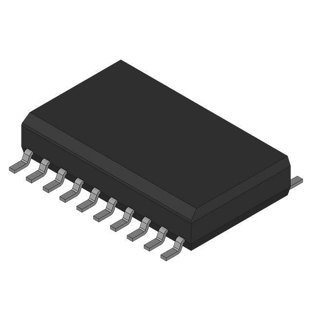
SN74AHCT374 . . . DB, DGV, DW, N, NS, OR PW PACKAGE
(TOP VIEW)
1
20
2
19
3
18
4
17
5
16
6
15
7
14
8
13
9
12
10
11
1D
1Q
OE
VCC
8Q
VCC
8Q
8D
7D
7Q
6Q
6D
5D
5Q
CLK
2D
2Q
3Q
3D
4D
4
3 2
1 20 19
18
5
17
6
16
7
15
8
14
9 10 11 12 13
8D
7D
7Q
6Q
6D
4Q
GND
CLK
5Q
5D
OE
1Q
1D
2D
2Q
3Q
3D
4D
4Q
GND
SN54AHCT374 . . . FK PACKAGE
(TOP VIEW)
description/ordering information
The ’AHCT374 devices are octal edge-triggered D-type flip-flops that feature 3-state outputs designed
specifically for driving highly capacitive or relatively low-impedance loads. This device is particularly suitable
for implementing buffer registers, I/O ports, bidirectional bus drivers, and working registers.
On the positive transition of the clock (CLK) input, the Q outputs are set to the logic levels of the data (D) inputs.
A buffered output-enable (OE) input can be used to place the eight outputs in either a normal logic state (high
or low logic levels) or the high-impedance state. In the high-impedance state, the outputs neither load nor drive
the bus lines significantly. The high-impedance state and the increased drive provide the capability to drive bus
lines without interface or pullup components.
ORDERING INFORMATION
PDIP – N
SN74AHCT374N
Tube
SN74AHCT374DW
Tape and reel
SN74AHCT374DWR
SOP – NS
Tape and reel
SN74AHCT374NSR
AHCT374
SSOP – DB
Tape and reel
SN74AHCT374DBR
HB374
Tube
SN74AHCT374PW
Tape and reel
SN74AHCT374PWR
TVSOP – DGV
Tape and reel
SN74AHCT374DGVR
HB374
CDIP – J
Tube
SNJ54AHCT374J
SNJ54AHCT374J
CFP – W
Tube
SNJ54AHCT374W
SNJ54AHCT374W
LCCC – FK
Tube
SNJ54AHCT374FK
SNJ54AHCT374FK
TSSOP – PW
–55°C to 125°C
TOP-SIDE
MARKING
Tube
SOIC – DW
–40°C
40°C to 85°C
ORDERABLE
PART NUMBER
PACKAGE†
TA
SN74AHCT374N
AHCT374
HB374
† Package drawings, standard packing quantities, thermal data, symbolization, and PCB design guidelines
are available at www.ti.com/sc/package.
Please be aware that an important notice concerning availability, standard warranty, and use in critical applications of
Texas Instruments semiconductor products and disclaimers thereto appears at the end of this data sheet.
Copyright 2003, Texas Instruments Incorporated
PRODUCTION DATA information is current as of publication date.
Products conform to specifications per the terms of Texas Instruments
standard warranty. Production processing does not necessarily include
testing of all parameters.
On products compliant to MIL-PRF-38535, all parameters are tested
unless otherwise noted. On all other products, production
processing does not necessarily include testing of all parameters.
POST OFFICE BOX 655303
• DALLAS, TEXAS 75265
1
�SN54AHCT374, SN74AHCT374
OCTAL EDGE-TRIGGERED D-TYPE FLIP-FLOPS
WITH 3-STATE OUTPUTS
SCLS241L – OCTOBER 1995 – REVISED JULY 2003
description/ordering information (continued)
OE does not affect internal operations of the flip-flop. Old data can be retained or new data can be entered while
the outputs are in the high-impedance state.
To ensure the high-impedance state during power up or power down, OE should be tied to VCC through a pullup
resistor; the minimum value of the resistor is determined by the current-sinking capability of the driver.
FUNCTION TABLE
(each flip-flop)
INPUTS
OE
CLK
D
OUTPUT
Q
L
↑
H
H
L
↑
L
L
L
H or L
X
Q0
H
X
X
Z
logic diagram (positive logic)
OE
CLK
1
11
C1
1D
3
1D
2
1Q
To Seven Other Channels
absolute maximum ratings over operating free-air temperature range (unless otherwise noted)†
Supply voltage range, VCC . . . . . . . . . . . . . . . . . . . . . . . . . . . . . . . . . . . . . . . . . . . . . . . . . . . . . . . . . –0.5 V to 7 V
Input voltage range, VI (see Note 1) . . . . . . . . . . . . . . . . . . . . . . . . . . . . . . . . . . . . . . . . . . . . . . . . . . –0.5 V to 7 V
Output voltage range, VO (see Note 1) . . . . . . . . . . . . . . . . . . . . . . . . . . . . . . . . . . . . . . . . –0.5 V to VCC + 0.5 V
Input clamp current, IIK (VI < 0) . . . . . . . . . . . . . . . . . . . . . . . . . . . . . . . . . . . . . . . . . . . . . . . . . . . . . . . . . . . –20 mA
Output clamp current, IOK (VO < 0 or VO > VCC) . . . . . . . . . . . . . . . . . . . . . . . . . . . . . . . . . . . . . . . . . . . . ±20 mA
Continuous output current, IO (VO = 0 to VCC) . . . . . . . . . . . . . . . . . . . . . . . . . . . . . . . . . . . . . . . . . . . . . . ±25 mA
Continuous current through VCC or GND . . . . . . . . . . . . . . . . . . . . . . . . . . . . . . . . . . . . . . . . . . . . . . . . . . . ±75 mA
Package thermal impedance, θJA (see Note 2): DB package . . . . . . . . . . . . . . . . . . . . . . . . . . . . . . . . . 70°C/W
DGV package . . . . . . . . . . . . . . . . . . . . . . . . . . . . . . . . 92°C/W
DW package . . . . . . . . . . . . . . . . . . . . . . . . . . . . . . . . . 58°C/W
N package . . . . . . . . . . . . . . . . . . . . . . . . . . . . . . . . . . . 69°C/W
NS package . . . . . . . . . . . . . . . . . . . . . . . . . . . . . . . . . 60°C/W
PW package . . . . . . . . . . . . . . . . . . . . . . . . . . . . . . . . . 83°C/W
Storage temperature range, Tstg . . . . . . . . . . . . . . . . . . . . . . . . . . . . . . . . . . . . . . . . . . . . . . . . . . . –65°C to 150°C
† Stresses beyond those listed under “absolute maximum ratings” may cause permanent damage to the device. These are stress ratings only, and
functional operation of the device at these or any other conditions beyond those indicated under “recommended operating conditions” is not
implied. Exposure to absolute-maximum-rated conditions for extended periods may affect device reliability.
NOTES: 1. The input and output voltage ratings may be exceeded if the input and output current ratings are observed.
2. The package thermal impedance is calculated in accordance with JESD 51-7.
2
POST OFFICE BOX 655303
• DALLAS, TEXAS 75265
�SN54AHCT374, SN74AHCT374
OCTAL EDGE-TRIGGERED D-TYPE FLIP-FLOPS
WITH 3-STATE OUTPUTS
SCLS241L – OCTOBER 1995 – REVISED JULY 2003
recommended operating conditions (see Note 3)
SN54AHCT374
SN74AHCT374
MIN
MAX
MIN
MAX
4.5
5.5
4.5
5.5
UNIT
VCC
VIH
Supply voltage
VIL
VI
Low-level input voltage
0.8
V
Input voltage
0
5.5
0
5.5
V
VO
IOH
Output voltage
0
0
VCC
–8
V
High-level output current
VCC
–8
mA
IOL
∆t/∆v
Low-level output current
8
8
mA
20
20
ns/V
High-level input voltage
2
2
0.8
Input transition rise or fall rate
V
V
TA
Operating free-air temperature
–55
125
–40
85
°C
NOTE 3: All unused inputs of the device must be held at VCC or GND to ensure proper device operation. Refer to the TI application report,
Implications of Slow or Floating CMOS Inputs, literature number SCBA004.
electrical characteristics over recommended operating free-air temperature range (unless
otherwise noted)
PARAMETER
TEST CONDITIONS
VCC
VOH
IOH = –50 mA
IOH = –8 mA
45V
4.5
VOL
IOL = 50 mA
IOL = 8 mA
45V
4.5
II
IOZ
VI = 5.5 V or GND
VO = VCC or GND,
ICC
VI = VCC or GND,
One input at 3.4 V,
Other inputs at VCC or GND
∆ICC†
Ci
Co
VI = VIH or VIL
IO = 0
VI = VCC or GND
VO = VCC or GND
TA = 25°C
TYP MAX
MIN
4.4
4.5
3.94
SN54AHCT374
MIN
MAX
SN74AHCT374
MIN
4.4
4.4
3.8
3.8
MAX
UNIT
V
0.1
0.1
0.1
0.36
0.44
0.44
V
0 V to 5.5 V
±0.1
±1*
±1
mA
5.5 V
±0.25
±2.5
±2.5
mA
5.5 V
4
40
40
mA
5.5 V
1.35
1.5
1.5
mA
10
pF
5V
4
5V
9
10
pF
* On products compliant to MIL-PRF-38535, this parameter is not production tested at VCC = 0 V.
† This is the increase in supply current for each input at one of the specified TTL voltage levels, rather than 0 V or VCC.
timing requirements over recommended operating free-air temperature range, VCC = 5 V ± 0.5 V
(unless otherwise noted) (see Figure 1)
TA = 25°C
MIN
MAX
SN54AHCT374
MIN
MAX
SN74AHCT374
MIN
MAX
UNIT
tw
Pulse duration, CLK high or low
6.5
6.5
6.5
ns
tsu
Setup time, data before CLK↑
2.5
2.5
2.5
ns
th
Hold time, data after CLK↑
2.5
2.5
2.5
ns
POST OFFICE BOX 655303
• DALLAS, TEXAS 75265
3
�SN54AHCT374, SN74AHCT374
OCTAL EDGE-TRIGGERED D-TYPE FLIP-FLOPS
WITH 3-STATE OUTPUTS
SCLS241L – OCTOBER 1995 – REVISED JULY 2003
switching characteristics over recommended free-air temperature operating range,
VCC = 5 V ± 0.5 V (unless otherwise noted) (see Figure 1)
PARAMETER
FROM
(INPUT)
TO
(OUTPUT)
fmax
TA = 25°C
TYP
MAX
SN54AHCT374
SN74AHCT374
LOAD
CAPACITANCE
MIN
CL = 15 pF
90**
140**
80**
80
CL = 50 pF
85
130
75
75
tPLH
tPHL
CLK
Q
CL = 15 pF
tPZH
tPZL
OE
Q
CL = 15 pF
tPHZ
tPLZ
OE
Q
CL = 15 pF
tPLH
tPHL
CLK
Q
CL = 50 pF
tPZH
tPZL
OE
Q
CL = 50 pF
tPHZ
tPLZ
OE
Q
CL = 50 pF
MIN
MAX
MIN
MAX
MHz
5.6**
9.4**
1**
10.5**
1
10.5
5.6**
9.4**
1**
10.5**
1
10.5
6.5**
10.2**
1**
11.5**
1
11.5
6.5**
10.2**
1**
11.5**
1
11.5
6.2**
10.2**
1**
11**
1
11
6.2**
10.2**
1**
11**
1
11
6.4
10.4
1
11.5
1
11.5
6.4
10.4
1
11.5
1
11.5
7.3
11.2
1
12.5
1
12.5
7.3
11.2
1
12.5
1
12.5
7
11.2
1
12
1
12
7
11.2
1
12
1
12
tsk(o)
CL = 50 pF
** On products compliant to MIL-PRF-38535, this parameter is not production tested.
*** On products compliant to MIL-PRF-38535, this parameter does not apply.
UNIT
1***
1
ns
ns
ns
ns
ns
ns
ns
noise characteristics, VCC = 5 V, CL = 50 pF, TA = 25°C (see Note 4)
SN74AHCT374
PARAMETER
MIN
TYP
MAX
UNIT
VOL(P)
VOL(V)
Quiet output, maximum dynamic VOL
0.8
1.2
V
Quiet output, minimum dynamic VOL
–0.8
–1.2
V
VOH(V)
VIH(D)
Quiet output, minimum dynamic VOH
VIL(D)
Low-level dynamic input voltage
3.8
High-level dynamic input voltage
V
2
V
0.8
V
TYP
UNIT
NOTE 4: Characteristics are for surface-mount packages only.
operating characteristics, VCC = 5 V, TA = 25°C
PARAMETER
Cpd
4
TEST CONDITIONS
Power dissipation capacitance
No load,
POST OFFICE BOX 655303
• DALLAS, TEXAS 75265
f = 1 MHz
27
pF
�SN54AHCT374, SN74AHCT374
OCTAL EDGE-TRIGGERED D-TYPE FLIP-FLOPS
WITH 3-STATE OUTPUTS
SCLS241L – OCTOBER 1995 – REVISED JULY 2003
PARAMETER MEASUREMENT INFORMATION
From Output
Under Test
Test
Point
RL = 1 kΩ
From Output
Under Test
VCC
Open
S1
TEST
GND
CL
(see Note A)
CL
(see Note A)
S1
tPLH/tPHL
tPLZ/tPZL
tPHZ/tPZH
Open Drain
Open
VCC
GND
VCC
LOAD CIRCUIT FOR
3-STATE AND OPEN-DRAIN OUTPUTS
LOAD CIRCUIT FOR
TOTEM-POLE OUTPUTS
3V
1.5 V
Timing Input
0V
tw
3V
1.5 V
Input
1.5 V
th
tsu
3V
1.5 V
Data Input
1.5 V
0V
0V
VOLTAGE WAVEFORMS
PULSE DURATION
VOLTAGE WAVEFORMS
SETUP AND HOLD TIMES
3V
1.5 V
Input
1.5 V
0V
tPLH
In-Phase
Output
tPHL
50% VCC
tPHL
Out-of-Phase
Output
VOH
50% VCC
VOL
Output
Waveform 1
S1 at VCC
(see Note B)
VOH
50% VCC
VOL
VOLTAGE WAVEFORMS
PROPAGATION DELAY TIMES
INVERTING AND NONINVERTING OUTPUTS
1.5 V
1.5 V
0V
tPZL
tPLZ
≈VCC
50% VCC
tPZH
tPLH
50% VCC
3V
Output
Control
Output
Waveform 2
S1 at GND
(see Note B)
VOL + 0.3 V
VOL
tPHZ
50% VCC
VOH – 0.3 V
VOH
≈0 V
VOLTAGE WAVEFORMS
ENABLE AND DISABLE TIMES
LOW- AND HIGH-LEVEL ENABLING
NOTES: A. CL includes probe and jig capacitance.
B. Waveform 1 is for an output with internal conditions such that the output is low except when disabled by the output control.
Waveform 2 is for an output with internal conditions such that the output is high except when disabled by the output control.
C. All input pulses are supplied by generators having the following characteristics: PRR ≤ 1 MHz, ZO = 50 Ω, tr ≤ 3 ns, tf ≤ 3 ns.
D. The outputs are measured one at a time with one input transition per measurement.
E. All parameters and waveforms are not applicable to all devices.
Figure 1. Load Circuit and Voltage Waveforms
POST OFFICE BOX 655303
• DALLAS, TEXAS 75265
5
�PACKAGE OPTION ADDENDUM
www.ti.com
17-Mar-2017
PACKAGING INFORMATION
Orderable Device
Status
(1)
(1)
Package Type Package Pins Package
Drawing
Qty
Eco Plan
Lead/Ball Finish
MSL Peak Temp
(2)
(6)
(3)
Op Temp (°C)
Device Marking
(4/5)
5962-9686501Q2A
ACTIVE
LCCC
FK
20
1
TBD
POST-PLATE
N / A for Pkg Type
-55 to 125
59629686501Q2A
SNJ54AHCT
374FK
5962-9686501QRA
ACTIVE
CDIP
J
20
1
TBD
A42
N / A for Pkg Type
-55 to 125
5962-9686501QR
A
SNJ54AHCT374J
5962-9686501QSA
ACTIVE
CFP
W
20
1
TBD
A42
N / A for Pkg Type
-55 to 125
5962-9686501QS
A
SNJ54AHCT374W
SN74AHCT374DBR
ACTIVE
SSOP
DB
20
2000
Green (RoHS
& no Sb/Br)
CU NIPDAU
Level-1-260C-UNLIM
-40 to 85
HB374
SN74AHCT374DBRG4
ACTIVE
SSOP
DB
20
2000
Green (RoHS
& no Sb/Br)
CU NIPDAU
Level-1-260C-UNLIM
-40 to 85
HB374
SN74AHCT374DW
ACTIVE
SOIC
DW
20
25
Green (RoHS
& no Sb/Br)
CU NIPDAU
Level-1-260C-UNLIM
-40 to 85
AHCT374
SN74AHCT374DWR
ACTIVE
SOIC
DW
20
2000
Green (RoHS
& no Sb/Br)
CU NIPDAU
Level-1-260C-UNLIM
-40 to 85
AHCT374
SN74AHCT374N
ACTIVE
PDIP
N
20
20
Pb-Free
(RoHS)
CU NIPDAU
N / A for Pkg Type
-40 to 85
SN74AHCT374N
SN74AHCT374PW
ACTIVE
TSSOP
PW
20
70
Green (RoHS
& no Sb/Br)
CU NIPDAU
Level-1-260C-UNLIM
-40 to 85
HB374
SN74AHCT374PWR
ACTIVE
TSSOP
PW
20
2000
Green (RoHS
& no Sb/Br)
CU NIPDAU
Level-1-260C-UNLIM
-40 to 85
HB374
SNJ54AHCT374FK
ACTIVE
LCCC
FK
20
1
TBD
POST-PLATE
N / A for Pkg Type
-55 to 125
59629686501Q2A
SNJ54AHCT
374FK
SNJ54AHCT374J
ACTIVE
CDIP
J
20
1
TBD
A42
N / A for Pkg Type
-55 to 125
5962-9686501QR
A
SNJ54AHCT374J
SNJ54AHCT374W
ACTIVE
CFP
W
20
1
TBD
A42
N / A for Pkg Type
-55 to 125
5962-9686501QS
A
SNJ54AHCT374W
The marketing status values are defined as follows:
Addendum-Page 1
Samples
�PACKAGE OPTION ADDENDUM
www.ti.com
17-Mar-2017
ACTIVE: Product device recommended for new designs.
LIFEBUY: TI has announced that the device will be discontinued, and a lifetime-buy period is in effect.
NRND: Not recommended for new designs. Device is in production to support existing customers, but TI does not recommend using this part in a new design.
PREVIEW: Device has been announced but is not in production. Samples may or may not be available.
OBSOLETE: TI has discontinued the production of the device.
(2)
Eco Plan - The planned eco-friendly classification: Pb-Free (RoHS), Pb-Free (RoHS Exempt), or Green (RoHS & no Sb/Br) - please check http://www.ti.com/productcontent for the latest availability
information and additional product content details.
TBD: The Pb-Free/Green conversion plan has not been defined.
Pb-Free (RoHS): TI's terms "Lead-Free" or "Pb-Free" mean semiconductor products that are compatible with the current RoHS requirements for all 6 substances, including the requirement that
lead not exceed 0.1% by weight in homogeneous materials. Where designed to be soldered at high temperatures, TI Pb-Free products are suitable for use in specified lead-free processes.
Pb-Free (RoHS Exempt): This component has a RoHS exemption for either 1) lead-based flip-chip solder bumps used between the die and package, or 2) lead-based die adhesive used between
the die and leadframe. The component is otherwise considered Pb-Free (RoHS compatible) as defined above.
Green (RoHS & no Sb/Br): TI defines "Green" to mean Pb-Free (RoHS compatible), and free of Bromine (Br) and Antimony (Sb) based flame retardants (Br or Sb do not exceed 0.1% by weight
in homogeneous material)
(3)
MSL, Peak Temp. - The Moisture Sensitivity Level rating according to the JEDEC industry standard classifications, and peak solder temperature.
(4)
There may be additional marking, which relates to the logo, the lot trace code information, or the environmental category on the device.
(5)
Multiple Device Markings will be inside parentheses. Only one Device Marking contained in parentheses and separated by a "~" will appear on a device. If a line is indented then it is a continuation
of the previous line and the two combined represent the entire Device Marking for that device.
(6)
Lead/Ball Finish - Orderable Devices may have multiple material finish options. Finish options are separated by a vertical ruled line. Lead/Ball Finish values may wrap to two lines if the finish
value exceeds the maximum column width.
Important Information and Disclaimer:The information provided on this page represents TI's knowledge and belief as of the date that it is provided. TI bases its knowledge and belief on information
provided by third parties, and makes no representation or warranty as to the accuracy of such information. Efforts are underway to better integrate information from third parties. TI has taken and
continues to take reasonable steps to provide representative and accurate information but may not have conducted destructive testing or chemical analysis on incoming materials and chemicals.
TI and TI suppliers consider certain information to be proprietary, and thus CAS numbers and other limited information may not be available for release.
In no event shall TI's liability arising out of such information exceed the total purchase price of the TI part(s) at issue in this document sold by TI to Customer on an annual basis.
OTHER QUALIFIED VERSIONS OF SN54AHCT374, SN74AHCT374 :
• Catalog: SN74AHCT374
• Military: SN54AHCT374
Addendum-Page 2
�PACKAGE OPTION ADDENDUM
www.ti.com
17-Mar-2017
NOTE: Qualified Version Definitions:
• Catalog - TI's standard catalog product
• Military - QML certified for Military and Defense Applications
Addendum-Page 3
�PACKAGE MATERIALS INFORMATION
www.ti.com
26-Jan-2013
TAPE AND REEL INFORMATION
*All dimensions are nominal
Device
SN74AHCT374DBR
Package Package Pins
Type Drawing
SPQ
Reel
Reel
A0
Diameter Width (mm)
(mm) W1 (mm)
B0
(mm)
K0
(mm)
P1
(mm)
W
Pin1
(mm) Quadrant
SSOP
DB
20
2000
330.0
16.4
8.2
7.5
2.5
12.0
16.0
Q1
SN74AHCT374DWR
SOIC
DW
20
2000
330.0
24.4
10.8
13.0
2.7
12.0
24.0
Q1
SN74AHCT374PWR
TSSOP
PW
20
2000
330.0
16.4
6.95
7.1
1.6
8.0
16.0
Q1
Pack Materials-Page 1
�PACKAGE MATERIALS INFORMATION
www.ti.com
26-Jan-2013
*All dimensions are nominal
Device
Package Type
Package Drawing
Pins
SPQ
Length (mm)
Width (mm)
Height (mm)
SN74AHCT374DBR
SSOP
DB
20
2000
367.0
367.0
38.0
SN74AHCT374DWR
SOIC
DW
20
2000
367.0
367.0
45.0
SN74AHCT374PWR
TSSOP
PW
20
2000
367.0
367.0
38.0
Pack Materials-Page 2
���PACKAGE OUTLINE
DB0020A
TSSOP - 2 mm max height
SCALE 2.000
SMALL OUTLINE PACKAGE
C
8.2
TYP
7.4
A
0.1 C
PIN 1 INDEX AREA
SEATING
PLANE
18X 0.65
20
1
2X
7.5
6.9
NOTE 3
5.85
10
11
20X
B
5.6
5.0
NOTE 4
SEE DETAIL A
(0.15) TYP
0.38
0.22
0.1
C A B
2 MAX
0.25
GAGE PLANE
0 -8
0.95
0.55
0.05 MIN
DETAIL A
A 15
TYPICAL
4214851/A 12/2017
NOTES:
1. All linear dimensions are in millimeters. Any dimensions in parenthesis are for reference only. Dimensioning and tolerancing
per ASME Y14.5M.
2. This drawing is subject to change without notice.
3. This dimension does not include mold flash, protrusions, or gate burrs. Mold flash, protrusions, or gate burrs shall not
exceed 0.15 mm per side.
4. This dimension does not include interlead flash. Interlead flash shall not exceed 0.25 mm per side.
5. Reference JEDEC registration MO-150.
www.ti.com
�EXAMPLE BOARD LAYOUT
DB0020A
TSSOP - 2 mm max height
SMALL OUTLINE PACKAGE
SYMM
20X (1.85)
(R0.05) TYP
1
20
20X (0.45)
SYMM
18X (0.65)
11
10
(7)
LAND PATTERN EXAMPLE
EXPOSED METAL SHOWN
SCALE: 10X
SOLDER MASK
OPENING
SOLDER MASK
OPENING
METAL UNDER
SOLDER MASK
METAL
EXPOSED METAL
EXPOSED METAL
0.07 MAX
ALL AROUND
NON-SOLDER MASK
DEFINED
(PREFERRED)
0.07 MIN
ALL AROUND
SOLDER MASK
DEFINED
SOLDER MASK DETAILS
15.000
4214851/A 12/2017
NOTES: (continued)
6. Publication IPC-7351 may have alternate designs.
7. Solder mask tolerances between and around signal pads can vary based on board fabrication site.
www.ti.com
�EXAMPLE STENCIL DESIGN
DB0020A
TSSOP - 2 mm max height
SMALL OUTLINE PACKAGE
20X (1.85)
SYMM
(R0.05) TYP
1
20
20X (0.45)
SYMM
18X (0.65)
10
11
(7)
SOLDER PASTE EXAMPLE
BASED ON 0.125 mm THICK STENCIL
SCALE: 10X
4214851/A 12/2017
NOTES: (continued)
8. Laser cutting apertures with trapezoidal walls and rounded corners may offer better paste release. IPC-7525 may have alternate
design recommendations.
9. Board assembly site may have different recommendations for stencil design.
www.ti.com
��PACKAGE OUTLINE
DW0020A
SOIC - 2.65 mm max height
SCALE 1.200
SOIC
C
10.63
TYP
9.97
SEATING PLANE
PIN 1 ID
AREA
A
0.1 C
20
1
13.0
12.6
NOTE 3
18X 1.27
2X
11.43
10
11
B
7.6
7.4
NOTE 4
20X
0.51
0.31
0.25
C A B
2.65 MAX
0.33
TYP
0.10
SEE DETAIL A
0.25
GAGE PLANE
0 -8
0.3
0.1
1.27
0.40
DETAIL A
TYPICAL
4220724/A 05/2016
NOTES:
1. All linear dimensions are in millimeters. Dimensions in parenthesis are for reference only. Dimensioning and tolerancing
per ASME Y14.5M.
2. This drawing is subject to change without notice.
3. This dimension does not include mold flash, protrusions, or gate burrs. Mold flash, protrusions, or gate burrs shall not
exceed 0.15 mm per side.
4. This dimension does not include interlead flash. Interlead flash shall not exceed 0.43 mm per side.
5. Reference JEDEC registration MS-013.
www.ti.com
�EXAMPLE BOARD LAYOUT
DW0020A
SOIC - 2.65 mm max height
SOIC
20X (2)
SYMM
1
20
20X (0.6)
18X (1.27)
SYMM
(R0.05)
TYP
10
11
(9.3)
LAND PATTERN EXAMPLE
SCALE:6X
SOLDER MASK
OPENING
METAL
SOLDER MASK
OPENING
METAL UNDER
SOLDER MASK
0.07 MAX
ALL AROUND
0.07 MIN
ALL AROUND
SOLDER MASK
DEFINED
NON SOLDER MASK
DEFINED
SOLDER MASK DETAILS
4220724/A 05/2016
NOTES: (continued)
6. Publication IPC-7351 may have alternate designs.
7. Solder mask tolerances between and around signal pads can vary based on board fabrication site.
www.ti.com
�EXAMPLE STENCIL DESIGN
DW0020A
SOIC - 2.65 mm max height
SOIC
20X (2)
SYMM
1
20
20X (0.6)
18X (1.27)
SYMM
11
10
(9.3)
SOLDER PASTE EXAMPLE
BASED ON 0.125 mm THICK STENCIL
SCALE:6X
4220724/A 05/2016
NOTES: (continued)
8. Laser cutting apertures with trapezoidal walls and rounded corners may offer better paste release. IPC-7525 may have alternate
design recommendations.
9. Board assembly site may have different recommendations for stencil design.
www.ti.com
����IMPORTANT NOTICE AND DISCLAIMER
TI PROVIDES TECHNICAL AND RELIABILITY DATA (INCLUDING DATASHEETS), DESIGN RESOURCES (INCLUDING REFERENCE
DESIGNS), APPLICATION OR OTHER DESIGN ADVICE, WEB TOOLS, SAFETY INFORMATION, AND OTHER RESOURCES “AS IS”
AND WITH ALL FAULTS, AND DISCLAIMS ALL WARRANTIES, EXPRESS AND IMPLIED, INCLUDING WITHOUT LIMITATION ANY
IMPLIED WARRANTIES OF MERCHANTABILITY, FITNESS FOR A PARTICULAR PURPOSE OR NON-INFRINGEMENT OF THIRD
PARTY INTELLECTUAL PROPERTY RIGHTS.
These resources are intended for skilled developers designing with TI products. You are solely responsible for (1) selecting the appropriate
TI products for your application, (2) designing, validating and testing your application, and (3) ensuring your application meets applicable
standards, and any other safety, security, or other requirements. These resources are subject to change without notice. TI grants you
permission to use these resources only for development of an application that uses the TI products described in the resource. Other
reproduction and display of these resources is prohibited. No license is granted to any other TI intellectual property right or to any third
party intellectual property right. TI disclaims responsibility for, and you will fully indemnify TI and its representatives against, any claims,
damages, costs, losses, and liabilities arising out of your use of these resources.
TI’s products are provided subject to TI’s Terms of Sale (www.ti.com/legal/termsofsale.html) or other applicable terms available either on
ti.com or provided in conjunction with such TI products. TI’s provision of these resources does not expand or otherwise alter TI’s applicable
warranties or warranty disclaimers for TI products.
Mailing Address: Texas Instruments, Post Office Box 655303, Dallas, Texas 75265
Copyright © 2019, Texas Instruments Incorporated
�


 工商网监
湘ICP备2023018690号
工商网监
湘ICP备2023018690号

