SN74ALS1640A, SN74ALS1645A
OCTAL BUS TRANSCEIVERS
WITH 3-STATE OUTPUTS
SDAS246B – DECEMBER 1982 – REVISED FEBRUARY 1997
D
DW OR N PACKAGE
(TOP VIEW)
Bidirectional Bus Transceivers in
High-Density 20-Pin Packages
Lower-Power Versions of SN74ALS640B
and SN74ALS645A
Package Options Include Plastic
Small-Outline (DW) Packages and Standard
Plastic (N) 300-mil DIPs
D
D
DIR
A1
A2
A3
A4
A5
A6
A7
A8
GND
description
1
20
2
19
3
18
4
17
5
16
6
15
7
14
8
VCC
OE
B1
B2
B3
B4
B5
B6
B7
B8
13
These octal bus transceivers are designed for
9
12
asynchronous two-way communication between
10
11
data buses. These devices transmit data from the
A bus to the B bus or from the B bus to the A bus,
depending on the level at the direction-control
(DIR) input. The output-enable (OE) input can be used to disable the device so that the buses are effectively
isolated. The SN74ALS1640A features inverting logic, while the SN74ALS1645A features noninverting logic.
The SN74ALS1640A and SN74ALS1645A are characterized for operation from 0°C to 70°C.
FUNCTION TABLE
INPUTS
OPERATION
OE
DIR
SN74ALS1640A
SN74ALS1645A
L
L
B data to A bus
B data to A bus
L
H
A data to B bus
A data to B bus
H
X
Isolation
Isolation
logic symbols†
SN74ALS1640A
OE
DIR
A1
19
1
2
SN74ALS1645A
G3
OE
3 EN1 [BA]
3 EN2 [AB]
DIR
18
1
B1
A1
19
1
2
2
A2
A3
A4
A5
A6
A7
A8
G3
3 EN1 [BA]
3 EN2 [AB]
18
1
B1
2
3
17
4
16
5
15
6
14
7
13
8
12
9
11
B2
A2
B3
A3
B4
A4
B5
A5
B6
A6
B7
A7
B8
A8
3
17
4
16
5
15
6
14
7
13
8
12
9
11
B2
B3
B4
B5
B6
B7
B8
† These symbols are in accordance with ANSI/IEEE Std 91-1984 and IEC Publication 617-12.
Please be aware that an important notice concerning availability, standard warranty, and use in critical applications of
Texas Instruments semiconductor products and disclaimers thereto appears at the end of this data sheet.
Copyright 1997, Texas Instruments Incorporated
PRODUCTION DATA information is current as of publication date.
Products conform to specifications per the terms of Texas Instruments
standard warranty. Production processing does not necessarily include
testing of all parameters.
POST OFFICE BOX 655303
• DALLAS, TEXAS 75265
1
�SN74ALS1640A, SN74ALS1645A
OCTAL BUS TRANSCEIVERS
WITH 3-STATE OUTPUTS
SDAS246B – DECEMBER 1982 – REVISED FEBRUARY 1997
logic diagrams (positive logic)
SN74ALS1640A
OE
DIR
A1
SN74ALS1645A
19
OE
1
DIR
2
18
B1
A1
19
1
2
To Seven Other Transceivers
18
B1
To Seven Other Transceivers
absolute maximum ratings over operating free-air temperature range (unless otherwise noted)†
Supply voltage, VCC . . . . . . . . . . . . . . . . . . . . . . . . . . . . . . . . . . . . . . . . . . . . . . . . . . . . . . . . . . . . . . . . . . . . . . . . 7 V
Input voltage, VI: All inputs . . . . . . . . . . . . . . . . . . . . . . . . . . . . . . . . . . . . . . . . . . . . . . . . . . . . . . . . . . . . . . . . . . 7 V
I/O ports . . . . . . . . . . . . . . . . . . . . . . . . . . . . . . . . . . . . . . . . . . . . . . . . . . . . . . . . . . . . . . . . . 5.5 V
Package thermal impedance, θJA (see Note 1): DW package . . . . . . . . . . . . . . . . . . . . . . . . . . . . . . . . . 97°C/W
N package . . . . . . . . . . . . . . . . . . . . . . . . . . . . . . . . . . . 67°C/W
Storage temperature range, Tstg . . . . . . . . . . . . . . . . . . . . . . . . . . . . . . . . . . . . . . . . . . . . . . . . . . . –65°C to 150°C
† Stresses beyond those listed under “absolute maximum ratings” may cause permanent damage to the device. These are stress ratings only, and
functional operation of the device at these or any other conditions beyond those indicated under “recommended operating conditions” is not
implied. Exposure to absolute-maximum-rated conditions for extended periods may affect device reliability.
NOTE 1: The package thermal impedance is calculated in accordance with EIA/JEDEC Std JESD51, except for through-hole packages, which
use a trace length of zero.
recommended operating conditions
SN74ALS1640A
SN74ALS1645A
2
UNIT
MIN
NOM
MAX
4.5
5
5.5
VCC
VIH
Supply voltage
VIL
IOH
Low-level input voltage
0.8
V
High-level output current
–15
mA
IOL
TA
Low-level output current
16
mA
70
°C
High-level input voltage
2
Operating free-air temperature
0
POST OFFICE BOX 655303
• DALLAS, TEXAS 75265
V
V
�SN74ALS1640A, SN74ALS1645A
OCTAL BUS TRANSCEIVERS
WITH 3-STATE OUTPUTS
SDAS246B – DECEMBER 1982 – REVISED FEBRUARY 1997
electrical characteristics over recommended operating free-air temperature range (unless
otherwise noted)
PARAMETER
SN74ALS1640A
SN74ALS1645A
TEST CONDITIONS
MIN
VIK
VOH
VOL
II
Control inputs
A or B ports
VCC = 4.5 V,
VCC = 4.5 V to 5.5 V,
II = –18 mA
IOH = –0.4 mA
VCC = 4
4.5
5V
IOH = –3 mA
IOH = –15 mA
VCC = 4
4.5
5V
IOL = 8 mA
IOL = 16 mA
VCC = 5
5.5
5V
VI = 7 V
VI = 5.5 V
IIH
Control inputs
A or B ports‡
VCC = 5
5.5
5V
V,
VI = 2
2.7
7V
IIL
Control inputs
A or B ports‡
5V
VCC = 5
5.5
V,
4V
VI = 0
0.4
VCC = 5.5 V,
VCC = 5.5 V
VO = 2.25 V
SN74ALS1640A
SN74ALS1645A
VCC = 5.5 V
IO§
ICC
TYP†
UNIT
MAX
–1.5
VCC–2
2.4
V
V
3.2
2
0.25
0.4
0.35
0.5
0.1
0.1
20
20
–0.1
–0.1
–30
–112
18
32
25
38
V
mA
µA
mA
mA
mA
† All typical values are at VCC = 5 V, TA = 25°C.
‡ For I/O ports, the parameters IIH and IIL include the off-state output current.
§ The output conditions have been chosen to produce a current that closely approximates one-half of the true short-circuit output current, IOS.
switching characteristics (see Figure 1)
PARAMETER
FROM
(INPUT)
VCC = 4.5 V to 5.5 V,
CL = 50 pF,
R1 = 500 Ω,
R2 = 500 Ω,
TA = MIN to MAX¶
TO
(OUTPUT)
SN74ALS1640A
tPLH
tPHL
A or B
B or A
tPZH
tPZL
OE
A or B
tPHZ
tPLZ
OE
A or B
UNIT
SN74ALS1645A
MIN
MAX
MIN
MAX
4
15
2
13
2
10
2
13
5
20
8
25
5
22
8
25
2
10
2
12
5
13
3
18
ns
ns
ns
¶ For conditions shown as MIN or MAX, use the appropriate value specified under recommended operating conditions.
POST OFFICE BOX 655303
• DALLAS, TEXAS 75265
3
�SN74ALS1640A, SN74ALS1645A
OCTAL BUS TRANSCEIVERS
WITH 3-STATE OUTPUTS
SDAS246B – DECEMBER 1982 – REVISED FEBRUARY 1997
PARAMETER MEASUREMENT INFORMATION
SERIES 54ALS/74ALS AND 54AS/74AS DEVICES
7V
RL = R1 = R2
VCC
S1
RL
R1
Test
Point
From Output
Under Test
CL
(see Note A)
From Output
Under Test
RL
Test
Point
From Output
Under Test
CL
(see Note A)
CL
(see Note A)
LOAD CIRCUIT FOR
BI-STATE
TOTEM-POLE OUTPUTS
LOAD CIRCUIT
FOR OPEN-COLLECTOR OUTPUTS
3.5 V
Timing
Input
Test
Point
LOAD CIRCUIT
FOR 3-STATE OUTPUTS
3.5 V
High-Level
Pulse
1.3 V
R2
1.3 V
1.3 V
0.3 V
0.3 V
tsu
Data
Input
tw
th
3.5 V
1.3 V
3.5 V
Low-Level
Pulse
1.3 V
0.3 V
1.3 V
0.3 V
VOLTAGE WAVEFORMS
SETUP AND HOLD TIMES
VOLTAGE WAVEFORMS
PULSE DURATIONS
3.5 V
Output
Control
(low-level
enabling)
1.3 V
1.3 V
0.3 V
tPZL
Waveform 1
S1 Closed
(see Note B)
tPLZ
[3.5 V
3.5 V
tPZH
VOL
0.3 V
0.3 V
[0 V
1.3 V
0.3 V
tPHL
tPLH
VOH
In-Phase
Output
1.3 V
1.3 V
VOL
tPLH
tPHL
VOH
1.3 V
1.3 V
Input
1.3 V
tPHZ
Waveform 2
S1 Open
(see Note B)
1.3 V
VOH
Out-of-Phase
Output
(see Note C)
1.3 V
1.3 V
VOL
VOLTAGE WAVEFORMS
PROPAGATION DELAY TIMES
VOLTAGE WAVEFORMS
ENABLE AND DISABLE TIMES, 3-STATE OUTPUTS
NOTES: A. CL includes probe and jig capacitance.
B. Waveform 1 is for an output with internal conditions such that the output is low except when disabled by the output control.
Waveform 2 is for an output with internal conditions such that the output is high except when disabled by the output control.
C. When measuring propagation delay items of 3-state outputs, switch S1 is open.
D. All input pulses have the following characteristics: PRR ≤ 1 MHz, tr = tf = 2 ns, duty cycle = 50%.
E. The outputs are measured one at a time with one transition per measurement.
Figure 1. Load Circuits and Voltage Waveforms
4
POST OFFICE BOX 655303
• DALLAS, TEXAS 75265
�PACKAGE OPTION ADDENDUM
www.ti.com
10-Dec-2020
PACKAGING INFORMATION
Orderable Device
Status
(1)
Package Type Package Pins Package
Drawing
Qty
Eco Plan
(2)
Lead finish/
Ball material
MSL Peak Temp
Op Temp (°C)
(3)
Device Marking
(4/5)
(6)
SN74ALS1645AN
ACTIVE
PDIP
N
20
20
RoHS &
Non-Green
NIPDAU
N / A for Pkg Type
0 to 70
SN74ALS1645AN
(1)
The marketing status values are defined as follows:
ACTIVE: Product device recommended for new designs.
LIFEBUY: TI has announced that the device will be discontinued, and a lifetime-buy period is in effect.
NRND: Not recommended for new designs. Device is in production to support existing customers, but TI does not recommend using this part in a new design.
PREVIEW: Device has been announced but is not in production. Samples may or may not be available.
OBSOLETE: TI has discontinued the production of the device.
(2)
RoHS: TI defines "RoHS" to mean semiconductor products that are compliant with the current EU RoHS requirements for all 10 RoHS substances, including the requirement that RoHS substance
do not exceed 0.1% by weight in homogeneous materials. Where designed to be soldered at high temperatures, "RoHS" products are suitable for use in specified lead-free processes. TI may
reference these types of products as "Pb-Free".
RoHS Exempt: TI defines "RoHS Exempt" to mean products that contain lead but are compliant with EU RoHS pursuant to a specific EU RoHS exemption.
Green: TI defines "Green" to mean the content of Chlorine (Cl) and Bromine (Br) based flame retardants meet JS709B low halogen requirements of
很抱歉,暂时无法提供与“SN74ALS1645AN”相匹配的价格&库存,您可以联系我们找货
免费人工找货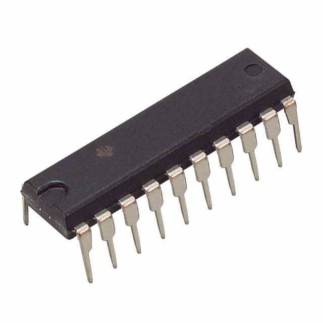


 工商网监
湘ICP备2023018690号
工商网监
湘ICP备2023018690号

