SN74ALS29827, SN74ALS29828
10-BIT BUFFERS AND BUS DRIVERS
WITH 3-STATE OUTPUTS
SDAS095B – JANUARY 1986 – REVISED JANUARY 1995
•
•
•
•
•
•
DW OR NT PACKAGE
(TOP VIEW)
Functionally Equivalent to AMD’s AM29827
and AM29828
3-State Outputs Drive Bus Lines or Buffer
Memory Address Registers
pnp Inputs Reduce dc Loading
Data Flow-Through Pinout (All Inputs on
Opposite Side From Outputs)
Power-Up High-Impedance State
Package Options Include Plastic
Small-Outline (DW) Packages and Standard
Plastic (NT) 300-mil DIPs
OE1
A1
A2
A3
A4
A5
A6
A7
A8
A9
A10
GND
description
These 10-bit buffers and bus drivers provide
high-performance bus interface for wide data
paths or buses carrying parity.
1
24
2
23
3
22
4
21
5
20
6
19
7
18
8
17
9
16
10
15
11
14
12
13
VCC
Y1
Y2
Y3
Y4
Y5
Y6
Y7
Y8
Y9
Y10
OE2
The 3-state control gate is a 2-input NOR such that if either output-enable (OE1 or OE2) input is high, all
ten outputs are in the high-impedance state.
The SN74ALS29827 provides true data and the SN74ALS29828 provides inverted data at their respective
outputs.
The SN74ALS29827 and SN74ALS29828 are characterized for operation from 0°C to 70°C.
logic symbols†
SN74ALS29827
1
OE1
OE2
A1
A2
A3
A4
A5
A6
A7
A8
A9
A10
13
SN74ALS29828
&
1
OE1
EN
OE2
2
23
3
22
4
21
5
20
6
19
7
18
8
17
9
16
10
15
11
14
Y1
A1
Y2
A2
Y3
A3
Y4
A4
Y5
A5
Y6
A6
Y7
A7
Y8
A8
Y9
A9
Y10
A10
13
&
EN
2
23
3
22
4
21
5
20
6
19
7
18
8
17
9
16
10
15
11
14
Y1
Y2
Y3
Y4
Y5
Y6
Y7
Y8
Y9
Y10
† These symbols are in accordance with ANSI/IEEE Std 91-1984 and IEC Publication 617-12.
Copyright 1995, Texas Instruments Incorporated
PRODUCTION DATA information is current as of publication date.
Products conform to specifications per the terms of Texas Instruments
standard warranty. Production processing does not necessarily include
testing of all parameters.
POST OFFICE BOX 655303
• DALLAS, TEXAS 75265
1
�SN74ALS29827, SN74ALS29828
10-BIT BUFFERS AND BUS DRIVERS
WITH 3-STATE OUTPUTS
SDAS095B – JANUARY 1986 – REVISED JANUARY 1995
logic diagrams (positive logic)
SN74ALS29827
OE1
OE2
A1
SN74ALS29828
1
OE1
13
OE2
2
23
Y1
A1
1
13
23
2
To Nine Other Channels
Y1
To Nine Other Channels
absolute maximum ratings over operating free-air temperature range (unless otherwise noted)†
Supply voltage, VCC . . . . . . . . . . . . . . . . . . . . . . . . . . . . . . . . . . . . . . . . . . . . . . . . . . . . . . . . . . . . . . . . . . . . . . . . 7 V
Input voltage, VI . . . . . . . . . . . . . . . . . . . . . . . . . . . . . . . . . . . . . . . . . . . . . . . . . . . . . . . . . . . . . . . . . . . . . . . . . . 5.5 V
Voltage applied to a disabled 3-state output . . . . . . . . . . . . . . . . . . . . . . . . . . . . . . . . . . . . . . . . . . . . . . . . . . 5.5 V
Operating free-air temperature range, TA . . . . . . . . . . . . . . . . . . . . . . . . . . . . . . . . . . . . . . . . . . . . . . 0°C to 70°C
Storage temperature range . . . . . . . . . . . . . . . . . . . . . . . . . . . . . . . . . . . . . . . . . . . . . . . . . . . . . . . – 65°C to 150°C
† Stresses beyond those listed under “absolute maximum ratings” may cause permanent damage to the device. These are stress ratings only, and
functional operation of the device at these or any other conditions beyond those indicated under “recommended operating conditions” is not
implied. Exposure to absolute-maximum-rated conditions for extended periods may affect device reliability.
recommended operating conditions
SN74ALS29827
SN74ALS29828
VCC
VIH
Supply voltage
VIL
IOH
Low-level input voltage
IOL
TA
2
High-level input voltage
UNIT
MIN
NOM
MAX
4.75
5
5.25
2
V
V
0.8
V
High-level output current
– 24
mA
Low-level output current
48
mA
70
°C
Operating free-air temperature
0
POST OFFICE BOX 655303
• DALLAS, TEXAS 75265
�SN74ALS29827, SN74ALS29828
10-BIT BUFFERS AND BUS DRIVERS
WITH 3-STATE OUTPUTS
SDAS095B – JANUARY 1986 – REVISED JANUARY 1995
electrical characteristics over recommended operating free-air temperature range (unless
otherwise noted)
PARAMETER
SN74ALS29827
SN74ALS29828
TEST CONDITIONS
MIN
VIK
VCC = 4.75 V,
VOH
VCC = 4
4.75
75 V
VOL
IOZH
VCC = 4.75 V,
VCC = 5.25 V,
IOZL
II
VCC = 5.25 V,
VCC = 5.25 V,
IIH
IIL
VCC = 5.25 V,
VCC = 5.25 V,
IOS‡
ICC
VCC = 5.25 V,
VCC = 5.25 V
II = – 18 mA
IOH = – 15 mA
TYP†
UNIT
MAX
– 1.2
2.4
IOH = – 24 mA
IOL = 48 mA
V
V
2
0.35
VO = 2.4 V
VO = 0.4 V
0.5
V
20
µA
– 20
µA
VI = 5.5 V
VI = 2.7 V
0.1
mA
20
µA
VI = 0.4 V
VO = 0
– 0.1
mA
– 250
mA
40
mA
– 75
25
† All typical values are at VCC = 5 V, TA = 25°C.
‡ Not more than one output should be shorted at a time, and the duration of the short circuit should not exceed one second.
switching characteristics (see Figure 1)
PARAMETER
FROM
(INPUT)
TO
(OUTPUT)
TEST CONDITIONS
VCC = 4.75 V to 5.25 V
SN74ALS29827 SN74ALS29828
MIN
tPLH
tPHL
A
Y
CL = 300 pF
tPLH
tPHL
A
Y
CL = 50 pF
tPZH
tPZL
OE
Y
CL = 300 pF
tPZH
tPZL
OE
Y
CL = 50 pF
tPHZ
tPLZ
OE
Y
CL = 50 pF
tPHZ
tPLZ
OE
Y
CL = 5 pF
POST OFFICE BOX 655303
• DALLAS, TEXAS 75265
MAX
MIN
UNIT
MAX
15
14
15
14
8
7
8
7.5
20
20
23
23
15
15
15
15
17
17
12
12
9
9
9
9
ns
ns
ns
ns
ns
ns
3
�SN74ALS29827, SN74ALS29828
10-BIT BUFFERS AND BUS DRIVERS
WITH 3-STATE OUTPUTS
SDAS095B – JANUARY 1986 – REVISED JANUARY 1995
PARAMETER MEASUREMENT INFORMATION
Test Point
VCC
SWITCH POSITION TABLE
S1
From Output
Under Test
RL = 180 Ω
All Diodes
1N916 or 1N3064
R1
1 kΩ
CL
(see Note A)
S2
TEST
S1
S2
tPLH
tPHL
tPZH
tPZL
tPHZ
tPLZ
Closed
Closed
Open
Closed
Closed
Closed
Closed
Closed
Closed
Open
Closed
Closed
LOAD CIRCUIT
3V
1.5 V
Timing Input
High-Level
Pulse
3V
1.5 V
0
0
tw
th
tsu
1.5 V
3V
3V
1.5 V
1.5 V
Data Input
0
Low-Level
Pulse
1.5 V
1.5 V
0
VOLTAGE WAVEFORMS
PULSE DURATIONS
VOLTAGE WAVEFORMS
SETUP AND HOLD TIMES
3V
Output
Control
1.5 V
1.5 V
0
tPZL
tPLZ
≈ 4.5 V
3V
Input
1.5 V
1.5 V
0
1.5 V
1.5 V
VOL
tPHZ
VOH
1.5 V
VOH
Waveform 2
(see Note B)
1.5 V
1.5 V
0.5 V
≈ 1.5 V
≈0
VOL
VOLTAGE WAVEFORMS
PROPAGATION DELAY TIMES
0.5 V
tPZH
tPLH
tPHL
≈ 1.5 V
VOL
VOH
In-Phase
Output
1.5 V
tPHL
tPLH
Out-of-Phase
Output
Waveform 1
(see Note B)
VOLTAGE WAVEFORMS
ENABLE AND DISABLE TIMES, 3-STATE OUTPUTS
NOTES: A. CL includes probe and jig capacitance.
B. Waveform 1 is for an output with internal conditions such that the output is low except when disabled by the output control.
Waveform 2 is for an output with internal conditions such that the output is high except when disabled by the output control.
C. All input pulses are supplied by generators having the following characteristics: PRR ≤ 10 MHz, ZO = 50 Ω, tr ≤ 2.5 ns, tf ≤ 2.5 ns.
Figure 1. Load Circuit and Voltage Waveforms
4
POST OFFICE BOX 655303
• DALLAS, TEXAS 75265
�PACKAGE OPTION ADDENDUM
www.ti.com
14-Oct-2022
PACKAGING INFORMATION
Orderable Device
Status
(1)
Package Type Package Pins Package
Drawing
Qty
Eco Plan
(2)
Lead finish/
Ball material
MSL Peak Temp
Op Temp (°C)
Device Marking
(3)
Samples
(4/5)
(6)
SN74ALS29827DW
ACTIVE
SOIC
DW
24
25
RoHS & Green
NIPDAU
Level-1-260C-UNLIM
0 to 70
ALS29827
(1)
The marketing status values are defined as follows:
ACTIVE: Product device recommended for new designs.
LIFEBUY: TI has announced that the device will be discontinued, and a lifetime-buy period is in effect.
NRND: Not recommended for new designs. Device is in production to support existing customers, but TI does not recommend using this part in a new design.
PREVIEW: Device has been announced but is not in production. Samples may or may not be available.
OBSOLETE: TI has discontinued the production of the device.
(2)
RoHS: TI defines "RoHS" to mean semiconductor products that are compliant with the current EU RoHS requirements for all 10 RoHS substances, including the requirement that RoHS substance
do not exceed 0.1% by weight in homogeneous materials. Where designed to be soldered at high temperatures, "RoHS" products are suitable for use in specified lead-free processes. TI may
reference these types of products as "Pb-Free".
RoHS Exempt: TI defines "RoHS Exempt" to mean products that contain lead but are compliant with EU RoHS pursuant to a specific EU RoHS exemption.
Green: TI defines "Green" to mean the content of Chlorine (Cl) and Bromine (Br) based flame retardants meet JS709B low halogen requirements of
很抱歉,暂时无法提供与“SN74ALS29827NT”相匹配的价格&库存,您可以联系我们找货
免费人工找货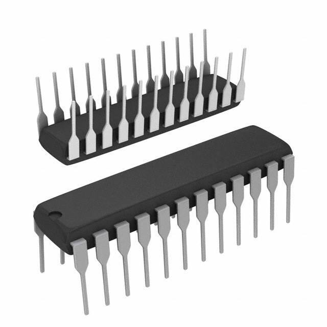


 工商网监
湘ICP备2023018690号
工商网监
湘ICP备2023018690号
