����������� �� �������
���
���� ������� �����������
�����
�
���� �������������
�������
SDAS034C − APRIL 1982 − REVISED FEBRUARY 2009
D Package Options Include Plastic
SN54ALS33A . . . J PACKAGE
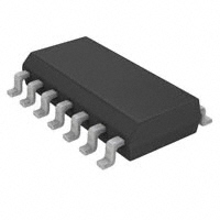
SN74ALS33A . . . D OR N PACKAGE
(TOP VIEW)
Small-Outline (D) Packages, Ceramic Chip
Carriers (FK), and Standard Plastic (N) and
Ceramic (J) 300-mil DIPs
1Y
1A
1B
2Y
2A
2B
GND
description
These devices contain four independent 2-input
positive-NOR buffers with open-collector outputs.
Open-collector outputs require resistive pullup to
perform correctly. They can deliver higher VOH
levels and commonly are used in wired-AND
applications. These devices perform the Boolean
functions Y = A • B or Y = A + B in positive logic.
OUTPUT
Y
H
X
L
X
H
L
L
L
H
1B
2A
2B
3A
3B
4A
4B
2
3
12
4
11
5
10
6
9
7
8
4
3 2 1 20 19
18
5
17
6
16
7
15
8
14
9 10 11 12 13
4B
NC
4A
NC
3Y
NC − No internal connection
logic symbol†
1A
13
3
2B
GND
NC
3A
3B
B
2
VCC
4Y
4B
4A
3Y
3B
3A
1A
1Y
NC
VCC
4Y
1B
NC
2Y
NC
2A
FUNCTION TABLE
(each gate)
A
14
SN54ALS33A . . . FK PACKAGE
(TOP VIEW)
The SN54ALS33A is characterized for operation
over the full military temperature range of − 55°C
to 125°C. The SN74ALS33A is characterized for
operation from 0°C to 70°C.
INPUTS
1
logic diagram (positive logic)
≥1
5
1
4
6
1A
1Y
1B
2A
2Y
2B
8
9
10
3Y
3B
11
12
3A
13
4Y
4A
4B
2
1
3
5
4
6
8
10
9
11
12
13
1Y
2Y
3Y
4Y
† This symbol is in accordance with ANSI/IEEE Std 91-1984 and
IEC Publication 617-12.
Pin numbers shown are for the D, J, and N packages.
Copyright 2009, Texas Instruments Incorporated
�
�������� ���� �����!"#��� �$ %&��'�# "$ �� (&)*�%"#��� +"#',
���+&%#$ %�����! #� $('%���%"#���$ ('� #-' #'�!$ �� �'."$ ��$#�&!'�#$
$#"�+"�+ /"��"�#0, ���+&%#��� (��%'$$��1 +�'$ ��# �'%'$$"��*0 ��%*&+'
#'$#��1 �� "** ("�"!'#'�$,
POST OFFICE BOX 655303
• DALLAS, TEXAS 75265
1
������������ �� �������
���
���� ������� �����������
�����
�
���� �������������
�������
SDAS034C − APRIL 1982 − REVISED FEBRUARY 2009
absolute maximum ratings over operating free-air temperature range (unless otherwise noted)†
Supply voltage, VCC . . . . . . . . . . . . . . . . . . . . . . . . . . . . . . . . . . . . . . . . . . . . . . . . . . . . . . . . . . . . . . . . . . . . . . . . 7 V
Input voltage, VI . . . . . . . . . . . . . . . . . . . . . . . . . . . . . . . . . . . . . . . . . . . . . . . . . . . . . . . . . . . . . . . . . . . . . . . . . . . . 7 V
Off-state output voltage . . . . . . . . . . . . . . . . . . . . . . . . . . . . . . . . . . . . . . . . . . . . . . . . . . . . . . . . . . . . . . . . . . . . . . 7 V
Operating free-air temperature range, TA: SN54ALS33A . . . . . . . . . . . . . . . . . . . . . . . . . . . . . . −55°C to 125°C
SN74ALS33A . . . . . . . . . . . . . . . . . . . . . . . . . . . . . . . . . 0°C to 70°C
Storage temperature range . . . . . . . . . . . . . . . . . . . . . . . . . . . . . . . . . . . . . . . . . . . . . . . . . . . . . . . . −65°C to 150°C
† Stresses beyond those listed under “absolute maximum ratings” may cause permanent damage to the device. These are stress ratings only, and
functional operation of the device at these or any other conditions beyond those indicated under “recommended operating conditions” is not
implied. Exposure to absolute-maximum-rated conditions for extended periods may affect device reliability.
recommended operating conditions
SN54ALS33A
SN74ALS33A
MIN
NOM
MAX
MIN
NOM
MAX
4.5
5
5.5
4.5
5
5.5
UNIT
VCC
VIH
Supply voltage
VIL
VOH
Low-level input voltage
0.7
0.8
V
High-level output voltage
5.5
5.5
V
IOL
TA
Low-level output current
24
mA
70
°C
High-level input voltage
2
2
V
12
Operating free-air temperature
−55
125
V
0
electrical characteristics over recommended operating free-air temperature range (unless
otherwise noted)
PARAMETER
VIK
SN54ALS33A
TYP‡
MAX
TEST CONDITIONS
VCC = 4.5 V,
VOL
VCC = 4.5 V
II
IIH
VCC = 5.5 V,
VCC = 5.5 V,
IIL
IOH
VCC = 5.5 V,
VCC = 4.5 V,
ICCH
ICCL
VCC = 5.5 V,
VCC = 5.5 V,
MIN
II = −18 mA
IOL = 12 mA
SN74ALS33A
TYP‡
MAX
MIN
−1.5
0.25
IOL = 24 mA
VI = 7 V
VI = 2.7 V
VI = 0.4 V
−1.5
0.4
0.25
0.4
0.35
0.5
UNIT
V
V
0.1
0.1
mA
20
20
µA
−0.1
−0.1
mA
0.1
0.1
mA
VOH = 5.5 V
VI = 0
1.7
2.8
1.7
2.8
mA
VI = 4.5 V
5.6
9
5.6
9
mA
‡ All typical values are at VCC = 5 V, TA = 25°C.
switching characteristics (see Figure 1)
PARAMETER
FROM
(INPUT)
TO
(OUTPUT)
VCC = 4.5 V to 5.5 V,
CL = 50 pF,
RL = 680 Ω,
TA = MIN to MAX§
SN54ALS33A
tPLH
tPHL
A or B
Y
MIN
MAX
MIN
MAX
10
59
10
33
2
18
2
12
§ For conditions shown as MIN or MAX, use the appropriate value specified under recommended operating conditions.
2
POST OFFICE BOX 655303
• DALLAS, TEXAS 75265
UNIT
SN74ALS33A
ns
������������ �� �������
���
���� ������� �����������
�����
�
���� �������������
�������
SDAS034C − APRIL 1982 − REVISED FEBRUARY 2009
PARAMETER MEASUREMENT INFORMATION
SERIES 54ALS/74ALS AND 54AS/74AS DEVICES
7V
RL = R1 = R2
VCC
S1
RL
R1
Test
Point
From Output
Under Test
CL
(see Note A)
From Output
Under Test
RL
Test
Point
From Output
Under Test
CL
(see Note A)
CL
(see Note A)
LOAD CIRCUIT FOR
BI-STATE
TOTEM-POLE OUTPUTS
3.5 V
High-Level
Pulse
1.3 V
R2
LOAD CIRCUIT
FOR 3-STATE OUTPUTS
LOAD CIRCUIT
FOR OPEN-COLLECTOR OUTPUTS
3.5 V
Timing
Input
Test
Point
1.3 V
1.3 V
0.3 V
0.3 V
tsu
Data
Input
tw
th
3.5 V
1.3 V
3.5 V
Low-Level
Pulse
1.3 V
0.3 V
1.3 V
0.3 V
VOLTAGE WAVEFORMS
SETUP AND HOLD TIMES
VOLTAGE WAVEFORMS
PULSE DURATIONS
3.5 V
Output
Control
(low-level
enabling)
1.3 V
1.3 V
0.3 V
tPZL
Waveform 1
S1 Closed
(see Note B)
tPLZ
tPHZ
1.3 V
1.3 V
0.3 V
tPHL
[3.5 V
tPLH
VOL
0.3 V
VOH
1.3 V
3.5 V
Input
1.3 V
tPZH
Waveform 2
S1 Open
(see Note B)
1.3 V
0.3 V
[0 V
VOH
In-Phase
Output
1.3 V
1.3 V
VOL
tPLH
tPHL
VOH
Out-of-Phase
Output
(see Note C)
1.3 V
1.3 V
VOL
VOLTAGE WAVEFORMS
PROPAGATION DELAY TIMES
VOLTAGE WAVEFORMS
ENABLE AND DISABLE TIMES, 3-STATE OUTPUTS
NOTES: A. CL includes probe and jig capacitance.
B. Waveform 1 is for an output with internal conditions such that the output is low except when disabled by the output control.
Waveform 2 is for an output with internal conditions such that the output is high except when disabled by the output control.
C. When measuring propagation delay items of 3-state outputs, switch S1 is open.
D. All input pulses have the following characteristics: PRR ≤ 1 MHz, tr = tf = 2 ns, duty cycle = 50%.
E. The outputs are measured one at a time with one transition per measurement.
Figure 1. Load Circuits and Voltage Waveforms
POST OFFICE BOX 655303
• DALLAS, TEXAS 75265
3
�PACKAGE OPTION ADDENDUM
www.ti.com
25-Nov-2021
PACKAGING INFORMATION
Orderable Device
Status
(1)
Package Type Package Pins Package
Drawing
Qty
Eco Plan
(2)
Lead finish/
Ball material
MSL Peak Temp
Op Temp (°C)
(3)
Device Marking
(4/5)
(6)
SN54ALS33AJ
ACTIVE
CDIP
J
14
1
Non-RoHS
& Green
SNPB
N / A for Pkg Type
-55 to 125
SN54ALS33AJ
(1)
The marketing status values are defined as follows:
ACTIVE: Product device recommended for new designs.
LIFEBUY: TI has announced that the device will be discontinued, and a lifetime-buy period is in effect.
NRND: Not recommended for new designs. Device is in production to support existing customers, but TI does not recommend using this part in a new design.
PREVIEW: Device has been announced but is not in production. Samples may or may not be available.
OBSOLETE: TI has discontinued the production of the device.
(2)
RoHS: TI defines "RoHS" to mean semiconductor products that are compliant with the current EU RoHS requirements for all 10 RoHS substances, including the requirement that RoHS substance
do not exceed 0.1% by weight in homogeneous materials. Where designed to be soldered at high temperatures, "RoHS" products are suitable for use in specified lead-free processes. TI may
reference these types of products as "Pb-Free".
RoHS Exempt: TI defines "RoHS Exempt" to mean products that contain lead but are compliant with EU RoHS pursuant to a specific EU RoHS exemption.
Green: TI defines "Green" to mean the content of Chlorine (Cl) and Bromine (Br) based flame retardants meet JS709B low halogen requirements of
很抱歉,暂时无法提供与“SN74ALS33AD”相匹配的价格&库存,您可以联系我们找货
免费人工找货