SN74ALS666, SN74ALS667
8-BIT D-TYPE TRANSPARENT READ-BACK LATCHES
WITH 3-STATE OUTPUTS
SDAS227A – JUNE 1984 – REVISED JANUARY 1995
•
•
•
•
•
3-State I/O-Type Read-Back Inputs
Bus-Structured Pinout
Choice of True or Inverting Logic
– SN74ALS666 . . . True Outputs
– SN74ALS667 . . . Inverted Outputs
Preset and Clear Inputs
Package Options Include Plastic
Small-Outline (DW) Packages and Standard
Plastic (NT) 300-mil DIPs
description
These 8-bit D-type transparent latches are
designed specifically for storing the contents of
the input data bus, plus reading back the stored
data onto the input data bus. In addition, they
provide a 3-state buffer-type output and are easily
utilized in bus-structured applications.
While the latch enable (LE) is high, the Q outputs
of the SN74ALS666 follow the data (D) inputs. The
Q outputs of the SN74ALS667 provide the inverse
of the data applied to its D inputs. The Q or
Q output of both devices is in the high-impedance
state if either output-enable (OE1 or OE2) input is
at a high logic level.
Read back is provided through the read-back
control (OERB) input. When OERB is taken low,
the data present at the output of the data latches
passes back onto the input data bus. When OERB
is taken high, the output of the data latches is
isolated from the D inputs. OERB does not affect
the internal operation of the latches; however,
caution should be exercised to avoid a bus
conflict.
SN74ALS666 . . . DW OR NT PACKAGE
(TOP VIEW)
OERB
OE1
1D
2D
3D
4D
5D
6D
7D
8D
CLR
GND
1
24
2
23
3
22
4
21
5
20
6
19
7
18
8
17
9
16
10
15
11
14
12
13
VCC
OE2
1Q
2Q
3Q
4Q
5Q
6Q
7Q
8Q
PRE
LE
SN74ALS667 . . . DW OR NT PACKAGE
(TOP VIEW)
OERB
OE1
1D
2D
3D
4D
5D
6D
7D
8D
CLR
GND
1
24
2
23
3
22
4
21
5
20
6
19
7
18
8
17
9
16
10
15
11
14
12
13
VCC
OE2
1Q
2Q
3Q
4Q
5Q
6Q
7Q
8Q
PRE
LE
The SN74ALS666 and SN74ALS667 are
characterized for operation from 0°C to 70°C.
Copyright 1995, Texas Instruments Incorporated
PRODUCTION DATA information is current as of publication date.
Products conform to specifications per the terms of Texas Instruments
standard warranty. Production processing does not necessarily include
testing of all parameters.
POST OFFICE BOX 655303
• DALLAS, TEXAS 75265
1
�SN74ALS666, SN74ALS667
8-BIT D-TYPE TRANSPARENT READ-BACK LATCHES
WITH 3-STATE OUTPUTS
SDAS227A – JUNE 1984 – REVISED JANUARY 1995
logic symbols†
SN74ALS666
&
2
OE1
OE2
OERB
14
PRE
11
CLR
LE
1D
13
3
OE2
EN3
2D
3D
4D
5D
6D
7D
8D
OERB
S
1
14
11
CLR
C1
LE
1D
22
2
4
21
5
20
6
19
7
18
8
17
9
16
10
15
1D
13
3
1Q
2Q
3Q
2D
3D
4D
5Q
5D
6Q
6D
7Q
7D
POST OFFICE BOX 655303
S
R
C1
1D
8D
22
2
1Q
4
21
5
20
6
19
7
18
8
17
9
16
10
15
† These symbols are in accordance with ANSI/IEEE Std 91-1984 and IEC Publication 617-12.
2
EN3
3
4Q
8Q
EN2
23
PRE
R
3
&
2
OE1
EN2
23
1
SN74ALS667
• DALLAS, TEXAS 75265
2Q
3Q
4Q
5Q
6Q
7Q
8Q
�SN74ALS666, SN74ALS667
8-BIT D-TYPE TRANSPARENT READ-BACK LATCHES
WITH 3-STATE OUTPUTS
SDAS227A – JUNE 1984 – REVISED JANUARY 1995
logic diagrams (positive logic)
OE1
OE2
OERB
PRE
CLR
LE
1D
2
SN74ALS666
23
1
14
11
13
S
3
1D
22
C1
1Q
R
To Seven Other Channels
OE1
OE2
OERB
PRE
CLR
LE
1D
2
SN74ALS667
23
1
14
11
13
S
3
1D
C1
22
1Q
R
To Seven Other Channels
POST OFFICE BOX 655303
• DALLAS, TEXAS 75265
3
�SN74ALS666, SN74ALS667
8-BIT D-TYPE TRANSPARENT READ-BACK LATCHES
WITH 3-STATE OUTPUTS
SDAS227A – JUNE 1984 – REVISED JANUARY 1995
timing diagram
Data Bus
Input Data
tsu
Input Data
Read Back
th
LE
tsu†
tdis
OERB
tpd
tpd
Q
CLR = H, PRE = H, OE1 = L, OE2 = L.
† This setup time ensures the read-back circuit does not create a conflict on the input data bus.
absolute maximum ratings over operating free-air temperature range (unless otherwise noted)‡
Supply voltage, VCC . . . . . . . . . . . . . . . . . . . . . . . . . . . . . . . . . . . . . . . . . . . . . . . . . . . . . . . . . . . . . . . . . . . . . . . . 7 V
Input voltage, VI (all inputs except D inputs) . . . . . . . . . . . . . . . . . . . . . . . . . . . . . . . . . . . . . . . . . . . . . . . . . . . . 7 V
Voltage applied to D inputs and to disabled 3-state outputs . . . . . . . . . . . . . . . . . . . . . . . . . . . . . . . . . . . . . 5.5 V
Operating free-air temperature range, TA: SN74ALS666, SN74ALS667 . . . . . . . . . . . . . . . . . . . . 0°C to 70°C
Storage temperature range . . . . . . . . . . . . . . . . . . . . . . . . . . . . . . . . . . . . . . . . . . . . . . . . . . . . . . . – 65°C to 150°C
‡ Stresses beyond those listed under “absolute maximum ratings” may cause permanent damage to the device. These are stress ratings only, and
functional operation of the device at these or any other conditions beyond those indicated under “recommended operating conditions” is not
implied. Exposure to absolute-maximum-rated conditions for extended periods may affect device reliability.
recommended operating conditions
SN74ALS666
SN74ALS667
VCC
VIH
Supply voltage
VIL
Low-level input voltage
High-level input voltage
IOH
High level output current
High-level
IOL
Low level output current
Low-level
tw
Pulse duration
NOM
MAX
4.5
5
5.5
2
0.8
– 2.6
D
– 0.4
Q
24
D
8
LE high
10
CLR low
10
PRE low
10
Data before LE↓
10
Data before OERB↓
10
Setup time
th
TA
Hold time, data after LE↓
5
Operating free-air temperature
0
POST OFFICE BOX 655303
• DALLAS, TEXAS 75265
V
V
Q
tsu
4
UNIT
MIN
V
mA
mA
ns
ns
ns
70
°C
�SN74ALS666, SN74ALS667
8-BIT D-TYPE TRANSPARENT READ-BACK LATCHES
WITH 3-STATE OUTPUTS
SDAS227A – JUNE 1984 – REVISED JANUARY 1995
electrical characteristics over recommended operating free-air temperature range (unless
otherwise noted)
PARAMETER
TEST CONDITIONS
SN74ALS666
SN74ALS667
MIN
VIK
VOH
All outputs
VCC = 4.5 V,
VCC = 4.5 V to 5.5 V,
II = – 18 mA
IOH = – 0.4 mA
Q or Q
VCC = 4.5 V,
D inputs
VCC = 4
4.5
5V
IOH = – 2.6 mA
IOL = 4 mA
VOL
IOZH
IOZL
II
IIH
IIL
Q or Q
5V
VCC = 4
4.5
Q or Q
VCC = 5.5 V,
VCC = 5.5 V,
Q or Q
D inputs
All others
D inputs‡
All others
D inputs‡
All others
IO§
SN74ALS666
VCC = 5
5.5
5V
SN74ALS667
VCC – 2
2.4
0.35
0.5
0.25
0.4
IOL = 24 mA
VO = 2.7 V
0.35
0.5
VO = 0.4 V
VI = 5.5 V
VI = 0
0.4
4V
VCC = 5.5 V,
VO = 2.25 V
Q outputs high
20
µA
µA
0.1
20
20
– 0.1
– 0.1
– 30
V
– 20
0.1
VI = 7 V
V
V
3.2
IOL = 8 mA
IOL = 12 mA
VCC = 5
5.5
5V
V,
VCC = 5.5
55V
V,
OERB high
– 1.2
0.4
7V
VI = 2
2.7
ICC
UNIT
MAX
0.25
5V
VCC = 5
5.5
V,
VCC = 5.5
5 5 V,
V
OERB high
TYP†
–112
25
50
Q outputs low
40
73
Q outputs disabled
30
55
Q outputs high
25
50
Q outputs low
45
79
Q outputs disabled
30
mA
µA
mA
mA
mA
60
† All typical values are at VCC = 5 V, TA = 25°C.
‡ For I/O ports (QA through QH), the parameters IIH and IIL include the off-state output current.
§ The output conditions have been chosen to produce a current that closely approximates one half of the true short-circuit output current, IOS.
POST OFFICE BOX 655303
• DALLAS, TEXAS 75265
5
�SN74ALS666, SN74ALS667
8-BIT D-TYPE TRANSPARENT READ-BACK LATCHES
WITH 3-STATE OUTPUTS
SDAS227A – JUNE 1984 – REVISED JANUARY 1995
switching characteristics (see Figure 1)
PARAMETER
FROM
(INPUT)
TO
(OUTPUT)
MAX
3
14
4
18
6
21
8
27
Q
9
29
D
11
32
Q
7
22
D
9
28
OERB
D
4
21
OE1, OE2
Q
4
21
OERB
D
1
14
OE1, OE2
Q
1
14
D
Q
tPLH
tPHL
LE
Q
tPHL
CLR
tPHL
ten‡
tdi
dis§
PRE
UNIT
SN74ALS666
MIN
tPLH
tPHL
tPLH
VCC = 4.5 V to 5.5 V,
CL = 50 pF,
TA = MIN to MAX†
ns
ns
ns
ns
ns
ns
† For conditions shown as MIN or MAX, use the appropriate value specified under recommended operating conditions.
‡ ten = tPZH or tPZL
§ tdis = tPHZ or tPLZ
switching characteristics (see Figure 1)
PARAMETER
FROM
(INPUT)
TO
(OUTPUT)
MAX
6
20
4
15
9
28
7
22
Q
7
24
D
8
26
Q
8
25
D
9
28
D
Q
tPLH
tPHL
LE
Q
tPHL
CLR
tPHL
ten‡
tdi
dis§
PRE
OERB
D
4
21
OE1, OE2
Q
4
21
OERB
D
1
14
Q
1
14
OE1, OE2
† For conditions shown as MIN or MAX, use the appropriate value specified under recommended operating conditions.
‡ ten = tPZH or tPZL
§ tdis = tPHZ or tPLZ
6
POST OFFICE BOX 655303
• DALLAS, TEXAS 75265
UNIT
SN74ALS667
MIN
tPLH
tPHL
tPLH
VCC = 4.5 V to 5.5 V,
CL = 50 pF,
TA = MIN to MAX†
ns
ns
ns
ns
ns
ns
�SN74ALS666, SN74ALS667
8-BIT D-TYPE TRANSPARENT READ-BACK LATCHES
WITH 3-STATE OUTPUTS
SDAS227A – JUNE 1984 – REVISED JANUARY 1995
PARAMETER MEASUREMENT INFORMATION
7V
7V
S1
S1
500 Ω
1 kΩ
Test
Point
From Output
Under Test
CL
(see Note A)
CL
(see Note A)
500 Ω
LOAD CIRCUIT FOR Q OR Q OUTPUTS
1 kΩ
LOAD CIRCUIT FOR D OUTPUTS
3.5 V
Timing
Input
Test
Point
From Output
Under Test
1.3 V
3.5 V
High-Level
Pulse
1.3 V
1.3 V
0.3 V
0.3 V
tw
th
tsu
3.5 V
Data
Input
1.3 V
1.3 V
0.3 V
VOLTAGE WAVEFORMS
SETUP AND HOLD TIMES
1.3 V
0.3 V
3.5 V
Output
Control
(low-level
enabling)
1.3 V
tPHL
tPLH
VOH
1.3 V
1.3 V
tPHL
Out-of-Phase
Output
(see Note D)
Waveform 1
S1 Closed
(see Note B)
VOL
tPLH
VOH
1.3 V
1.3 V
VOL
VOLTAGE WAVEFORMS
PROPAGATION DELAY TIMES
1.3 V
0.3 V
tPZL
1.3 V
tPLZ
0.3 V
In-Phase
Output
1.3 V
VOLTAGE WAVEFORMS
PULSE DURATIONS
3.5 V
1.3 V
Input
3.5 V
Low-Level
Pulse
[3.5 V
1.3 V
tPHZ
tPZH
Waveform 2
S1 Open
(see Note B)
VOL
0.3 V
VOH
1.3 V
0.3 V
[0 V
VOLTAGE WAVEFORMS
ENABLE AND DISABLE TIMES, 3-STATE OUTPUTS
NOTES: A. CL includes probe and jig capacitance.
B. Waveform 1 is for an output with internal conditions such that the output is low except when disabled by the output control.
Waveform 2 is for an output with internal conditions such that the output is high except when disabled by the output control.
C. All input pulses have the following characteristics: PRR ≤ 1 MHz, tr = tf = 2 ns, duty cycle = 50%.
D. When measuring propagation delay times of 3-state outputs, switch S1 is open.
Figure 1. Load Circuits and Voltage Waveforms
POST OFFICE BOX 655303
• DALLAS, TEXAS 75265
7
�PACKAGE OPTION ADDENDUM
www.ti.com
14-Oct-2022
PACKAGING INFORMATION
Orderable Device
Status
(1)
Package Type Package Pins Package
Drawing
Qty
Eco Plan
(2)
Lead finish/
Ball material
MSL Peak Temp
Op Temp (°C)
Device Marking
(3)
Samples
(4/5)
(6)
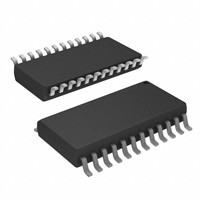
SN74ALS666DW
ACTIVE
SOIC
DW
24
25
RoHS & Green
NIPDAU
Level-1-260C-UNLIM
0 to 70
ALS666
Samples
SN74ALS667DW
ACTIVE
SOIC
DW
24
25
RoHS & Green
NIPDAU
Level-1-260C-UNLIM
0 to 70
ALS667
Samples
(1)
The marketing status values are defined as follows:
ACTIVE: Product device recommended for new designs.
LIFEBUY: TI has announced that the device will be discontinued, and a lifetime-buy period is in effect.
NRND: Not recommended for new designs. Device is in production to support existing customers, but TI does not recommend using this part in a new design.
PREVIEW: Device has been announced but is not in production. Samples may or may not be available.
OBSOLETE: TI has discontinued the production of the device.
(2)
RoHS: TI defines "RoHS" to mean semiconductor products that are compliant with the current EU RoHS requirements for all 10 RoHS substances, including the requirement that RoHS substance
do not exceed 0.1% by weight in homogeneous materials. Where designed to be soldered at high temperatures, "RoHS" products are suitable for use in specified lead-free processes. TI may
reference these types of products as "Pb-Free".
RoHS Exempt: TI defines "RoHS Exempt" to mean products that contain lead but are compliant with EU RoHS pursuant to a specific EU RoHS exemption.
Green: TI defines "Green" to mean the content of Chlorine (Cl) and Bromine (Br) based flame retardants meet JS709B low halogen requirements of


 工商网监
湘ICP备2023018690号
工商网监
湘ICP备2023018690号
