���������
���������� ������������
���������� �
������
���
�������������
����� ��������������
SDAS036D − APRIL 1982 − REVISED AUGUST 1995
•
•
•
SN54ALS873B, SN54AS873A . . . JT PACKAGE
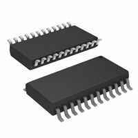
SN74ALS873B, SN74AS873A . . . DW OR NT PACKAGE
(TOP VIEW)
3-State Buffer-Type Outputs Drive Bus
Lines Directly
Bus-Structured Pinout
Package Options Include Plastic
Small-Outline (DW) Packages, Ceramic
Chip Carriers (FK), and Plastic (NT) and
Ceramic (JT) DIPs
1CLR
1OE
1D1
1D2
1D3
1D4
2D1
2D2
2D3
2D4
2OE
GND
description
These dual 4-bit D-type latches feature 3-state
outputs designed specifically for bus driving.
These devices are particularly suitable for
implementing buffer registers, I/O ports,
bidirectional bus drivers, and working registers.
The dual 4-bit latches are transparent D-type
latches. While the latch-enable (LE) input is high,
the Q outputs follow the data (D) inputs in true
form, according to the function table. When LE is
low, the outputs are latched. When the clear (CLR)
input goes low, the Q outputs go low
independently of LE. The outputs are in the
high-impedance state when the output-enable
(OE) input is at a high logic level.
1
24
2
23
3
22
4
21
5
20
6
19
7
18
8
17
9
16
10
15
11
14
12
13
VCC
1LE
1Q1
1Q2
1Q3
1Q4
2Q1
2Q2
2Q3
2Q4
2LE
2CLR
1D1
1OE
1CLR
NC
VCC
1LE
1Q1
SN54ALS873B, SN54AS873A . . . FK PACKAGE
(TOP VIEW)
4
1D2
1D3
1D4
NC
2D1
2D2
2D3
3 2 1 28 27 26
25
6
24
7
23
8
22
9
21
10
20
19
11
12 13 14 15 16 17 18
1Q2
1Q3
1Q4
NC
2Q1
2Q2
2Q3
2D4
2OE
GND
NC
2CLR
2LE
2Q4
The SN54ALS873B and SN54AS873A are
characterized for operation over the full military
temperature range of − 55°C to 125°C. The
SN74ALS873B
and
SN74AS873A
are
characterized for operation from 0°C to 70°C.
5
NC − No internal connection
FUNCTION TABLE
(each latch)
INPUTS
OE
CLR
LE
D
OUTPUT
Q
L
L
X
X
L
L
H
H
H
H
L
H
H
L
L
L
H
L
X
Q0
H
X
X
X
Z
Copyright 1995, Texas Instruments Incorporated
���
������
��� ������!"��� �# $%��&�" !# �� '%()�$!"��� *!"&+
���*%$"# $������ "� #'&$���$!"���# '&� ",& "&��# �� �&-!# ��#"�%�&�"#
#"!�*!�* .!��!�"/+ ���*%$"��� '��$&##��0 *�&# ��" �&$&##!��)/ ��$)%*&
"&#"��0 �� !)) '!�!�&"&�#+
• DALLAS, TEXAS 75265
• HOUSTON, TEXAS 77251−1443
POST OFFICE BOX 655303
POST OFFICE BOX 1443
1
����������
���������� ������������
���������� �
������
���
�������������
����� ��������������
SDAS036D − APRIL 1982 − REVISED AUGUST 1995
logic symbol†
2
1OE
1LE
23
1
1CLR
1D1
1D2
1D3
1D4
3
2LE
2CLR
2D1
2D2
2D3
2D4
OE
EN
C1
C
LE
22
1D
4
21
5
20
6
19
11
2OE
logic diagram (each quad latch, positive logic)
14
13
7
1Q1
CLR
1Q2
R
C1
1Q3
D1
1Q4
Q1
1D
R
C1
EN
D2
C1
Q2
1D
C
18
1D
8
17
9
16
10
15
R
C1
2Q1
D3
2Q2
Q3
1D
2Q3
R
C1
2Q4
D4
Q4
1D
† This symbol is in accordance with ANSI/IEEE Std 91-1984 and
IEC Publication 617-12.
Pin numbers shown are for the DW, JT, and NT packages.
absolute maximum ratings over operating free-air temperature range (unless otherwise noted)‡
Supply voltage, VCC . . . . . . . . . . . . . . . . . . . . . . . . . . . . . . . . . . . . . . . . . . . . . . . . . . . . . . . . . . . . . . . . . . . . . . . . 7 V
Input voltage, VI . . . . . . . . . . . . . . . . . . . . . . . . . . . . . . . . . . . . . . . . . . . . . . . . . . . . . . . . . . . . . . . . . . . . . . . . . . . . 7 V
Voltage applied to a disabled 3-state output . . . . . . . . . . . . . . . . . . . . . . . . . . . . . . . . . . . . . . . . . . . . . . . . . . 5.5 V
Operating free-air temperature range, TA: SN54ALS873B . . . . . . . . . . . . . . . . . . . . . . . . . . . . −55°C to 125°C
SN74ALS873B . . . . . . . . . . . . . . . . . . . . . . . . . . . . . . . 0°C to 70°C
Storage temperature range . . . . . . . . . . . . . . . . . . . . . . . . . . . . . . . . . . . . . . . . . . . . . . . . . . . . . . . . −65°C to 150°C
‡ Stresses beyond those listed under “absolute maximum ratings” may cause permanent damage to the device. These are stress ratings only, and
functional operation of the device at these or any other conditions beyond those indicated under “recommended operating conditions” is not
implied. Exposure to absolute-maximum-rated conditions for extended periods may affect device reliability.
recommended operating conditions
SN54ALS873B
SN74ALS873B
MIN
NOM
MAX
MIN
NOM
MAX
4.5
5
5.5
4.5
5
5.5
UNIT
VCC
VIH
Supply voltage
VIL
IOH
Low-level input voltage
0.7
0.8
V
High-level output current
−1
−2.6
mA
IOL
TA
Low-level output current
24
mA
70
°C
2
High-level input voltage
2
2
12
Operating free-air temperature
−55
•
POST OFFICE BOX 655303 DALLAS, TEXAS 75265
POST OFFICE BOX 1443 HOUSTON, TEXAS 77251−1443
•
125
0
V
V
����������
���������� ������������
���������� �
������
���
�������������
����� ��������������
SDAS036D − APRIL 1982 − REVISED AUGUST 1995
electrical characteristics over recommended operating free-air temperature range (unless
otherwise noted)
PARAMETER
VIK
SN54ALS873B
TYP†
MAX
TEST CONDITIONS
MIN
VCC = 4.5 V,
VCC = 4.5 V to 5.5 V,
II = − 18 mA
IOH = − 0.4 mA
VCC = 4.5 V
IOH = − 1 mA
IOH = − 2.6 mA
VOL
VCC = 4.5 V
IOL = 12 mA
IOL = 24 mA
IOZH
IOZL
VCC = 5.5 V,
VCC = 5.5 V,
VO = 2.7 V
VO = 0.4 V
II
IIH
VCC = 5.5 V,
VCC = 5.5 V,
VI = 7 V
VI = 2.7 V
IIL
IO‡
VCC = 5.5 V,
VCC = 5.5 V,
VI = 0.4 V
VO = 2.25 V
VOH
ICC
VCC = 5.5 V
SN74ALS873B
TYP†
MAX
MIN
−1.2
VCC − 2
2.4
−1.2
UNIT
V
VCC − 2
3.3
V
2.4
0.25
−20
0.4
3.2
0.25
0.4
0.35
0.5
V
20
20
µA
−20
−20
µA
0.1
0.1
mA
20
20
µA
− 0.2
− 0.2
mA
−112
mA
−112
−30
Outputs high
11
21
11
21
Outputs low
16
29
16
29
Outputs disabled
20
31
20
31
mA
† All typical values are at VCC = 5 V, TA = 25°C.
‡ The output conditions have been chosen to produce a current that closely approximates one half of the true short-circuit output current, IOS.
timing requirements over recommended ranges of supply voltage and operating free-air
temperature (unless otherwise noted) (see Figure 1)
SN54ALS873B
MIN
tw
Pulse duration
tsu
Setup time, data before LE↓
th
Hold time, data after LE↓
•
SN74ALS873B
MIN
MAX
UNIT
CLR low
15
15
LE high
10
10
10
10
ns
7
7
ns
POST OFFICE BOX 655303 DALLAS, TEXAS 75265
POST OFFICE BOX 1443 HOUSTON, TEXAS 77251−1443
•
MAX
ns
3
����������
���������� ������������
���������� �
������
���
�������������
����� ��������������
SDAS036D − APRIL 1982 − REVISED AUGUST 1995
switching characteristics (see Figure 1)
PARAMETER
FROM
(INPUT)
TO
(OUTPUT)
tPLH
tPHL
D
Q
tPLH
tPHL
LE
Q
CLR
Q
tPHL
tPZH
tPZL
tPHZ
VCC = 4.5 V to 5.5 V,
CL = 50 pF,
R1 = 500 Ω,
R2 = 500 Ω,
TA = MIN to MAX†
SN54ALS873B SN74ALS873B
OE
MIN
MAX
MIN
MAX
2
23
2
14
2
17
2
14
8
31
8
22
8
26
8
21
6
27
6
20
4
24
4
18
4
23
4
18
2
10
2
15
Q
2
12
Q
OE
tPLZ
2
30
† For conditions shown as MIN or MAX, use the appropriate value specified under recommended operating conditions.
UNIT
ns
ns
ns
ns
ns
absolute maximum ratings over operating free-air temperature range (unless otherwise noted)‡
Supply voltage, VCC . . . . . . . . . . . . . . . . . . . . . . . . . . . . . . . . . . . . . . . . . . . . . . . . . . . . . . . . . . . . . . . . . . . . . . . . 7 V
Input voltage, VI . . . . . . . . . . . . . . . . . . . . . . . . . . . . . . . . . . . . . . . . . . . . . . . . . . . . . . . . . . . . . . . . . . . . . . . . . . . . 7 V
Voltage applied to a disabled 3-state output . . . . . . . . . . . . . . . . . . . . . . . . . . . . . . . . . . . . . . . . . . . . . . . . . . 5.5 V
Operating free-air temperature range, TA: SN54AS873A . . . . . . . . . . . . . . . . . . . . . . . . . . . . . . −55°C to 125°C
SN74AS873A . . . . . . . . . . . . . . . . . . . . . . . . . . . . . . . . . 0°C to 70°C
Storage temperature range . . . . . . . . . . . . . . . . . . . . . . . . . . . . . . . . . . . . . . . . . . . . . . . . . . . . . . . . −65°C to 150°C
‡ Stresses beyond those listed under “absolute maximum ratings” may cause permanent damage to the device. These are stress ratings only, and
functional operation of the device at these or any other conditions beyond those indicated under “recommended operating conditions” is not
implied. Exposure to absolute-maximum-rated conditions for extended periods may affect device reliability.
recommended operating conditions
SN54AS873A
SN74AS873A
MIN
NOM
MAX
MIN
NOM
MAX
4.5
5
5.5
4.5
5
5.5
UNIT
VCC
VIH
Supply voltage
VIL
IOH
Low-level input voltage
0.8
0.8
V
High-level output current
−12
−15
mA
IOL
TA
Low-level output current
32
48
mA
70
°C
4
High-level input voltage
2
Operating free-air temperature
−55
•
POST OFFICE BOX 655303 DALLAS, TEXAS 75265
POST OFFICE BOX 1443 HOUSTON, TEXAS 77251−1443
•
2
125
0
V
V
����������
���������� ������������
���������� �
������
���
�������������
����� ��������������
SDAS036D − APRIL 1982 − REVISED AUGUST 1995
electrical characteristics over recommended operating free-air temperature range (unless
otherwise noted)
PARAMETER
VIK
SN54AS873A
TYP†
MAX
TEST CONDITIONS
MIN
VCC = 4.5 V,
VCC = 4.5 V to 5.5 V,
II = − 18 mA
IOH = − 2 mA
VCC = 4.5 V
IOH = − 12 mA
IOH = − 15 mA
VOL
VCC = 4.5 V
IOL = 32 mA
IOL = 48 mA
IOZH
IOZL
VCC = 5.5 V,
VCC = 5.5 V,
VO = 2.7 V
VO = 0.4 V
II
IIH
VCC = 5.5 V,
VCC = 5.5 V,
VI = 7 V
VI = 2.7 V
IIL
IO‡
VCC = 5.5 V,
VCC = 5.5 V,
VI = 0.4 V
VO = 2.25 V
VOH
ICC
VCC = 5.5 V
SN74AS873A
TYP†
MAX
MIN
−1.2
VCC − 2
2.4
−1.2
UNIT
V
VCC − 2
3.2
V
2.4
0.25
3.3
0.5
0.35
−30
0.5
V
50
50
µA
−50
−50
µA
0.1
0.1
mA
20
20
µA
− 0.5
− 0.5
mA
−112
mA
−112
−30
Outputs high
68
110
68
110
Outputs low
67
109
67
109
Outputs disabled
80
129
80
129
mA
† All typical values are at VCC = 5 V, TA = 25°C.
‡ The output conditions have been chosen to produce a current that closely approximates one half of the true short-circuit output current, IOS.
timing requirements over recommended ranges of supply voltage and operating free-air
temperature (unless otherwise noted) (see Figure 1)
SN54AS873A
MIN
tw*
Pulse duration
tsu*
Setup time, data before LE↓
MAX
SN74AS873A
MIN
CLR low
5
5
LE high
6
5
2
2
MAX
th*
Hold time, data after LE↓
4.5
4.5
* On products compliant to MIL-STD-883, Class B, this parameter is based on characterization data but is not production tested.
•
POST OFFICE BOX 655303 DALLAS, TEXAS 75265
POST OFFICE BOX 1443 HOUSTON, TEXAS 77251−1443
•
UNIT
ns
ns
ns
5
����������
���������� ������������
���������� �
������
���
�������������
����� ��������������
SDAS036D − APRIL 1982 − REVISED AUGUST 1995
switching characteristics (see Figure 1)
PARAMETER
FROM
(INPUT)
TO
(OUTPUT)
tPLH
tPHL
D
Q
tPLH
tPHL
LE
Q
CLR
Q
tPHL
tPZH
tPZL
tPHZ
OE
Q
VCC = 4.5 V to 5.5 V,
CL = 50 pF,
R1 = 500 Ω,
R2 = 500 Ω,
TA = MIN to MAX†
SN54AS873A SN74AS873A
MIN
MAX
MIN
MAX
3
12.5
3
9.5
3
8.5
3
7.5
6
15.5
6
13
4
9
4
7.5
3
10.5
3
9
2
8
2
6.5
4
11
4
10.5
2
7.5
2
7.5
2
8
Q
OE
tPLZ
2
8.5
† For conditions shown as MIN or MAX, use the appropriate value specified under recommended operating conditions.
6
•
POST OFFICE BOX 655303 DALLAS, TEXAS 75265
POST OFFICE BOX 1443 HOUSTON, TEXAS 77251−1443
•
UNIT
ns
ns
ns
ns
ns
����������
���������� ������������
���������� �
������
���
�������������
����� ��������������
SDAS036D − APRIL 1982 − REVISED AUGUST 1995
PARAMETER MEASUREMENT INFORMATION
7V
SWITCH POSITION TABLE
Open
S1
R1 = 500 Ω
From Output
Under Test
CL = 50 pF
(see Note A)
Test Point
R2 = 500 Ω
TEST
S1
tPLH
tPHL
Open
Open
tPZH
tPZL
Open
Closed
tPHZ
tPLZ
Closed
Open
LOAD CIRCUIT FOR 3-STATE OUTPUTS
3.5 V
High-Level
Pulse
1.3 V
1.3 V
0.3 V
tw
3.5 V
Timing
Input
1.3 V
0.3 V
th
tsu
3.5 V
Data
Input
1.3 V
1.3 V
0.3 V
VOLTAGE WAVEFORMS
PULSE DURATION
1.3 V
1.3 V
3.5 V
Low-Level
Pulse
0.3 V
VOLTAGE WAVEFORMS
SETUP AND HOLD TIMES
3.5 V
Output
Control
tPZL
1.3 V
tPLZ
0.3 V
In-Phase
Output
Waveform 1
S1 Closed
(see Note B)
VOH
1.3 V
VOL
1.3 V
Waveform 2
S1 Open
(see Note B)
VOH
1.3 V
1.3 V
tPZH
tPLH
tPHL
Out-of-Phase
Output
3.5 V
tPHL
tPLH
1.3 V
0.3 V
3.5 V
1.3 V
Input
1.3 V
1.3 V
VOL
VOLTAGE WAVEFORMS
PROPAGATION DELAY TIMES
tPHZ
VOL
0.3 V
VOH
1.3 V
0.3 V
0V
VOLTAGE WAVEFORMS
ENABLE AND DISABLE TIMES, 3-STATE OUTPUTS
NOTES: A. CL includes probe and jig capacitance.
B. Waveform 1 is for an output with internal conditions such that the output is low except when disabled by the output control.
Waveform 2 is for an output with internal conditions such that the output is high except when disabled by the output control.
C. All input pulses are supplied by generators having the following characteristics: PRR ≤ 1 MHz, ZO = 50 Ω, tr ≤ 2 ns, tf ≤ 2 ns.
D. The outputs are measured one at a time with one transition per measurement.
Figure 1. Load Circuit and Voltage Waveforms
•
POST OFFICE BOX 655303 DALLAS, TEXAS 75265
POST OFFICE BOX 1443 HOUSTON, TEXAS 77251−1443
•
7
�PACKAGE OPTION ADDENDUM
www.ti.com
10-Jun-2022
PACKAGING INFORMATION
Orderable Device
Status
(1)
Package Type Package Pins Package
Drawing
Qty
Eco Plan
(2)
Lead finish/
Ball material
MSL Peak Temp
Op Temp (°C)
Device Marking
(3)
Samples
(4/5)
(6)
84032013A
ACTIVE
LCCC
FK
28
1
Non-RoHS
& Green
SNPB
N / A for Pkg Type
-55 to 125
84032013A
SNJ54ALS
873BFK
8403201LA
ACTIVE
CDIP
JT
24
1
Non-RoHS
& Green
SNPB
N / A for Pkg Type
-55 to 125
8403201LA
SNJ54ALS873BJT
Samples
SN74ALS873BDW
ACTIVE
SOIC
DW
24
25
RoHS & Green
NIPDAU
Level-1-260C-UNLIM
0 to 70
ALS873B
Samples
SN74ALS873BDWR
ACTIVE
SOIC
DW
24
2000
RoHS & Green
NIPDAU
Level-1-260C-UNLIM
0 to 70
ALS873B
Samples
SNJ54ALS873BFK
ACTIVE
LCCC
FK
28
1
Non-RoHS
& Green
SNPB
N / A for Pkg Type
-55 to 125
84032013A
SNJ54ALS
873BFK
SNJ54ALS873BJT
ACTIVE
CDIP
JT
24
1
Non-RoHS
& Green
SNPB
N / A for Pkg Type
-55 to 125
8403201LA
SNJ54ALS873BJT
(1)
The marketing status values are defined as follows:
ACTIVE: Product device recommended for new designs.
LIFEBUY: TI has announced that the device will be discontinued, and a lifetime-buy period is in effect.
NRND: Not recommended for new designs. Device is in production to support existing customers, but TI does not recommend using this part in a new design.
PREVIEW: Device has been announced but is not in production. Samples may or may not be available.
OBSOLETE: TI has discontinued the production of the device.
(2)
RoHS: TI defines "RoHS" to mean semiconductor products that are compliant with the current EU RoHS requirements for all 10 RoHS substances, including the requirement that RoHS substance
do not exceed 0.1% by weight in homogeneous materials. Where designed to be soldered at high temperatures, "RoHS" products are suitable for use in specified lead-free processes. TI may
reference these types of products as "Pb-Free".
RoHS Exempt: TI defines "RoHS Exempt" to mean products that contain lead but are compliant with EU RoHS pursuant to a specific EU RoHS exemption.
Green: TI defines "Green" to mean the content of Chlorine (Cl) and Bromine (Br) based flame retardants meet JS709B low halogen requirements of


 工商网监
湘ICP备2023018690号
工商网监
湘ICP备2023018690号
